EP0226207A2 - Elément photosensible pour l'électrophotographie - Google Patents
Elément photosensible pour l'électrophotographie Download PDFInfo
- Publication number
- EP0226207A2 EP0226207A2 EP86117502A EP86117502A EP0226207A2 EP 0226207 A2 EP0226207 A2 EP 0226207A2 EP 86117502 A EP86117502 A EP 86117502A EP 86117502 A EP86117502 A EP 86117502A EP 0226207 A2 EP0226207 A2 EP 0226207A2
- Authority
- EP
- European Patent Office
- Prior art keywords
- layer
- amorphous silicon
- photosensitive member
- member according
- thickness
- Prior art date
- Legal status (The legal status is an assumption and is not a legal conclusion. Google has not performed a legal analysis and makes no representation as to the accuracy of the status listed.)
- Granted
Links
Images


Classifications
-
- G—PHYSICS
- G03—PHOTOGRAPHY; CINEMATOGRAPHY; ANALOGOUS TECHNIQUES USING WAVES OTHER THAN OPTICAL WAVES; ELECTROGRAPHY; HOLOGRAPHY
- G03G—ELECTROGRAPHY; ELECTROPHOTOGRAPHY; MAGNETOGRAPHY
- G03G5/00—Recording-members for original recording by exposure, e.g. to light, to heat or to electrons; Manufacture thereof; Selection of materials therefor
- G03G5/02—Charge-receiving layers
- G03G5/04—Photoconductive layers; Charge-generation layers or charge-transporting layers; Additives therefor; Binders therefor
- G03G5/08—Photoconductive layers; Charge-generation layers or charge-transporting layers; Additives therefor; Binders therefor characterised by the photoconductive material being inorganic
- G03G5/082—Photoconductive layers; Charge-generation layers or charge-transporting layers; Additives therefor; Binders therefor characterised by the photoconductive material being inorganic and not being incorporated in a bonding material, e.g. vacuum deposited
- G03G5/08214—Silicon-based
- G03G5/08221—Silicon-based comprising one or two silicon based layers
Definitions
- This invention relates to a photoconductive member for use in electrophotography, and more particularly to a novel construction of the photoconductive member for use in electrophotography capable of preventing flow and blur of images.
- photoconductive material such as Se, Cds and ZnO
- organic photoconductive material such as poli-n-vynil carbozol and trinitrofluorenone
- amorphous silicon photosensitive member using hydrogenated amorphous silicon layer as a photoconductor have become noted for use in electrophotography because of their excellent heat resistance property, wear resistant property, harmless property and high photosensitivity.
- a photoconductor for use in electrophotography, a photoconductor comprising an aluminum supporting member and an amorphous silicon layer formed thereon to act as a photoconductive layer has been widely used.
- the adhesive force of the amorphous silicon to aluminum is not sufficiently large, we have succeeded to improve the adhesive property by subjecting the surface of an aluminum layer 11 to an almite treatment (oxidation treatment) to form a porous layer 12B formed of an anhydrous amorphous aluminum layer whose surface containing numerous fine pores and then applying a hydrogenated amorphous layer 13 to the porous layer 12b without sealing the fine pores as shown in Fig. 6.
- amorphous boron layer 14 (a-BN) is applied to the upper surface of the hydrogenated amorphous silicon layer.
- the amorphous boron nitride layer 14 has properties of an excellent insulating strength and a small light absorption, and can prevent light reflection and is not influenced by environment condition variation.
- the recording of images is made in the following manner. More particularly, after applying uniform electric charge onto the surface of a photoconductor by using corona discharge, a light image is projected. Due to the absorption of the projected light, electron-hole pairs are formed in the photoconductive layer and the electrons and holes thus formed are caused to migrate due to the surface charge so as to cause to remain the surface charge only at regions not irradiated or exposed to light (formation of a latent image).
- an oppositely charged toner is sprinkled onto the latent image thus formed, the remaining surface charge attracts the toner through the photoconductor layer and the insulative amorphous boron nitride layer, thus developing or visualizing the latent image. Then the developed toner image is transfer printed onto a copying paper. At this time, there is a tendency of flow or blur of the image, thus failing to obtain a clear copy.
- a photosensitive member for use in electrophotography of the type wherein the surface of a supporting member is coated with a porous amorphous aluminum oxide anhydride, a hydrogenated amorphous silicon layer acting as a photoconductive layer, and a hydrogen containing amorphous boron nitride layer acting as a surface layer, characterized by an intermediate layer interposed between the photoconductive layer and the surface layer, the intermediate layer consisting of amorphous silicon nitride (a-SiN) or amorphous silicon carbide (a-SiC).
- a-SiN amorphous silicon nitride
- a-SiC amorphous silicon carbide
- the photosensitive member of this invention for use in electrophotography comprises a lamination of a cylindrical or sheet shaped aluminum 1 having a purity of higher than 99.5% and is formed on its surface with an almite layer not containing any chemically combined water, a hydrolized amorphous silicon layer 3 (a-Si :H) having a thickness of 20 microns, containing hydrogen in 9.3 at.% and formed on the surface of the almite layer to act as a photoconductive layer, and an amorphous silicon nitride layer (a-SiN), having a thickness of 100A and acting as an intermediate layer and a hydrogen containing amorphous boron nitride layer 5 (a-BN) acting as a surface layer.
- a-Si :H hydrolized amorphous silicon layer 3
- a-SiN amorphous silicon nitride layer
- the almite layer is of the double layer construction consisting of a dense barrier layer made of aluminum oxide of a thickness of 100A and a porous layer having a thickness of 1 micron and made of anhydride amorphous aluminum oxide containing numerous micropores.
- an electrolytic treatment is performed using as an anode pure aluminum formed into a cylinder, a sheet or other suitable configuration and electrolyte such as sulfuric acid and oxalic acid so as to form an almite layer 2 consisting of a barrier layer 2a having a thickness of 100A and a porous layer 2b having a thickness of 1 micron.
- the electrolysis voltage was 10 -20V
- the temperature of the electrolyte was 10 -25°C
- the concentration was 10 -20%
- the current density was 1 -2 A /dm2.
- a boron doped hydrogenated amorphous silicon layer 3 having a thickness of 20 micron and containing hydrogen in an amount of 9.3 at % is coated on the surface of the porous layer 2 by plasma CVD method, thereby forming a photoconductive layer.
- the layer forming conditions were as follows: substrate (supporting member) temperature: 325°C; reaction gas: a mixture of silan (SiH,) and diboran (B 2 H 6 ); gas pressure: 1.0 Torr; quantity of gas flow: SiH, 100 SCCM, B 2 H 6 50 SCCM; applied frequency: 13.56 MHz; and power: 100W.
- the hydrogen content of a layer thus formed varies depending upon the substrate temperature. the relation between the substrate temperature and the hydrogen content is shown in Fig. 3.
- an amorphous silicon nitride layer 4 having a thickness of 100A and acting as an intermediate layer 4 is coated on the layer 3 by plasma CVD method.
- the layer forming conditions were: substrate temperature: 325°C; reaction gas: a mixture of silan (SiH,) and ammonium (NH j ); gas pressure 1.0 Torr; quantity of gas flow: SiH, 50 SCCM, NH, 50 SCCM; applied frequency: 13.56 MHz; and power: 100W - (Fig. 2c).
- a hydrogen containing amorphous boron nitride layer having a thickness of 1500A and acting as a surface layer was coated with (CVD method).
- the layer forming conditions were: substrate temperature: 325°C, reaction gas: a mixture of diborane (B 2 H 6 ) and ammonium (NH,); gas pressure: 1.0 Torr; quantity of gas flow B 2 H 6 100 SCCM, NH, 50 SCCM; applied frequency: 13.56 MH 3 , and power: 100W.
- the hydrogenated amorphous silicon layer 3, the amorphous silicon nitride layer 4, and the amorphous boron nitride layer 5 can be consecutively formed by switching the reaction gases.
- the supporting member When forming a layer, the supporting member is set in the reaction chamber of a plasma CVD apparatus and then the reaction chamber is evacuated to a vacuum of about 10- 6 Torr.
- the gas mixture is admitted into the reaction chamber while adjusting the flow quantity with a mass flow controller and then the pressure in the reaction chamber is set to 1.0 Torr with a gas pressure controller.
- the supporting member is grounded and a layer is formed by applying a high frequency power while matching the impedance with an impedance box.
- amorphous boron nitride layer and the amorphous silicon nitride layer are respectively used as the surface layer and the intermediate layer the surface
- the comparison data of the potential, photosensitivity, and the picture image characteristics are shown in Fig. 5 where only the amorphous silicon nitride layer is used as the surface layer and where only the amorphous boron nitride layer is used as the surface layer.
- the surface potential, photosensitivity and picture image characteristics are excellent where amorphous silicon nitride is used as the intermediate layer, and amorphous boron nitride is used as the intermediate layer.
- the quantity of nitrogen content should be less than 40 at %.
- the photosensitive member prepared in the manner described above can prevent flow and blur of the image by the use of an intermediate layer, thereby providing a clear copy.
- the photoconductive layer and the supporting member can be strongly bonded together, and the photoelectric property is excellent.
- the thickness of the barrier layer 2a and the porous layer 2b of the almite layer can be varied by varying the reaction conditions at the anode oxidation step, the relation between the adhesive power and the photoelectric characteristic of the thickness a of the barrier layer 2a, and the thickness of the porous layer 2b (photoconductive layer) is shown in Table III, in which symbol “o” means excellent, “x” inferior and “ ⁇ practically employable although not so excellent.
- This table shows that the adhesive force is increased as the thickness of the porous layer increases and that it is advantageous to limit the thickness of the porous layer to at most 5 microns when one considered the photoelectric characteristic. Although a thin barrier layer is preferred, the photoelectric characteristic will not be affected so long as the thickness lies in a range of 10A -500A.
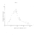
- a photosensitive member was prepared by varying the quantity of hydrogen (at %) in the hydrogenated amorphous silicon layer by changing the composition of the reaction gas, and the relation between the quantity of hydrogen and the charging performance (V/u) was measured.
- the result of measurement is shown in Fig. 4 in which the ordinate shows the charging characteristic and the abscissa shows the hydrogen quantity.
- Fig. 4 clearly shows that especially excellent results can be obtained when the hydrogen content is maintained to be less than 20 at %, especially in a range of 5 -13 at %.
- a photosensitive member comprising a pure aluminum cylinder or sheet formed on its surface with an almite layer not comprising crystalline water, a hydrolized amorphous silicon layer acting as a photoconductive layer, an amorphous silicon nitride layer acting as an intermediate layer and an amorphous boron nitride layer acting as a surface layer, which are laminated sequentially, is free from flow of the image and has excellent properties in the adhesive force and the photoelectric characteristics.
- an amorphous silicon nitride layer was used as the intermediate layer, this layer can be substituted by an amorphous silicon carbide layer.
- the thickness a of the barrier layer of the almite layer on the surface of the supporting member was made to be 100A, and the thickness ⁇ of the porous layer was made to be 6 micron.
- the barrier layer may be omitted. When it is made as thinner as possible, the photoelectric electric characteristic can be improved.
- the barrier layer is inevitably formed at the time of the almite forming treatment so that it is preferable to select the treatment conditions so as to determine a and in the ranges of 10A ⁇ ⁇ ⁇ 500A and 0 ⁇ ⁇ ⁇ 5 ⁇ m.
- the hydrogen content C H of the photoconductive layer is selected to be C H 20 at %, more preferably 5 at % ⁇ C H ⁇ 13 at %, still more preferably 7 at % ⁇ C H ⁇ 10 at %.
- the thickness of the photoconductive layer is selected in a range of 5 ⁇ ⁇ t ⁇ 80u. With less than 5 microns, a desired surface level could not be obtained whereas with higher than 80 microns the photoelectric characteristic would decrease.
- the quantity of boron doped in the photoconductive layer is selected in a range of 10- 7 at % -10- 5 at %. Because with higher than 10- 5 at % of boron, a desired surface potential can not be obtained and since the amorphous silicon is a n type semiconductor in a not doped state, with less than 10- 7 at %, the resistance becomes low, thus failing to obtain a desired surface potential.
- the composition ratio of boron and nitrogen in the amorphous boron nitride comprising the surface layer is selected to be in a range of 0.2 ⁇ x 5 0.8.
- the layer thickness d it is desirable to select it in a range of 0.01 ⁇ ⁇ d 10 ⁇ , preferably 0.05 ⁇ ⁇ d 5 5 ⁇ . If the surface layer were too thin, blocking affect could not be expected whereas if it were too thick the photoelectric effect would degrade.
Landscapes
- Chemical & Material Sciences (AREA)
- Inorganic Chemistry (AREA)
- Physics & Mathematics (AREA)
- General Physics & Mathematics (AREA)
- Photoreceptors In Electrophotography (AREA)
Applications Claiming Priority (2)
| Application Number | Priority Date | Filing Date | Title |
|---|---|---|---|
| JP287437/85 | 1985-12-20 | ||
| JP60287437A JPH083645B2 (ja) | 1985-12-20 | 1985-12-20 | 電子写真感光体 |
Publications (3)
| Publication Number | Publication Date |
|---|---|
| EP0226207A2 true EP0226207A2 (fr) | 1987-06-24 |
| EP0226207A3 EP0226207A3 (en) | 1988-06-01 |
| EP0226207B1 EP0226207B1 (fr) | 1991-03-27 |
Family
ID=17717304
Family Applications (1)
| Application Number | Title | Priority Date | Filing Date |
|---|---|---|---|
| EP86117502A Expired - Lifetime EP0226207B1 (fr) | 1985-12-20 | 1986-12-16 | Elément photosensible pour l'électrophotographie |
Country Status (5)
| Country | Link |
|---|---|
| US (1) | US4699861A (fr) |
| EP (1) | EP0226207B1 (fr) |
| JP (1) | JPH083645B2 (fr) |
| KR (1) | KR940004212B1 (fr) |
| DE (1) | DE3678403D1 (fr) |
Cited By (1)
| Publication number | Priority date | Publication date | Assignee | Title |
|---|---|---|---|---|
| EP0328097A3 (fr) * | 1988-02-10 | 1990-08-22 | Fuji Xerox Co., Ltd. | Procédé de fabrication d'un photorécepteur électrophotographique |
Families Citing this family (4)
| Publication number | Priority date | Publication date | Assignee | Title |
|---|---|---|---|---|
| US4845001A (en) * | 1986-04-30 | 1989-07-04 | Canon Kabushiki Kaisha | Light receiving member for use in electrophotography with a surface layer comprising non-single-crystal material containing tetrahedrally bonded boron nitride |
| US20030180445A1 (en) * | 2002-03-21 | 2003-09-25 | Industrial Scientific Corporation | Method for forming a catalytic bead sensor |
| KR100448714B1 (ko) * | 2002-04-24 | 2004-09-13 | 삼성전자주식회사 | 다층 나노라미네이트 구조를 갖는 반도체 장치의 절연막및 그의 형성방법 |
| DE10327315B4 (de) * | 2003-06-16 | 2007-08-16 | Eastman Kodak Co. | Verfahren zur Aufbereitung eines Trägers für einen Fotoleiter zur Ausbildung eines elektrofotografischen Aufzeichnungselementes und demgemäß ausgebildetes Aufzeichungselement |
Family Cites Families (4)
| Publication number | Priority date | Publication date | Assignee | Title |
|---|---|---|---|---|
| US4464451A (en) * | 1981-02-06 | 1984-08-07 | Canon Kabushiki Kaisha | Electrophotographic image-forming member having aluminum oxide layer on a substrate |
| JPS59128281A (ja) * | 1982-12-29 | 1984-07-24 | 信越化学工業株式会社 | 炭化けい素被覆物の製造方法 |
| JPS6083957A (ja) * | 1983-10-13 | 1985-05-13 | Sharp Corp | 電子写真感光体 |
| US4544617A (en) * | 1983-11-02 | 1985-10-01 | Xerox Corporation | Electrophotographic devices containing overcoated amorphous silicon compositions |
-
1985
- 1985-12-20 JP JP60287437A patent/JPH083645B2/ja not_active Expired - Lifetime
-
1986
- 1986-12-16 EP EP86117502A patent/EP0226207B1/fr not_active Expired - Lifetime
- 1986-12-16 DE DE8686117502T patent/DE3678403D1/de not_active Expired - Lifetime
- 1986-12-16 US US06/942,350 patent/US4699861A/en not_active Expired - Fee Related
- 1986-12-18 KR KR1019860010898A patent/KR940004212B1/ko not_active Expired - Fee Related
Cited By (1)
| Publication number | Priority date | Publication date | Assignee | Title |
|---|---|---|---|---|
| EP0328097A3 (fr) * | 1988-02-10 | 1990-08-22 | Fuji Xerox Co., Ltd. | Procédé de fabrication d'un photorécepteur électrophotographique |
Also Published As
| Publication number | Publication date |
|---|---|
| KR940004212B1 (ko) | 1994-05-17 |
| EP0226207A3 (en) | 1988-06-01 |
| KR870006436A (ko) | 1987-07-11 |
| JPS62147464A (ja) | 1987-07-01 |
| US4699861A (en) | 1987-10-13 |
| JPH083645B2 (ja) | 1996-01-17 |
| DE3678403D1 (de) | 1991-05-02 |
| EP0226207B1 (fr) | 1991-03-27 |
Similar Documents
| Publication | Publication Date | Title |
|---|---|---|
| CA1181628A (fr) | Constituant photoconducteur renfermant une couche non photoconductrice a base d'une matrice de silicium amorphe avec de l'azote | |
| US4600670A (en) | Printing member for electrostatic photocopying | |
| US5976745A (en) | Photosensitive member for electrophotography and fabrication process thereof | |
| US4699861A (en) | Photosensitive member for use in electrophotography | |
| US4853309A (en) | Photoreceptor for electrophotography with a-Si layers having a gradient concentration of doped atoms and sandwiching the photoconductive layer therebetween | |
| US5303007A (en) | Printing apparatus for electrostatic photocopying | |
| US4833055A (en) | Electrophotographic photoreceptor comprising amorphous silicon and amorphous carbon buffer layer | |
| EP0174241B1 (fr) | Méthode de production des éléments photoconductifs isolants avec une bande d'exposition dynamique large | |
| US4804608A (en) | Amorphous silicon photoreceptor for electrophotography | |
| KR910006737B1 (ko) | 전자사진 광수용기 제조방법 | |
| US4619877A (en) | Low field electrophotographic process | |
| US5103262A (en) | Printing member for electrostatic photocopying | |
| JPS6335026B2 (fr) | ||
| JPH0220095B2 (fr) | ||
| Taniguchi et al. | A highly sensitive chalcogenide photoconductor in a near‐infrared wavelength region | |
| JPH0740138B2 (ja) | 電子写真感光体 | |
| Nakayama et al. | Stability of amorphous silicon photoreceptor for diode laser printer application | |
| CA1249476A (fr) | Procede electrophotographique a champ faible | |
| JP2657491B2 (ja) | 電子写真感光体 | |
| JPS6261056A (ja) | 光導電体 | |
| JPH0212159A (ja) | 電子写真用感光体 | |
| JPS60115941A (ja) | 電子写真感光体 | |
| JPS6250766A (ja) | 電子写真感光体 | |
| JP2001343770A (ja) | 感光体および画像形成装置 | |
| JPH0715584B2 (ja) | 電子写真感光体 |
Legal Events
| Date | Code | Title | Description |
|---|---|---|---|
| PUAI | Public reference made under article 153(3) epc to a published international application that has entered the european phase |
Free format text: ORIGINAL CODE: 0009012 |
|
| AK | Designated contracting states |
Kind code of ref document: A2 Designated state(s): DE FR GB |
|
| PUAL | Search report despatched |
Free format text: ORIGINAL CODE: 0009013 |
|
| AK | Designated contracting states |
Kind code of ref document: A3 Designated state(s): DE FR GB |
|
| 17P | Request for examination filed |
Effective date: 19881128 |
|
| 17Q | First examination report despatched |
Effective date: 19900427 |
|
| GRAA | (expected) grant |
Free format text: ORIGINAL CODE: 0009210 |
|
| AK | Designated contracting states |
Kind code of ref document: B1 Designated state(s): DE FR GB |
|
| REF | Corresponds to: |
Ref document number: 3678403 Country of ref document: DE Date of ref document: 19910502 |
|
| ET | Fr: translation filed | ||
| PLBE | No opposition filed within time limit |
Free format text: ORIGINAL CODE: 0009261 |
|
| STAA | Information on the status of an ep patent application or granted ep patent |
Free format text: STATUS: NO OPPOSITION FILED WITHIN TIME LIMIT |
|
| 26N | No opposition filed | ||
| PGFP | Annual fee paid to national office [announced via postgrant information from national office to epo] |
Ref country code: GB Payment date: 19931207 Year of fee payment: 8 |
|
| PGFP | Annual fee paid to national office [announced via postgrant information from national office to epo] |
Ref country code: FR Payment date: 19931209 Year of fee payment: 8 |
|
| PGFP | Annual fee paid to national office [announced via postgrant information from national office to epo] |
Ref country code: DE Payment date: 19941208 Year of fee payment: 9 |
|
| PG25 | Lapsed in a contracting state [announced via postgrant information from national office to epo] |
Ref country code: GB Effective date: 19941216 |
|
| GBPC | Gb: european patent ceased through non-payment of renewal fee |
Effective date: 19941216 |
|
| PG25 | Lapsed in a contracting state [announced via postgrant information from national office to epo] |
Ref country code: FR Effective date: 19950831 |
|
| REG | Reference to a national code |
Ref country code: FR Ref legal event code: ST |
|
| PG25 | Lapsed in a contracting state [announced via postgrant information from national office to epo] |
Ref country code: DE Effective date: 19960903 |