EP0228212A2 - Dispositif à circuit intégré - Google Patents
Dispositif à circuit intégré Download PDFInfo
- Publication number
- EP0228212A2 EP0228212A2 EP86309619A EP86309619A EP0228212A2 EP 0228212 A2 EP0228212 A2 EP 0228212A2 EP 86309619 A EP86309619 A EP 86309619A EP 86309619 A EP86309619 A EP 86309619A EP 0228212 A2 EP0228212 A2 EP 0228212A2
- Authority
- EP
- European Patent Office
- Prior art keywords
- power source
- source substrate
- layers
- integrated circuit
- heat radiating
- Prior art date
- Legal status (The legal status is an assumption and is not a legal conclusion. Google has not performed a legal analysis and makes no representation as to the accuracy of the status listed.)
- Granted
Links
Images


Classifications
-
- H—ELECTRICITY
- H05—ELECTRIC TECHNIQUES NOT OTHERWISE PROVIDED FOR
- H05K—PRINTED CIRCUITS; CASINGS OR CONSTRUCTIONAL DETAILS OF ELECTRIC APPARATUS; MANUFACTURE OF ASSEMBLAGES OF ELECTRICAL COMPONENTS
- H05K1/00—Printed circuits
- H05K1/02—Details
- H05K1/03—Use of materials for the substrate
- H05K1/0313—Organic insulating material
- H05K1/0353—Organic insulating material consisting of two or more materials, e.g. two or more polymers, polymer + filler, + reinforcement
- H05K1/0373—Organic insulating material consisting of two or more materials, e.g. two or more polymers, polymer + filler, + reinforcement containing additives, e.g. fillers
-
- H—ELECTRICITY
- H05—ELECTRIC TECHNIQUES NOT OTHERWISE PROVIDED FOR
- H05K—PRINTED CIRCUITS; CASINGS OR CONSTRUCTIONAL DETAILS OF ELECTRIC APPARATUS; MANUFACTURE OF ASSEMBLAGES OF ELECTRICAL COMPONENTS
- H05K1/00—Printed circuits
- H05K1/02—Details
- H05K1/0272—Adaptations for fluid transport, e.g. channels, holes
-
- H—ELECTRICITY
- H10—SEMICONDUCTOR DEVICES; ELECTRIC SOLID-STATE DEVICES NOT OTHERWISE PROVIDED FOR
- H10W—GENERIC PACKAGES, INTERCONNECTIONS, CONNECTORS OR OTHER CONSTRUCTIONAL DETAILS OF DEVICES COVERED BY CLASS H10
- H10W40/00—Arrangements for thermal protection or thermal control
- H10W40/40—Arrangements for thermal protection or thermal control involving heat exchange by flowing fluids
- H10W40/47—Arrangements for thermal protection or thermal control involving heat exchange by flowing fluids by flowing liquids, e.g. forced water cooling
-
- H—ELECTRICITY
- H10—SEMICONDUCTOR DEVICES; ELECTRIC SOLID-STATE DEVICES NOT OTHERWISE PROVIDED FOR
- H10W—GENERIC PACKAGES, INTERCONNECTIONS, CONNECTORS OR OTHER CONSTRUCTIONAL DETAILS OF DEVICES COVERED BY CLASS H10
- H10W70/00—Package substrates; Interposers; Redistribution layers [RDL]
- H10W70/60—Insulating or insulated package substrates; Interposers; Redistribution layers
- H10W70/611—Insulating or insulated package substrates; Interposers; Redistribution layers for connecting multiple chips together
-
- H—ELECTRICITY
- H10—SEMICONDUCTOR DEVICES; ELECTRIC SOLID-STATE DEVICES NOT OTHERWISE PROVIDED FOR
- H10W—GENERIC PACKAGES, INTERCONNECTIONS, CONNECTORS OR OTHER CONSTRUCTIONAL DETAILS OF DEVICES COVERED BY CLASS H10
- H10W70/00—Package substrates; Interposers; Redistribution layers [RDL]
- H10W70/60—Insulating or insulated package substrates; Interposers; Redistribution layers
- H10W70/67—Insulating or insulated package substrates; Interposers; Redistribution layers characterised by their insulating layers or insulating parts
- H10W70/68—Shapes or dispositions thereof
- H10W70/685—Shapes or dispositions thereof comprising multiple insulating layers
-
- H—ELECTRICITY
- H10—SEMICONDUCTOR DEVICES; ELECTRIC SOLID-STATE DEVICES NOT OTHERWISE PROVIDED FOR
- H10W—GENERIC PACKAGES, INTERCONNECTIONS, CONNECTORS OR OTHER CONSTRUCTIONAL DETAILS OF DEVICES COVERED BY CLASS H10
- H10W90/00—Package configurations
- H10W90/401—Package configurations characterised by multiple insulating or insulated package substrates, interposers or RDLs
-
- H—ELECTRICITY
- H05—ELECTRIC TECHNIQUES NOT OTHERWISE PROVIDED FOR
- H05K—PRINTED CIRCUITS; CASINGS OR CONSTRUCTIONAL DETAILS OF ELECTRIC APPARATUS; MANUFACTURE OF ASSEMBLAGES OF ELECTRICAL COMPONENTS
- H05K2201/00—Indexing scheme relating to printed circuits covered by H05K1/00
- H05K2201/02—Fillers; Particles; Fibers; Reinforcement materials
- H05K2201/0203—Fillers and particles
- H05K2201/0206—Materials
- H05K2201/0209—Inorganic, non-metallic particles
-
- H—ELECTRICITY
- H05—ELECTRIC TECHNIQUES NOT OTHERWISE PROVIDED FOR
- H05K—PRINTED CIRCUITS; CASINGS OR CONSTRUCTIONAL DETAILS OF ELECTRIC APPARATUS; MANUFACTURE OF ASSEMBLAGES OF ELECTRICAL COMPONENTS
- H05K2201/00—Indexing scheme relating to printed circuits covered by H05K1/00
- H05K2201/02—Fillers; Particles; Fibers; Reinforcement materials
- H05K2201/0203—Fillers and particles
- H05K2201/0242—Shape of an individual particle
- H05K2201/0251—Non-conductive microfibers
-
- H—ELECTRICITY
- H05—ELECTRIC TECHNIQUES NOT OTHERWISE PROVIDED FOR
- H05K—PRINTED CIRCUITS; CASINGS OR CONSTRUCTIONAL DETAILS OF ELECTRIC APPARATUS; MANUFACTURE OF ASSEMBLAGES OF ELECTRICAL COMPONENTS
- H05K2201/00—Indexing scheme relating to printed circuits covered by H05K1/00
- H05K2201/06—Thermal details
- H05K2201/064—Fluid cooling, e.g. by integral pipes
Definitions
- This invention relates to an integrated circuit device in which integrated circuit chips are mounted on a wiring substrate. Such devices are desired, e.g. in order to obtain an integrated circuit device suitable for large-scale electronic computers and having a high density of integrating circuit chips.
- This type of integrated circuit device is generally formed by mounting integrated circuit chips such as LSI chips, on one surface of a multilayer wiring substrate, and connecting conductors, which are provided in the substrate, and an external power source to each other electrically via connecting terminals.
- JP-U-323l2 of l983 proposes that the conductors be separate from the wiring substrate on which the integrated circuit chips are to be mounted. This is achieved by providing alternate laminations of insulating sheets (having excellent thermal conductivity and mechanical elasticity) and conductor plates between a wiring substrate (ceramic substrate) and a radiation fin. The resultant product as a whole is then fixed by bolts.
- this structure has unsatisfactory contact thermal resistance between the insulating sheets and conductor plates but no reference is made at all to this point in JP-U-323l2 of l983.
- no suitable materials for the insulating sheets, in order to achieve good thermal conductivity and mechanical elasticity, are disclosed.
- the present invention seeks to provide an integrated circuit device capable of having a high density of integrated circuit chips on a wiring substrate, by improving the efficiency of heat radiation from these chips.
- the inventors of the present invention found that, in order to obtain an integrated circuit device in which a high density of integrated circuit chips on a wiring substrate was achieved, without an increase in the dimensions of the device, it was desirable to provide both a wiring substrate, on which the integrated circuit chips were mounted, and a power source substrate of alternately laminated conductor layers and electrically insulating layers.
- the temperature of the power source substrate should desirably be controlled so that it is not more than l00°C, and preferably not more than 80°C.
- the present inventors discovered that if a heat radiation fin was attached to a power source substrate consisting of a laminated structure of conductor layers and insulating layers, the heat occurring in the power source substrate could not, in practice, be removed.
- a heat radiation fin attached to this power source substrate, the temperature of the heat occurring in the substrate exceeded 500°C, and did not drop greatly even when air for cooling was supplied thereto at a wind velocity of l0 m/sec.
- markedly heat radiating means are provided in one or more of either or both the conductor layers and the insulating layers which constitute the power source substrate.
- not less than 1 ⁇ 2 of the con ductor layers or insulating layers in the power source substrate be provided with heat radiating means, and it is more preferable that not less than of such layers be provided with heat radiating means.
- heat radiating means in a power source substrate having ten insulating layers, at least five, preferable not less than seven and most preferably all of the ten layers should be provided with heat radiating means. It is also possible that the alternate layers be provided with the heat radiating means.
- the heat radiating effects of each layer in a power source substrate need not be the same.
- the heat radiating effect of the layer which is closest to the wiring substrate may be set to a maximum level, and the heat radiating effect of the other layers can be reduced in the direction in which the distance between these layers and the wiring substrate increases.
- suitable heat radiating filler which will be described in more detail later, is mixed into the insulating layers to give those layers a heat radiating effect
- the heat radiating effects of these layers may be varied by varying the amount of filler in each layer.
- the heat radiating means is provided in the insulating layers, rather than in the conductor layers, because the conductor layers are normally formed from a metal having a high thermal conductivity, such as copper or a copper alloy, and therefore have good intrinsic heat radiating characteristics. Therefore it is the insulating layers which are the primary cause of problems of the heat radiating characteristics of the power source substrate, and thus it is recommended that the heat radiating means be provided in the electrically insulating layers.
- the electrically insulating layers prefferably be of an organic resin and also it is desirable that a bonding agent be inserted among the feeding conductor layers, and a heat radiating filler be mixed in the layers of the organic resin, as will be described in detail later. If a power source substrate is formed in this manner, the filler can be utilized as the heat radiating means. Moreover, owing to the presence of this filler, the cracking resistance of the layers of the organic resin may be improved. There is a large difference between the coefficients of thermal expansion of the layers of organic resin and the conductor layers, so that cracks may occur in the conductor layers, which have a lower coefficient of thermal expansion.
- the insulating layers may consist of an organic material, an inorganic material or a mixture thereof.
- a material having a high coefficient of electrostatic induction, and preferably, a coefficient of electrostatic induction of not less than 4 should desirably be used as a material of the insulating layers because an electric current up to 500 A per layer usually flows through a power source substrate.
- the organic material used for the insulating layers is preferably epoxy resin, addition polymerized polyimide, polyvinylidene fluoride or phenol formaldehyde.
- the coefficient of dielectric induction of polyvinylidene fluoride is 7-8, and that of phenol formaldehyde is about 6.
- Inorganic material may, however, be used for the insulating layers, and suitable materials include ceramic materials of high heat conductive silicon carbide (SiC), ceramic materials of high-purity silicon carbide, single crystals of silicon carbide, alumina (Al2O3) or beryllium oxide (BeO).
- SiC high heat conductive silicon carbide
- Al2O3 ceramic materials of high-purity silicon carbide
- BeO beryllium oxide
- the conductor layers are preferably of copper or a copper alloy.
- Suitable copper alloy which may be used include copper-silver alloys or copper-titanium alloys.
- the heat radiating filler referred to previously preferably is a metallic filler composed of copper, silver or an alloy thereof, or a ceramic filler composed of alumina or silicon carbide.
- the heat radiating means i.e. as inside-layer heat radiating means.
- These bores increase the heat radiating area, so that the heat radiating capability of the power source substrate can be improved. If a coolant, for example, a liquid such as water or freon, or a gas, such as the air is passed through such bores to forcibly cool the layers of the power source substrate, the heat radiating capability thereof can be further improved.
- the connecting terminals for supplying electric power from an external power source to the power source substrate be utilized as the coolant supply means. If coolant flow passages are provided in the connecting terminals, the feeding of an electric current and the supplying of a coolant can be done in a compact manner. This enables the maintenance and inspection of the coolant flow passage-carrying power source substrate of laminated construction to be carried out easily, and the integrated circuit device to be made compact.
- the conductor layers and insulating layers may be combined into a unit by bonding, so as to minimize the contact thermal resitance thereof.
- the insulating layers are of an organic resin
- the resin is dissolved in a solvent, such as acetone, and the resultant solution is applied to the conductor layers.
- a solvent such as acetone
- the layers be bonded to the conductor layers by using solder or some other bonding material.
- the wiring substrate on which integrated circuit chips are mounted is preferably provided with terminal pins, which are used to join the wiring substrate to the conductor layers in a power source substrate.
- the power source substrate is then preferably provided with through holes into which the terminal pins extend. This permits the wiring substrate and the power source substrate to be connected electrically via the terminal pins.
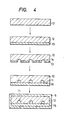
- Fig. l is a perspective view of the first embodiment of the present invention.
- a plurality of integrating circuit chips l such as LSI chips, are mounted on a wiring substrate 2, and covered with a seal cap 3.
- Pins 4 are provided on the surface of the wiring substrate 2 opposite to the integrated circuit chips l, these pins 4 and integrated circuit chips l being electrically connected.
- a power source substrate 5 has a structure in which insulating layers 6 and conductor layers 7, are laminated alternately, and bonded together to form a single unit.
- the example of the power source substrate 5 in Fig. l has eight electrically insulating layers 6 and seven feeding conductor layers 7.
- the power source substrate 5 is provided with through holes 8 into which the terminal pins 4 on the wiring substrate 2 are to be inserted.
- an electric current is supplied from an external power source device (not shown) to the power source substrate 5, and then from the feeding conductor layers 7 in the power source substrate 5 to the integrated circuit chips l through the terminal pins 4 on the wiring substrate 2.
- the power substrate 5 has an internal heat radiating structure.
- Preferred heat radiating structures will now be described with reference to Figs. 2-l0.
- Figs. 2-l0 except Fig. 6 are sectional views taken along the portions of heat radiating structures which correspond to the portion shown by the line X-X in Fig. l.
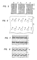
- Fig. 2 shows an example of the heat radiating structure, in which a filler l0 consisting of powder or short fibers is mixed as a heat radiating means in electrically insulating layers 6.
- a concrete example of this type of electrically insulating layer is formed by molding a plate out of a mixture of an organic resin, such as epoxy resin and the powder of a ceramic material, such as alumina.
- the particle size shall be set not larger than the thickness of the electrically insulating layer.
- the diameter of a fiber shall, of course, be set not larger than the thickness of the same layer.
- the length of the fiber may be arbitrarily set.
- the thickness of the electrically insulating layer 6 may be around l00-300 ⁇ m, and the thickness of the feeding conductor layer 7 around 200-400 ⁇ m.
- Reference numeral 8 denotes through holes into which the terminal pins 4 shown in Fig. l are inserted.
- Fig. 9 is a sectional view of a part of a power source substrate having powdered filler l0 in the electrically insulating layers 6, and Fig. l0 shows an example of the heat radiating structure in which a filler l0 of short fibers instead of powder is mixed in the electrically insulating layers 6. Referring to Figs. 9 and l0, the same reference numerals as in Fig. 2 designate the same parts.
- Fig. 3 shows an example of the heat radiating structure in which minute bores ll are formed in the feeding conductor layers to furnish the same layers with the heat radiating functions.
- These bores ll can be formed by utilizing the photoetching techniques.
- the bores ll can sufficiently function if they have a radius of 80-l20 ⁇ m.
- the shape of these bores is not specially restricted. They may be made circular or semicircular.
- the distance between adjacent bores is preferably set to l-2 mm.
- a power source substrate is formed by alternately laminating the filler-containing electrically insulating layers 6 shown in Fig. 2 and the bore-carrying feeding conductor layers 7 shown in Fig. 3.
- Fig. 4 illustrates an example of a method of forming the semicircular bores ll shown in Fig. 3, by the photoetching techniques.
- a bonding alloy film l3 is formed by deposition on one surface of a conductor plate l2 consisting of a copper plate.
- the conductor plate l2 consists of copper or a copper alloy
- the thickness of the bonding alloy film l3 may be around 2-3 ⁇ m.
- grooves l4 are then formed by photoetching. After the grooves l4 have been formed, a conductor plate l5 identical with the conductor plate l2 or some other type of conductor plate l5 having excellent conductivity is laminated on the bonding alloy film l3.
- the material for this conductor plate l5 is selected from the materials which can be bonded to the conductor plate l2 via the bonding alloy film l3. To be concrete, a material identical with that of which the conductor plate l2 is made may be used. These parts are then heated in a vacuum furnace to bond the conductor plate l2 to the conductor plate l5 via the bonding alloy film l3 and thereby combine them unitary.
- the bonding alloy film l3 is diffused into the interior of the conductors l2, l5 while it is heated under vacuum, and it substantially disappears in a final stage of the heating operation from the interface between the same conductors.
- the outer surfaces of the conductor plates l2, l5 are then coated with an organic resin, such as epoxy resin, whereby an electrically insulating layer 6 can be formed.
- the methods of coating the outer surfaces of the conductor plates l2, l5 include a method practiced by dissolving, for example, epoxy resin in acetone, applying the resultant solution to the conductor plates, and thereafter heating the resultant product at 80° - l00°C for l0-20 minutes so as to remove the acetone, the solvent.
- the feeding conductor layer and electrically insulating layer are thus combined unitary. A plurality of such unitary combined products are then laminated and heated under pressure for several hours. Thus, a power source substrate having a desired laminated structure can be manufactured.
- Fig. 5 is a sectioned front elevation of a power source substrate having through bores l6 extending in the direction of the thickness thereof, i.e., in the direction which is at right angles to the direction of extension of each of the laminated electrically insulating layers 6 and feeding conductor layers 7 in this power source substrate 5.
- Fig. 6 is a plan view of a power source substrate having through bores l6. In this case, it is necessary that heat radiating means be also provided in at least the electrically insulating layers 6 or the feeding conductor layers 7.
- the generation of heat in the power source substrate can further be suppressed by sending a gas, such as the air by a blower, or a liquid, such as water from the lower side thereof, i.e. the side thereof which is not adjacent to a wiring substrate into the through bores l6.
- the power source substrate thus formed is capable of suppressing a temperature increase by 20-30% as compared with a power source substrate which is not provided with the through bores l6.
- the number of the feeding conductor layers 7 can be regulated arbitrarily in accordance with the scale of integration of the chips.
- the thickness of the feeding conductor layer or electrically insulating layer can also be regulated arbitrarily.
- a means for supplying a coolant to the bores ll shown in Fig. 3 or the through bores l6 shown in Figs. 5 and 6 may also be selected arbitrarily, and is not specially limited.
- the filter used as the heat radiating means for the electrically insulating layers consists preferably of a powdered material or fibers. When a powdered material is used, the particle size shall be set not larger than the thickness of the electrically insulating layer.
- the filler-mixed electrically insulating layer was manufactured in the following manner.
- BF3 monoethyl amine 4 parts by weight of BF3 monoethyl amine was mixed with l00 parts by weight of epoxy resin, and alumina powder having a particle size of about 30 ⁇ m was then mixed with this mixture so that the weight of the alumina powder occupied 30% of a total weight of the resultant mixture.
- the acetone was added to this mixture to dissolve the organic resin therein, and the resultant mixture was applied to a feeding conductor plate of copper.
- the resultant product was heated at about 80°C for l0-20 minutes to dry the same, whereby the acetone, the solvent was removed therefrom.
- the thickness of the feeding conductor plate is about 300 ⁇ m, and the thickness of the electrically insulating plate about 200 ⁇ m.
- Seven plates thus formed were laminated, and heated under a pressure of about 5 kgf/cm2, at a temperature of l20°C for 4 hours and continuously heated at a temperature of l60°C for l0 hours under the same pressure to harden the resin.
- the electrically insulating layers and feeding conductor layers were bonded to one another in very good condition. Cracks did not occur in the electrically insulating layer.
- Fig. 7 is a sectioned front elevation of a part of an example of a power source substrate, in which metal wires l7 of a high heat conductivity, for example, copper wires are inserted in the electrically insulating layers 6 of an organic resin to reduce the thermal resistance.
- These heat conductive metal wires l7 spot-contact the adjacent feeding conductor layers 7 at several positions, so that the heat accumulated in the electrically insulating layers 6 can be removed efficiently through the feeding conductor layers 7.
- the metal wires l7 in each of the electrically insulating layers 6 should be disposed in contact with only one of the adjacent feeding conductor layers 7. If the metal wires l7 in the same electrically insulating layer are disposed in contact with both of the adjacent feeding conductor layers, short-circuiting occurs. Therefore, disposing the wires l7 in this manner should be avoided.
- Fig. 8 shows an example of a power source substrate, in which elongated metallic fibers l8 having a high heat conductivity and molded to a wavy shape are buried in the electrically insulating layers 6. This structure can also obtain the same heat radiating effect as the example of Fig. 7. It is also possible that molding a plurality of elongated metallic fibers to a wavy shape be done after they have been bundled up.
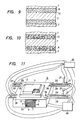
- Fig. ll is a schematic diagram of the integrated circuit device according to the present invention connected to an external power source means.
- a plurality of integrated circuit chips, such as LSI chips are mounted on a wiring substrate 2 and covered with a seal cap 3.
- the wiring substrate 2 and a power source substrate 5 are connected electrically by terminal pins (not shown).
- the power source substrate 5 is formed by laminating electrically insulating layers 6 and feeding conductor layers 7 alternately and combining them unitary.
- the example of Fig. ll is provided with five electrically insulating layers 6 and four feeding conductor layers 7.
- Coolant flow passages 20 are formed in the feeding conductor layers 7 in the power source substrate 5.
- the supplying of an electric current from an external power source means 30 to the feeding conductor layers 7 and the supplying and discharging of a coolant to and from the same layers 7 are done via feeding connecting terminals 28 and conductors 29.
- Reference numeral 25 denotes a coolant tank, the coolant in which is supplied to coolant inlet ports 27 provided at predetermined portions of the conductors 29.
- the feeding connecting terminals 28 will now be described with reference to Figs. l2, l3 and l4.
- Fig. l2 is a perspective view illustrating the construction of the joint portions of a terminal pin 35 of a feeding connecting terminal 28 and a connector 40 in a power source substrate 5.
- the pin 35 is provided with a coolant passage 3l so that a coolant flows from the coolant tank thereinto.
- the pin 35 and the external power source means 30 and coolant tank 25 are connected together by conductors 29 extending from the pins 35.
- the coolant flowing in the coolant passage 3l is supplied thereinto from the coolant tank 25 and via a coolant inlet port 27 provided at a predetermined portion of a conductor 29.
- the connector 40 is formed in the power source substrate 5.
- An insulated layer 4l is formed on the inner surface of the connector 40 except the portion of the same inner surface which corresponds to a conductor layer 7a into which an electric current and coolant are introduced via the feeding connecting terminal 28.
- the introduction of the coolant from the feeding connecting terminal to the conductor layer 7a is done by sending the coolant into the coolant passage 20 in the conductor layer 7a through the coolant passage 3l.
- Fig. l4 shows another example of the feeding connecting terminal 28.
- This connecting terminal 28 is inserted in a hose 50 of Teflon so that a coolant flows in a space between the outer surface of the connecting terminal 28 and the inner surface of the hose 50.
- the structure for connecting the power source substrate to the external power source means is not limited to the structure described above.
- the coolant be also supplied into the cables by which the external power source means 30 and conductors 29 are connected.
- the connectors 40 in the feeding conductor layers 7 in the power source substrate and through holes 8 can be formed by a boring operation utilizing the thermal energy including a laser beam or an electron beam, or a boring operation using mechanical tools.
- an electrically insulating layer may be provided on the inner surface of each thereof in the same manner as in the production of the connectors 40. However, it is necessary that such an electrically insulating layer is not formed on the inner surface of each through hole in the feeding conductor layers which are connected electrically to the terminal pins 4 on the wiring substrate 2.
- the heat radiating capability of the power source substrate can be improved markedly, and the integrated circuit chips can be mounted with a high density on a wiring substrate in an integrated circuit device.
- the electrically insulating layers are formed of an organic resin and a heat conductive filler, a compact integrated circuit device can be obtained.
- the integrated circuit device can be made compact as compared with an integrated circuit device in which the supplying of an electric current and coolant is done separately. If the integrated circuit device is formed in this manner, the conductors between the external power source means and feeding connecting terminals are also cooled, so that an increase in the temperature in the integrated circuit device can further be reduced.
Landscapes
- Engineering & Computer Science (AREA)
- Microelectronics & Electronic Packaging (AREA)
- Cooling Or The Like Of Semiconductors Or Solid State Devices (AREA)
- Production Of Multi-Layered Print Wiring Board (AREA)
Applications Claiming Priority (4)
| Application Number | Priority Date | Filing Date | Title |
|---|---|---|---|
| JP280960/85 | 1985-12-16 | ||
| JP60280960A JPS62140448A (ja) | 1985-12-16 | 1985-12-16 | 集積回路装置 |
| JP61130120A JPS62287698A (ja) | 1986-06-06 | 1986-06-06 | 集積回路装置 |
| JP130120/86 | 1986-06-06 |
Publications (3)
| Publication Number | Publication Date |
|---|---|
| EP0228212A2 true EP0228212A2 (fr) | 1987-07-08 |
| EP0228212A3 EP0228212A3 (en) | 1989-09-27 |
| EP0228212B1 EP0228212B1 (fr) | 1991-08-07 |
Family
ID=26465313
Family Applications (1)
| Application Number | Title | Priority Date | Filing Date |
|---|---|---|---|
| EP86309619A Expired EP0228212B1 (fr) | 1985-12-16 | 1986-12-10 | Dispositif à circuit intégré |
Country Status (3)
| Country | Link |
|---|---|
| US (1) | US4809058A (fr) |
| EP (1) | EP0228212B1 (fr) |
| DE (1) | DE3680774D1 (fr) |
Cited By (5)
| Publication number | Priority date | Publication date | Assignee | Title |
|---|---|---|---|---|
| FR2625042A1 (fr) * | 1987-12-22 | 1989-06-23 | Thomson Csf | Structure microelectronique hybride modulaire a haute densite d'integration |
| EP0298211A3 (fr) * | 1987-07-06 | 1991-01-16 | International Business Machines Corporation | Assemblage de cartes de circuits imprimés en céramique avec distribution de puissance et système de refroidissement |
| GB2242069A (en) * | 1990-03-08 | 1991-09-18 | Nobuo Mikoshiba | Arrangement for cooling a semiconductor element |
| EP0456423A3 (en) * | 1990-05-11 | 1992-08-26 | American Telephone And Telegraph Company | Circuit pack with inboard jet cooling |
| EP0367630B1 (fr) * | 1988-11-02 | 1996-03-13 | Fujitsu Limited | Empaquetage pour dispositifs électroniques fonctionnant à températures respectives différentes |
Families Citing this family (17)
| Publication number | Priority date | Publication date | Assignee | Title |
|---|---|---|---|---|
| US4901136A (en) * | 1987-07-14 | 1990-02-13 | General Electric Company | Multi-chip interconnection package |
| US4922325A (en) * | 1987-10-02 | 1990-05-01 | American Telephone And Telegraph Company | Multilayer ceramic package with high frequency connections |
| JP2610487B2 (ja) * | 1988-06-10 | 1997-05-14 | 株式会社日立製作所 | セラミック積層回路基板 |
| JP2760829B2 (ja) * | 1989-01-13 | 1998-06-04 | 株式会社日立製作所 | 電子基板 |
| US4998803A (en) * | 1989-04-13 | 1991-03-12 | Tacan Corporation | Mounting structure for optical and electro-optical components and method of making same |
| US5200810A (en) * | 1990-04-05 | 1993-04-06 | General Electric Company | High density interconnect structure with top mounted components |
| US5068715A (en) * | 1990-06-29 | 1991-11-26 | Digital Equipment Corporation | High-power, high-performance integrated circuit chip package |
| US5105429A (en) * | 1990-07-06 | 1992-04-14 | The United States Of America As Represented By The Department Of Energy | Modular package for cooling a laser diode array |
| JP2501266B2 (ja) * | 1991-11-15 | 1996-05-29 | 株式会社東芝 | 半導体モジュ―ル |
| US5509468A (en) * | 1993-12-23 | 1996-04-23 | Storage Technology Corporation | Assembly for dissipating thermal energy contained in an electrical circuit element and associated method therefor |
| JP3319975B2 (ja) * | 1997-05-08 | 2002-09-03 | 株式会社日立製作所 | 半導体素子及びそれを用いた液晶表示装置 |
| US6377457B1 (en) * | 2000-09-13 | 2002-04-23 | Intel Corporation | Electronic assembly and cooling thereof |
| IT1404136B1 (it) * | 2010-10-19 | 2013-11-15 | Cedal Equipment S R L | "metodo ed apparecchiatura per la saldatura di circuiti stampati" |
| WO2015018443A1 (fr) * | 2013-08-07 | 2015-02-12 | Abb S.P.A. | Appareil de refroidissement pour un dispositif électrique ou électronique et dispositif électrique ou électronique, en particulier un disjoncteur, comprenant ledit appareil de refroidissement |
| US10375901B2 (en) | 2014-12-09 | 2019-08-13 | Mtd Products Inc | Blower/vacuum |
| TWI578872B (zh) * | 2015-07-22 | 2017-04-11 | 乾坤科技股份有限公司 | 印刷電路板之多層導線結構、磁性元件及其製造方法 |
| TWI579987B (zh) * | 2015-12-22 | 2017-04-21 | 財團法人工業技術研究院 | 散熱模組 |
Family Cites Families (10)
| Publication number | Priority date | Publication date | Assignee | Title |
|---|---|---|---|---|
| US2501331A (en) * | 1947-02-24 | 1950-03-21 | Westinghouse Electric Corp | Liquid-cooled rectifier assembly |
| FR1319387A (fr) * | 1962-01-17 | 1963-03-01 | Chausson Usines Sa | Procédé et dispositif pour le refroidissement d'éléments semi-conducteurs, notamment de transistors |
| FR1481645A (fr) * | 1966-05-31 | 1967-05-19 | Trane Co | échangeur de chaleur |
| US3512582A (en) * | 1968-07-15 | 1970-05-19 | Ibm | Immersion cooling system for modularly packaged components |
| JPS55162249A (en) * | 1979-06-04 | 1980-12-17 | Hitachi Ltd | Heat discharge electrode plate for ic device |
| DE3133485A1 (de) * | 1980-09-15 | 1982-05-06 | Peter 2563 Ipsach Herren | Fluessigkeitsgekuehlte elektrische baugruppe |
| JPS5879755A (ja) * | 1981-11-06 | 1983-05-13 | Fujitsu Ltd | 半導体装置 |
| JPS5998541A (ja) * | 1982-11-26 | 1984-06-06 | Hitachi Ltd | 半導体モジユ−ル |
| JPS59202654A (ja) * | 1983-05-02 | 1984-11-16 | Nippon Telegr & Teleph Corp <Ntt> | 集積回路パツケ−ジ |
| US4631636A (en) * | 1984-03-26 | 1986-12-23 | Harris Corporation | High density packaging technique for electronic systems |
-
1986
- 1986-12-10 DE DE8686309619T patent/DE3680774D1/de not_active Expired - Lifetime
- 1986-12-10 EP EP86309619A patent/EP0228212B1/fr not_active Expired
- 1986-12-15 US US06/941,812 patent/US4809058A/en not_active Expired - Fee Related
Cited By (9)
| Publication number | Priority date | Publication date | Assignee | Title |
|---|---|---|---|---|
| EP0298211A3 (fr) * | 1987-07-06 | 1991-01-16 | International Business Machines Corporation | Assemblage de cartes de circuits imprimés en céramique avec distribution de puissance et système de refroidissement |
| FR2625042A1 (fr) * | 1987-12-22 | 1989-06-23 | Thomson Csf | Structure microelectronique hybride modulaire a haute densite d'integration |
| EP0325068A1 (fr) * | 1987-12-22 | 1989-07-26 | Thomson-Csf | Structure microélectronique hybride modulaire à haute densité d'intégration |
| US4958258A (en) * | 1987-12-22 | 1990-09-18 | Thomson-Csf | Modular hybrid microelectronic structures with high density of integration |
| EP0367630B1 (fr) * | 1988-11-02 | 1996-03-13 | Fujitsu Limited | Empaquetage pour dispositifs électroniques fonctionnant à températures respectives différentes |
| GB2242069A (en) * | 1990-03-08 | 1991-09-18 | Nobuo Mikoshiba | Arrangement for cooling a semiconductor element |
| US5262673A (en) * | 1990-03-08 | 1993-11-16 | Nobuo Mikoshiba | Semiconductor element |
| GB2242069B (en) * | 1990-03-08 | 1994-02-23 | Nobuo Mikoshiba | Semiconductor element |
| EP0456423A3 (en) * | 1990-05-11 | 1992-08-26 | American Telephone And Telegraph Company | Circuit pack with inboard jet cooling |
Also Published As
| Publication number | Publication date |
|---|---|
| US4809058A (en) | 1989-02-28 |
| DE3680774D1 (de) | 1991-09-12 |
| EP0228212B1 (fr) | 1991-08-07 |
| EP0228212A3 (en) | 1989-09-27 |
Similar Documents
| Publication | Publication Date | Title |
|---|---|---|
| EP0228212A2 (fr) | Dispositif à circuit intégré | |
| US4970577A (en) | Semiconductor chip module | |
| US8007897B2 (en) | Insulating sheet and method for producing it, and power module comprising the insulating sheet | |
| AU648412B2 (en) | Three-dimensional multichip module systems and methods of fabrication | |
| CA1257402A (fr) | Systeme et boitier d'interconnexion de puces | |
| US5270571A (en) | Three-dimensional package for semiconductor devices | |
| US5419038A (en) | Method for fabricating thin-film interconnector | |
| US5590030A (en) | Circuit board capable of efficiently conducting heat through an inside thereof using thermal lands surrounding through-hole connections | |
| EP0399161B1 (fr) | Structure de circuit multicouche | |
| US5435057A (en) | Interconnection method and structure for organic circuit boards | |
| US5286927A (en) | Method of manufacturing circuit board and circuit board itself manufactured by said method | |
| JP3588230B2 (ja) | 配線基板の製造方法 | |
| EP0332559A2 (fr) | Procédé de fabrication d'un substrat pour supporter et connecter électriquement des composants électroniques | |
| EP0645952A1 (fr) | Procédé de fabrication d'un circuit multicouche | |
| EP0349756A2 (fr) | Méthode de fabrication de dispositif de circuit électrique | |
| JPH0533557B2 (fr) | ||
| EP0875936A2 (fr) | Substrat d'interconnexion ayant des traversées | |
| WO1992003034A1 (fr) | Systeme de panneaux en materiau composite metallique ceramique thermoconducteur ameliorant la dissipation de chaleur | |
| US7407836B2 (en) | High-voltage module and method for producing same | |
| US5050036A (en) | Liquid cooled integrated circuit assembly | |
| EP0926931B1 (fr) | Tableau de connexions a trous d'interconnexion | |
| US5819858A (en) | Circuit board having a metal matrix composite inlay | |
| US3837074A (en) | Coaxial interconnections | |
| US20190244872A1 (en) | Layered cooling structure including insulative layer and multiple metallization layers | |
| JP2025521899A (ja) | 高周波発生器 |
Legal Events
| Date | Code | Title | Description |
|---|---|---|---|
| PUAI | Public reference made under article 153(3) epc to a published international application that has entered the european phase |
Free format text: ORIGINAL CODE: 0009012 |
|
| 17P | Request for examination filed |
Effective date: 19870130 |
|
| AK | Designated contracting states |
Kind code of ref document: A2 Designated state(s): DE FR GB |
|
| PUAL | Search report despatched |
Free format text: ORIGINAL CODE: 0009013 |
|
| RHK1 | Main classification (correction) |
Ipc: H05K 7/20 |
|
| AK | Designated contracting states |
Kind code of ref document: A3 Designated state(s): DE FR GB |
|
| 17Q | First examination report despatched |
Effective date: 19900118 |
|
| GRAA | (expected) grant |
Free format text: ORIGINAL CODE: 0009210 |
|
| AK | Designated contracting states |
Kind code of ref document: B1 Designated state(s): DE FR GB |
|
| REF | Corresponds to: |
Ref document number: 3680774 Country of ref document: DE Date of ref document: 19910912 |
|
| ET | Fr: translation filed | ||
| PLBE | No opposition filed within time limit |
Free format text: ORIGINAL CODE: 0009261 |
|
| STAA | Information on the status of an ep patent application or granted ep patent |
Free format text: STATUS: NO OPPOSITION FILED WITHIN TIME LIMIT |
|
| 26N | No opposition filed | ||
| PGFP | Annual fee paid to national office [announced via postgrant information from national office to epo] |
Ref country code: FR Payment date: 19931119 Year of fee payment: 8 |
|
| PGFP | Annual fee paid to national office [announced via postgrant information from national office to epo] |
Ref country code: GB Payment date: 19931130 Year of fee payment: 8 |
|
| PGFP | Annual fee paid to national office [announced via postgrant information from national office to epo] |
Ref country code: DE Payment date: 19940228 Year of fee payment: 8 |
|
| PG25 | Lapsed in a contracting state [announced via postgrant information from national office to epo] |
Ref country code: GB Effective date: 19941210 |
|
| GBPC | Gb: european patent ceased through non-payment of renewal fee |
Effective date: 19941210 |
|
| PG25 | Lapsed in a contracting state [announced via postgrant information from national office to epo] |
Ref country code: FR Effective date: 19950831 |
|
| PG25 | Lapsed in a contracting state [announced via postgrant information from national office to epo] |
Ref country code: DE Effective date: 19950901 |
|
| REG | Reference to a national code |
Ref country code: FR Ref legal event code: ST |