EP0228869A2 - Verfahren zur Herstellung eines Gehäuses für ein elektronisches Bauelement - Google Patents
Verfahren zur Herstellung eines Gehäuses für ein elektronisches Bauelement Download PDFInfo
- Publication number
- EP0228869A2 EP0228869A2 EP86309867A EP86309867A EP0228869A2 EP 0228869 A2 EP0228869 A2 EP 0228869A2 EP 86309867 A EP86309867 A EP 86309867A EP 86309867 A EP86309867 A EP 86309867A EP 0228869 A2 EP0228869 A2 EP 0228869A2
- Authority
- EP
- European Patent Office
- Prior art keywords
- leads
- lead frame
- level
- component
- lead
- Prior art date
- Legal status (The legal status is an assumption and is not a legal conclusion. Google has not performed a legal analysis and makes no representation as to the accuracy of the status listed.)
- Granted
Links
Images


Classifications
-
- H—ELECTRICITY
- H10—SEMICONDUCTOR DEVICES; ELECTRIC SOLID-STATE DEVICES NOT OTHERWISE PROVIDED FOR
- H10W—GENERIC PACKAGES, INTERCONNECTIONS, CONNECTORS OR OTHER CONSTRUCTIONAL DETAILS OF DEVICES COVERED BY CLASS H10
- H10W74/00—Encapsulations, e.g. protective coatings
- H10W74/10—Encapsulations, e.g. protective coatings characterised by their shape or disposition
- H10W74/111—Encapsulations, e.g. protective coatings characterised by their shape or disposition the semiconductor body being completely enclosed
-
- H—ELECTRICITY
- H10—SEMICONDUCTOR DEVICES; ELECTRIC SOLID-STATE DEVICES NOT OTHERWISE PROVIDED FOR
- H10W—GENERIC PACKAGES, INTERCONNECTIONS, CONNECTORS OR OTHER CONSTRUCTIONAL DETAILS OF DEVICES COVERED BY CLASS H10
- H10W70/00—Package substrates; Interposers; Redistribution layers [RDL]
- H10W70/40—Leadframes
- H10W70/411—Chip-supporting parts, e.g. die pads
-
- H—ELECTRICITY
- H10—SEMICONDUCTOR DEVICES; ELECTRIC SOLID-STATE DEVICES NOT OTHERWISE PROVIDED FOR
- H10W—GENERIC PACKAGES, INTERCONNECTIONS, CONNECTORS OR OTHER CONSTRUCTIONAL DETAILS OF DEVICES COVERED BY CLASS H10
- H10W70/00—Package substrates; Interposers; Redistribution layers [RDL]
- H10W70/40—Leadframes
- H10W70/421—Shapes or dispositions
- H10W70/442—Shapes or dispositions of multiple leadframes in a single chip
-
- H—ELECTRICITY
- H10—SEMICONDUCTOR DEVICES; ELECTRIC SOLID-STATE DEVICES NOT OTHERWISE PROVIDED FOR
- H10W—GENERIC PACKAGES, INTERCONNECTIONS, CONNECTORS OR OTHER CONSTRUCTIONAL DETAILS OF DEVICES COVERED BY CLASS H10
- H10W74/00—Encapsulations, e.g. protective coatings
- H10W74/10—Encapsulations, e.g. protective coatings characterised by their shape or disposition
-
- H—ELECTRICITY
- H10—SEMICONDUCTOR DEVICES; ELECTRIC SOLID-STATE DEVICES NOT OTHERWISE PROVIDED FOR
- H10W—GENERIC PACKAGES, INTERCONNECTIONS, CONNECTORS OR OTHER CONSTRUCTIONAL DETAILS OF DEVICES COVERED BY CLASS H10
- H10W90/00—Package configurations
- H10W90/701—Package configurations characterised by the relative positions of pads or connectors relative to package parts
- H10W90/751—Package configurations characterised by the relative positions of pads or connectors relative to package parts of bond wires
- H10W90/756—Package configurations characterised by the relative positions of pads or connectors relative to package parts of bond wires between a chip and a stacked lead frame, conducting package substrate or heat sink
-
- Y—GENERAL TAGGING OF NEW TECHNOLOGICAL DEVELOPMENTS; GENERAL TAGGING OF CROSS-SECTIONAL TECHNOLOGIES SPANNING OVER SEVERAL SECTIONS OF THE IPC; TECHNICAL SUBJECTS COVERED BY FORMER USPC CROSS-REFERENCE ART COLLECTIONS [XRACs] AND DIGESTS
- Y10—TECHNICAL SUBJECTS COVERED BY FORMER USPC
- Y10T—TECHNICAL SUBJECTS COVERED BY FORMER US CLASSIFICATION
- Y10T29/00—Metal working
- Y10T29/49—Method of mechanical manufacture
- Y10T29/49002—Electrical device making
- Y10T29/49117—Conductor or circuit manufacturing
- Y10T29/49121—Beam lead frame or beam lead device
Definitions
- This invention relates to electronic component packages and in particular to packaging semiconductor chips which require a high density of external electrical connections.
- the lead frame may be visualized as a solid metal picture frame with slender fingers radiating inward from either two opposing sides or from all four sides toward the geometric center of the picture frame. Also radiating inward from each of the four corners of the picture frame is a slender finger which terminates on a square or rectangular piece of metal, typically referred to as a paddle, which occupies a portion of the area around the geometric center.
- the chip is first epoxied to the paddle and then electrically connected to the lead frame by wire bonds which originate at the contact pads on the chip and terminate on the fingers.
- the lead frame fingers stop short of contacting the paddle in order to electrically isolate the two entities.
- the chip and a portion of the lead frame fingers are then encapsulated, or molded, in a material such as an epoxy or plastic molding compound. Finally, the molded package body and lead frame fingers are excised from the metal picture frame portion of the lead frame.
- An encapsulated electronic component package comprises an electronic component, a first level of conductive leads electrically coupled to associated contact areas on the component, and a second level of conductive leads disposed above the leads of the first level in an area proximate to said component and electrically coupled to associated contact areas on the component, said leads extending from an area proximate to said component to an area outside the encapsulant.
- An electronic component such as a standard silicon semiconductor chip, l0, which in this example is a microprocessor chip, was mounted on a paddle, ll, which makes electrical contact to the back side of the chip.
- the paddle is part of a lower lead frame, l2 (see FIG. 3), which also includes a plurality of leads such as l3 and l4 radiating inward from the solid picture-frame-like perimeter to the vicinity of the chip.
- the lower lead frame has leads extending to all four sides of the chip, but the invention is also applicable to packages where the leads extend to only one side or two sides of the chip, generally known in the art as single-in-line and dual-in-line packages, respectively. Of course, packages with leads extending to all four sides (quad packages) provide the maximum density of external electrical connection.
- the package further includes an upper lead frame, l5, with leads such as l6 and l7, radiating inward from the said picture-frame-like perimeter to the area proximate the chip, though generally not as far as the leads, l3 and l4, of the lower lead frame.
- the leads of the upper lead frame lie above the leads of the lower lead frame at least in the area proximate to the chip.
- the leads of the upper lead frame are also preferably interdigitated with those of the lower lead frame, i.e., the upper leads lie in the spaces between the lower leads though in a higher plane.
- the leads of both lead frames are self-supporting as is typical in molded plastic assemblies. That is, the leads are not deposited on any material or substrate and maintain their individual positions and shape without any support other than the lead frame itself. However, it is desirable to insure that the upper and lower leads remain physically separate and so spacers, l8 and l9, of an insulating material are provided essentially parallel to each side of the chip between the upper and lower leads.
- the spacers were strips of a double-sided adhesive insulating tape, such as that sold by Amicon under the designation TG-86, which were placed on the leads of the lower lead frame.
- the upper surface of the chip, l0 includes a plurality of contact areas or bond pads, depicted as 20, 2l, and 29, that are typically distributed along all four sides of the device. These contact areas are electrically interconnected to the chip circuitry by means of metallized runners (not shown) and serve as the point of external electrical connection to the circuitry. Each contact area was electrically connected to one of the leads of the upper or lower lead frame by wires, such as wires 22 and 23 which connect pads 20 and 2l to leads l3 and l4, and wires 24 and 25 which connect adjacent pads to leads l6 and l7 (one of which is shown in FIG. l as pad 29).
- wires 22 and 23 which connect pads 20 and 2l to leads l3 and l4, and wires 24 and 25 which connect adjacent pads to leads l6 and l7 (one of which is shown in FIG. l as pad 29).
- the semiconductor chip and a portion of the leads were encapsulated within a standard encapsulant, 26, which in this example was an epoxy molding compound. It will be noted, as shown in FIG. 2, that a portion of the leads of the upper lead frame is made coplanar with the leads of the lower lead frame. This portion extends from an area removed from the semiconductor chip but within the encapsulant, 26, to an area extending outside the boundary of the encapsulant.
- the length of the coplanar portions will depend upon the desired length of the pins in the final package, since it is desirable to separate the leads from the lead frame along lines such as 27 and 28 in the coplanar portions to keep all pins the same length.
- FIG. 2 shows the lead frame assemblies prior to separating the leads from the frame and forming the leads into their final configuration, while FIG. l shows the completed package.
- the chip, l0 measured approximately 0.400 ⁇ 0.375 ⁇ 0.020 inches and had a different number of contact pads ranging from 22 to 43 on each side.
- Each lead had a length of approximately 0.420 inches from the perimeter to the edge near the chip and a thickness of approximately 0.006 inches.
- the coplanar portion of the upper and lower leads was approximately 0.l40 inches in length.
- the size of the package, as defined by the dimensions of the encapsulant was l.070 ⁇ l.070 ⁇ 0.ll0 inches and each lead extending from the package was 0.l00 inches long.
- the leads of the lower lead frame extended to approximately 0.02 inches from the edge of the chip (0.0l inches from the paddle edge) and the leads of the upper lead frame extended to approximately 0.05 inches from the edge of the chip (0.04 inches from the paddle).
- this package in contrast to multi-layer ceramic packages, provides electrical contacts to the chip pads by means of leads which are an integral part of the final package. That is, the leads extend from an area proximate to the chip within the encapsulant to an area outside the encapsulant where they can make contact to external circuitry such as a printed wiring board.
- This lead frame represents the lower lead frame of the package and it includes, as a mounting portion for the chip, a paddle ll which is interconnected to paddle support leads 45-48.
- the chip was mounted to the paddle by a conductive epoxy.
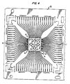
- the upper lead frame of the package appears initially as shown in FIG. 4. All the leads, such as l6 and l7, which extend from the picture-frame-like perimeter are initially tied together by tiebars 30-33 and crossbars 34 and 35. Included in the crossbars are expansion joints 36-39 to allow for possible differential motion of leads on a particular side during processing of the lead frame.
- the upper lead frame is initially flat, and the final shape (see FIG. 2) is achieved by first bending all the leads downward to the level of what will be the coplanar portions of of the final assembly. The central portion of the fingers is then bent upward in such a manner that they will be parallel to, and positioned at the desired height above, the lower lead frame. This can be done by standard metal-working techniques.
- the leads are separated from each other by punching out the central portion of the assembly which includes the tiebars, crossbars, expansion joints, and a portion of the end of each lead.
- the boundary of the cut-out portion is represented by the dashed lines 40-43. It will be appreciated that this upper lead frame can be used for a chip of any size by cutting off an appropriate length of each lead at the central region of the assembly.
- Strips of insulating material (see FIG. 2) which act as spacers, l8 and l9, can be placed on the lower lead frame of FIG. 3, before or after mounting the chip. However, in order to prevent possible damage to the chip, it is desirable to deposit the strips before mounting the chip.
- the upper lead frame of FIG. 4 is then oriented over the lower lead frame of FIG. 3 so that the leads of the upper frame are aligned with their associated contact pads on the chip while resting on the spacers at a position above the leads of the lower assembly. At the same time, the downwardly bent portions of the upper lead frame fall within the spaces of the leads of the lower lead frame.
- the upper and lower lead frames can be aligned by means of alignment markers or by means of alignment holes as shown in FIGS. 3 and 4.
- the frames While held in the aligned position, the frames are permanently fastened together at the perimeter by some means, e.g., welding, soldering, contact cement, etc., to form a lead frame assembly. Wire contacts are then formed between each contact pad and its associated lead by standard wire bonding. The assembly can then be encapsulated by standard techniques and materials such as transfer molding with an epoxy molding compound. Finally, the leads can be separated from the frame by standard cutting operations, and then formed approximately 90 degrees to provide a desired standoff height, followed by another 90 degree bend to produce the foot on which the package rests.
- some means e.g., welding, soldering, contact cement, etc.
- the invention has been described with regard to packaging a particular semiconductor chip, it will be appreciated that the concepts can be utilized for any semiconductor chip having a high density of contact areas on a side (especially for those devices with a contact pad center-to-center spacing of 0.008 inches or less).
- the invention may be used for packaging hybrid integrated circuits or other electrical components.
- additional lead frames could be provided for certain needs.
- a third lead frame functioning as a ground plane could be provided beneath the lower lead frame (l2) shown in the figures.
- a third lead frame might also be provided to further reduce the center-to-center spacing of the leads.
Landscapes
- Lead Frames For Integrated Circuits (AREA)
- Structures Or Materials For Encapsulating Or Coating Semiconductor Devices Or Solid State Devices (AREA)
Applications Claiming Priority (2)
| Application Number | Priority Date | Filing Date | Title |
|---|---|---|---|
| US816443 | 1986-01-06 | ||
| US06/816,443 US4801765A (en) | 1986-01-06 | 1986-01-06 | Electronic component package using multi-level lead frames |
Publications (3)
| Publication Number | Publication Date |
|---|---|
| EP0228869A2 true EP0228869A2 (de) | 1987-07-15 |
| EP0228869A3 EP0228869A3 (en) | 1987-09-16 |
| EP0228869B1 EP0228869B1 (de) | 1992-04-15 |
Family
ID=25220635
Family Applications (1)
| Application Number | Title | Priority Date | Filing Date |
|---|---|---|---|
| EP86309867A Expired - Lifetime EP0228869B1 (de) | 1986-01-06 | 1986-12-17 | Verfahren zur Herstellung eines Gehäuses für ein elektronisches Bauelement |
Country Status (5)
| Country | Link |
|---|---|
| US (1) | US4801765A (de) |
| EP (1) | EP0228869B1 (de) |
| JP (1) | JP2509595B2 (de) |
| DE (1) | DE3684896D1 (de) |
| ES (1) | ES2030392T3 (de) |
Cited By (11)
| Publication number | Priority date | Publication date | Assignee | Title |
|---|---|---|---|---|
| EP0295459A3 (de) * | 1987-06-15 | 1989-10-18 | International Business Machines Corporation | Elekrtronischer Zusammenbau und Verfahren zur Herstellung desselben |
| FR2647958A1 (en) * | 1989-05-30 | 1990-12-07 | Thomson Composants Militaires | Plastic housing for integrated circuit with staggered grids on two levels and method of manufacture |
| GB2237144A (en) * | 1989-10-06 | 1991-04-24 | Cabot Corp | Multilayered leadframe with interdigitated leads |
| FR2664097A1 (fr) * | 1990-06-28 | 1992-01-03 | Sgs Thomson Microelectronics | Boitier de circuit integre et son procede de fabrication. |
| EP0581588A1 (de) * | 1992-07-28 | 1994-02-02 | Shinko Electric Industries Co. Ltd. | Metallträger für ein Mehrschicht-Leitergitter und Verfahren zum Herstellen desselben |
| GB2293918A (en) * | 1994-10-06 | 1996-04-10 | Ibm | Electronic circuit packaging |
| GB2301936A (en) * | 1995-06-05 | 1996-12-18 | Samsung Aerospace Ind | Lead frames for semiconductor devices |
| GB2317989A (en) * | 1996-10-01 | 1998-04-08 | Int Rectifier Corp | Lead frames for semiconductor packages |
| US5854094A (en) * | 1992-07-28 | 1998-12-29 | Shinko Electric Industries Co., Ltd. | Process for manufacturing metal plane support for multi-layer lead frames |
| WO2001015226A1 (en) * | 1999-08-24 | 2001-03-01 | General Semiconductor, Inc. | Lead frame structure for the fabrication of hybrid semiconductor devices |
| DE102020109493A1 (de) | 2020-04-06 | 2021-10-07 | Infineon Technologies Ag | Ein halbleiterbauelementpackage mit zwei übereinander gestapelten leadframes |
Families Citing this family (34)
| Publication number | Priority date | Publication date | Assignee | Title |
|---|---|---|---|---|
| USRE36894E (en) * | 1986-05-27 | 2000-10-03 | Lucent Technologies Inc. | Semiconductor package with high density I/O lead connection |
| FR2624651B1 (fr) * | 1987-12-14 | 1991-09-06 | Sgs Thomson Microelectronics | Procede de mise en place d'un composant electronique et de ses connexions electriques sur un support et produit ainsi obtenu |
| US5099306A (en) * | 1988-11-21 | 1992-03-24 | Honeywell Inc. | Stacked tab leadframe assembly |
| JPH02156661A (ja) * | 1988-12-09 | 1990-06-15 | Mitsui High Tec Inc | リードフレームおよびその製造方法 |
| USRE35578E (en) * | 1988-12-12 | 1997-08-12 | Sgs-Thomson Microelectronics, Inc. | Method to install an electronic component and its electrical connections on a support, and product obtained thereby |
| US4912547A (en) * | 1989-01-30 | 1990-03-27 | International Business Machines Corporation | Tape bonded semiconductor device |
| US5089878A (en) * | 1989-06-09 | 1992-02-18 | Lee Jaesup N | Low impedance packaging |
| US5025114A (en) * | 1989-10-30 | 1991-06-18 | Olin Corporation | Multi-layer lead frames for integrated circuit packages |
| US5159750A (en) * | 1989-12-20 | 1992-11-03 | National Semiconductor Corporation | Method of connecting an IC component with another electrical component |
| US5147815A (en) * | 1990-05-14 | 1992-09-15 | Motorola, Inc. | Method for fabricating a multichip semiconductor device having two interdigitated leadframes |
| US5227583A (en) * | 1991-08-20 | 1993-07-13 | Microelectronic Packaging America | Ceramic package and method for making same |
| US5403784A (en) * | 1991-09-03 | 1995-04-04 | Microelectronics And Computer Technology Corporation | Process for manufacturing a stacked multiple leadframe semiconductor package using an alignment template |
| US5249354A (en) * | 1991-09-25 | 1993-10-05 | American Telephone & Telegraph Co. | Method of making electronic component packages |
| JPH05190721A (ja) * | 1992-01-08 | 1993-07-30 | Fujitsu Ltd | 半導体装置及びその製造方法 |
| JPH0653277A (ja) * | 1992-06-04 | 1994-02-25 | Lsi Logic Corp | 半導体装置アセンブリおよびその組立方法 |
| US5325268A (en) * | 1993-01-28 | 1994-06-28 | National Semiconductor Corporation | Interconnector for a multi-chip module or package |
| US5598307A (en) * | 1994-04-15 | 1997-01-28 | Hutchinson Technology Inc. | Integrated gimbal suspension assembly |
| JP2955829B2 (ja) | 1994-04-15 | 1999-10-04 | ハッチンソン テクノロジー インコーポレイテッド | ヘッドサスペンション |
| US5491597A (en) * | 1994-04-15 | 1996-02-13 | Hutchinson Technology Incorporated | Gimbal flexure and electrical interconnect assembly |
| US5484097A (en) * | 1994-07-12 | 1996-01-16 | General Instrument Corp. | Fabrication of hybrid semiconductor devices |
| US6150716A (en) * | 1995-01-25 | 2000-11-21 | International Business Machines Corporation | Metal substrate having an IC chip and carrier mounting |
| WO1996031906A1 (en) * | 1995-04-05 | 1996-10-10 | National Semiconductor Corporation | Multi-layer lead frame |
| US5808834A (en) * | 1995-06-07 | 1998-09-15 | Hutchinson Technology Incorporated | Laminated adapter |
| US5742009A (en) * | 1995-10-12 | 1998-04-21 | Vlsi Technology Corporation | Printed circuit board layout to minimize the clock delay caused by mismatch in length of metal lines and enhance the thermal performance of microeletronics packages via condution through the package leads |
| KR100214544B1 (ko) * | 1996-12-28 | 1999-08-02 | 구본준 | 볼 그리드 어레이 반도체 패키지 |
| US6285324B1 (en) | 1999-09-15 | 2001-09-04 | Lucent Technologies Inc. | Antenna package for a wireless communications device |
| KR20010036142A (ko) | 1999-10-06 | 2001-05-07 | 윤종용 | 다층 리드를 갖는 반도체 칩 패키지 |
| JP3799468B2 (ja) * | 2000-01-19 | 2006-07-19 | 住友電装株式会社 | 回路板の製造方法、該方法により製造された回路板および該回路板を備えた電気接続箱 |
| JP3510838B2 (ja) * | 2000-03-24 | 2004-03-29 | 三洋電機株式会社 | 半導体装置およびその製造方法 |
| US20050146025A1 (en) * | 2001-02-26 | 2005-07-07 | John Gregory | Method of forming an opening or cavity in a substrate for receiving an electronic component |
| US7122892B2 (en) * | 2004-10-07 | 2006-10-17 | Agere Systems Inc. | Multi-chip integrated circuit module for high-frequency operation |
| USD530717S1 (en) * | 2005-04-15 | 2006-10-24 | Belkin Corporation | USB hub |
| CN109904136B (zh) | 2017-12-07 | 2024-09-13 | 恩智浦美国有限公司 | 用于具有j引线和鸥翼引线的集成电路装置的引线框 |
| US10515880B2 (en) | 2018-03-16 | 2019-12-24 | Nxp Usa, Inc | Lead frame with bendable leads |
Family Cites Families (15)
| Publication number | Priority date | Publication date | Assignee | Title |
|---|---|---|---|---|
| US3271625A (en) * | 1962-08-01 | 1966-09-06 | Signetics Corp | Electronic package assembly |
| US3676748A (en) * | 1970-04-01 | 1972-07-11 | Fuji Electrochemical Co Ltd | Frame structures for electronic circuits |
| US4105861A (en) * | 1975-09-29 | 1978-08-08 | Semi-Alloys, Inc. | Hermetically sealed container for semiconductor and other electronic devices |
| JPS55120155A (en) * | 1979-03-09 | 1980-09-16 | Nec Kyushu Ltd | Semiconductor lead frame |
| JPS57121267A (en) * | 1981-01-21 | 1982-07-28 | Toshiba Corp | Laminate type lead frame |
| US4380042A (en) * | 1981-02-23 | 1983-04-12 | Angelucci Sr Thomas L | Printed circuit lead carrier tape |
| US4496965A (en) * | 1981-05-18 | 1985-01-29 | Texas Instruments Incorporated | Stacked interdigitated lead frame assembly |
| US4477828A (en) * | 1982-10-12 | 1984-10-16 | Scherer Jeremy D | Microcircuit package and sealing method |
| US4498122A (en) * | 1982-12-29 | 1985-02-05 | At&T Bell Laboratories | High-speed, high pin-out LSI chip package |
| JPS59198744A (ja) * | 1983-04-25 | 1984-11-10 | Fujitsu Ltd | 樹脂封止型半導体装置 |
| US4602831A (en) * | 1983-09-26 | 1986-07-29 | Amp Incorporated | Electrical connector and method of making same |
| US4579404A (en) * | 1983-09-26 | 1986-04-01 | Amp Incorporated | Conductor-terminated card edge connector |
| US4677526A (en) * | 1984-03-01 | 1987-06-30 | Augat Inc. | Plastic pin grid array chip carrier |
| JPS60206144A (ja) * | 1984-03-30 | 1985-10-17 | Toshiba Corp | 半導体装置およびその製造方法 |
| US4542259A (en) * | 1984-09-19 | 1985-09-17 | Olin Corporation | High density packages |
-
1986
- 1986-01-06 US US06/816,443 patent/US4801765A/en not_active Expired - Lifetime
- 1986-12-17 DE DE8686309867T patent/DE3684896D1/de not_active Expired - Lifetime
- 1986-12-17 ES ES198686309867T patent/ES2030392T3/es not_active Expired - Lifetime
- 1986-12-17 EP EP86309867A patent/EP0228869B1/de not_active Expired - Lifetime
-
1987
- 1987-01-06 JP JP62000231A patent/JP2509595B2/ja not_active Expired - Lifetime
Cited By (15)
| Publication number | Priority date | Publication date | Assignee | Title |
|---|---|---|---|---|
| EP0295459A3 (de) * | 1987-06-15 | 1989-10-18 | International Business Machines Corporation | Elekrtronischer Zusammenbau und Verfahren zur Herstellung desselben |
| FR2647958A1 (en) * | 1989-05-30 | 1990-12-07 | Thomson Composants Militaires | Plastic housing for integrated circuit with staggered grids on two levels and method of manufacture |
| GB2237144A (en) * | 1989-10-06 | 1991-04-24 | Cabot Corp | Multilayered leadframe with interdigitated leads |
| FR2664097A1 (fr) * | 1990-06-28 | 1992-01-03 | Sgs Thomson Microelectronics | Boitier de circuit integre et son procede de fabrication. |
| US5854094A (en) * | 1992-07-28 | 1998-12-29 | Shinko Electric Industries Co., Ltd. | Process for manufacturing metal plane support for multi-layer lead frames |
| US5410180A (en) * | 1992-07-28 | 1995-04-25 | Shinko Electric Industries Co., Ltd. | Metal plane support for multi-layer lead frames and a process for manufacturing such frames |
| EP0581588A1 (de) * | 1992-07-28 | 1994-02-02 | Shinko Electric Industries Co. Ltd. | Metallträger für ein Mehrschicht-Leitergitter und Verfahren zum Herstellen desselben |
| GB2293918A (en) * | 1994-10-06 | 1996-04-10 | Ibm | Electronic circuit packaging |
| GB2301936A (en) * | 1995-06-05 | 1996-12-18 | Samsung Aerospace Ind | Lead frames for semiconductor devices |
| GB2317989A (en) * | 1996-10-01 | 1998-04-08 | Int Rectifier Corp | Lead frames for semiconductor packages |
| US6114750A (en) * | 1996-10-01 | 2000-09-05 | International Rectifier Corp. | Surface mount TO-220 package and process for the manufacture thereof |
| GB2317989B (en) * | 1996-10-01 | 2002-01-23 | Int Rectifier Corp | Surface mount to-220 package and process for the manufacture thereof |
| WO2001015226A1 (en) * | 1999-08-24 | 2001-03-01 | General Semiconductor, Inc. | Lead frame structure for the fabrication of hybrid semiconductor devices |
| US6281043B1 (en) | 1999-08-24 | 2001-08-28 | General Semiconductor, Inc. | Fabrication of hybrid semiconductor devices |
| DE102020109493A1 (de) | 2020-04-06 | 2021-10-07 | Infineon Technologies Ag | Ein halbleiterbauelementpackage mit zwei übereinander gestapelten leadframes |
Also Published As
| Publication number | Publication date |
|---|---|
| JPS62216350A (ja) | 1987-09-22 |
| EP0228869A3 (en) | 1987-09-16 |
| ES2030392T3 (es) | 1992-11-01 |
| JP2509595B2 (ja) | 1996-06-19 |
| US4801765A (en) | 1989-01-31 |
| DE3684896D1 (de) | 1992-05-21 |
| EP0228869B1 (de) | 1992-04-15 |
Similar Documents
| Publication | Publication Date | Title |
|---|---|---|
| US4801765A (en) | Electronic component package using multi-level lead frames | |
| US6175149B1 (en) | Mounting multiple semiconductor dies in a package | |
| US6297547B1 (en) | Mounting multiple semiconductor dies in a package | |
| US5953589A (en) | Ball grid array semiconductor package with solder balls fused on printed circuit board and method for fabricating the same | |
| CA1252912A (en) | Semiconductor package with high density i/o lead connection | |
| EP0272187A2 (de) | Plastikverpackung für Hochfrequenz-Halbleiteranordnungen | |
| KR900002908B1 (ko) | 수지 봉지형 반도체 장치 | |
| US4448306A (en) | Integrated circuit chip carrier | |
| EP0706213A2 (de) | Einlagiger Leiterrahmenentwurf mit Erdungsflächekapazität | |
| KR100336080B1 (ko) | 반도체 장치 및 그 제조방법 | |
| JPH05109972A (ja) | リードフレーム及び集積回路チツプのパツケージ・アセンブリ | |
| EP0408779A1 (de) | Halbleiter-Speichermodul höher Dichte | |
| EP0118237A2 (de) | Leiterrahmen für ein Halbleiterelement | |
| EP0114531B2 (de) | Bauteil mit Leiteranschluss für ein Halbleiterplättchen | |
| US6791166B1 (en) | Stackable lead frame package using exposed internal lead traces | |
| KR950014677B1 (ko) | Ic 실장장치 | |
| US6627986B2 (en) | Substrate for semiconductor device and semiconductor device fabrication using the same | |
| JP2911265B2 (ja) | 表面実装型半導体装置 | |
| US5455454A (en) | Semiconductor lead frame having a down set support member formed by inwardly extending leads within a central aperture | |
| USRE36894E (en) | Semiconductor package with high density I/O lead connection | |
| JPS61279141A (ja) | 可撓性テ−パリ−ドを有したリ−ドフレ−ムと機械的ダイ支持体の直接接続装置及び方法 | |
| JPH0517709B2 (de) | ||
| JP2504901B2 (ja) | 複数の電子部品パッケ―ジの製造方法 | |
| KR100377267B1 (ko) | 리드프레임의 칩탑재판 구조 및 그 제조 방법 | |
| JPH07122701A (ja) | 半導体装置およびその製造方法ならびにpga用リードフレーム |
Legal Events
| Date | Code | Title | Description |
|---|---|---|---|
| PUAI | Public reference made under article 153(3) epc to a published international application that has entered the european phase |
Free format text: ORIGINAL CODE: 0009012 |
|
| AK | Designated contracting states |
Kind code of ref document: A2 Designated state(s): DE ES FR GB IT NL |
|
| PUAL | Search report despatched |
Free format text: ORIGINAL CODE: 0009013 |
|
| AK | Designated contracting states |
Kind code of ref document: A3 Designated state(s): DE ES FR GB IT NL |
|
| 17P | Request for examination filed |
Effective date: 19880309 |
|
| 17Q | First examination report despatched |
Effective date: 19900621 |
|
| GRAA | (expected) grant |
Free format text: ORIGINAL CODE: 0009210 |
|
| AK | Designated contracting states |
Kind code of ref document: B1 Designated state(s): DE ES FR GB IT NL |
|
| REF | Corresponds to: |
Ref document number: 3684896 Country of ref document: DE Date of ref document: 19920521 |
|
| ET | Fr: translation filed | ||
| ITF | It: translation for a ep patent filed | ||
| REG | Reference to a national code |
Ref country code: ES Ref legal event code: FG2A Ref document number: 2030392 Country of ref document: ES Kind code of ref document: T3 |
|
| PLBE | No opposition filed within time limit |
Free format text: ORIGINAL CODE: 0009261 |
|
| STAA | Information on the status of an ep patent application or granted ep patent |
Free format text: STATUS: NO OPPOSITION FILED WITHIN TIME LIMIT |
|
| 26N | No opposition filed | ||
| PGFP | Annual fee paid to national office [announced via postgrant information from national office to epo] |
Ref country code: NL Payment date: 20001130 Year of fee payment: 15 |
|
| PGFP | Annual fee paid to national office [announced via postgrant information from national office to epo] |
Ref country code: ES Payment date: 20001204 Year of fee payment: 15 |
|
| PGFP | Annual fee paid to national office [announced via postgrant information from national office to epo] |
Ref country code: GB Payment date: 20011126 Year of fee payment: 16 |
|
| REG | Reference to a national code |
Ref country code: GB Ref legal event code: IF02 |
|
| PG25 | Lapsed in a contracting state [announced via postgrant information from national office to epo] |
Ref country code: NL Free format text: LAPSE BECAUSE OF NON-PAYMENT OF DUE FEES Effective date: 20020701 |
|
| NLV4 | Nl: lapsed or anulled due to non-payment of the annual fee |
Effective date: 20020701 |
|
| PG25 | Lapsed in a contracting state [announced via postgrant information from national office to epo] |
Ref country code: GB Free format text: LAPSE BECAUSE OF NON-PAYMENT OF DUE FEES Effective date: 20021217 |
|
| PG25 | Lapsed in a contracting state [announced via postgrant information from national office to epo] |
Ref country code: ES Free format text: LAPSE BECAUSE OF NON-PAYMENT OF DUE FEES Effective date: 20021218 |
|
| GBPC | Gb: european patent ceased through non-payment of renewal fee |
Effective date: 20021217 |
|
| REG | Reference to a national code |
Ref country code: ES Ref legal event code: FD2A Effective date: 20030113 |
|
| PGFP | Annual fee paid to national office [announced via postgrant information from national office to epo] |
Ref country code: DE Payment date: 20051212 Year of fee payment: 20 |
|
| PG25 | Lapsed in a contracting state [announced via postgrant information from national office to epo] |
Ref country code: IT Free format text: LAPSE BECAUSE OF NON-PAYMENT OF DUE FEES;WARNING: LAPSES OF ITALIAN PATENTS WITH EFFECTIVE DATE BEFORE 2007 MAY HAVE OCCURRED AT ANY TIME BEFORE 2007. THE CORRECT EFFECTIVE DATE MAY BE DIFFERENT FROM THE ONE RECORDED. Effective date: 20051217 |
|
| PGFP | Annual fee paid to national office [announced via postgrant information from national office to epo] |
Ref country code: FR Payment date: 20051219 Year of fee payment: 20 |