EP0229362A2 - Halbleitervorrichtung und Methode zur Herstellung - Google Patents
Halbleitervorrichtung und Methode zur Herstellung Download PDFInfo
- Publication number
- EP0229362A2 EP0229362A2 EP86117777A EP86117777A EP0229362A2 EP 0229362 A2 EP0229362 A2 EP 0229362A2 EP 86117777 A EP86117777 A EP 86117777A EP 86117777 A EP86117777 A EP 86117777A EP 0229362 A2 EP0229362 A2 EP 0229362A2
- Authority
- EP
- European Patent Office
- Prior art keywords
- window
- layer
- region
- wafer
- insulating layer
- Prior art date
- Legal status (The legal status is an assumption and is not a legal conclusion. Google has not performed a legal analysis and makes no representation as to the accuracy of the status listed.)
- Granted
Links
Images


Classifications
-
- H—ELECTRICITY
- H10—SEMICONDUCTOR DEVICES; ELECTRIC SOLID-STATE DEVICES NOT OTHERWISE PROVIDED FOR
- H10D—INORGANIC ELECTRIC SEMICONDUCTOR DEVICES
- H10D30/00—Field-effect transistors [FET]
- H10D30/01—Manufacture or treatment
- H10D30/021—Manufacture or treatment of FETs having insulated gates [IGFET]
- H10D30/028—Manufacture or treatment of FETs having insulated gates [IGFET] of double-diffused metal oxide semiconductor [DMOS] FETs
- H10D30/0291—Manufacture or treatment of FETs having insulated gates [IGFET] of double-diffused metal oxide semiconductor [DMOS] FETs of vertical DMOS [VDMOS] FETs
-
- H—ELECTRICITY
- H10—SEMICONDUCTOR DEVICES; ELECTRIC SOLID-STATE DEVICES NOT OTHERWISE PROVIDED FOR
- H10D—INORGANIC ELECTRIC SEMICONDUCTOR DEVICES
- H10D12/00—Bipolar devices controlled by the field effect, e.g. insulated-gate bipolar transistors [IGBT]
- H10D12/01—Manufacture or treatment
- H10D12/031—Manufacture or treatment of IGBTs
- H10D12/032—Manufacture or treatment of IGBTs of vertical IGBTs
-
- H—ELECTRICITY
- H10—SEMICONDUCTOR DEVICES; ELECTRIC SOLID-STATE DEVICES NOT OTHERWISE PROVIDED FOR
- H10D—INORGANIC ELECTRIC SEMICONDUCTOR DEVICES
- H10D62/00—Semiconductor bodies, or regions thereof, of devices having potential barriers
- H10D62/10—Shapes, relative sizes or dispositions of the regions of the semiconductor bodies; Shapes of the semiconductor bodies
- H10D62/17—Semiconductor regions connected to electrodes not carrying current to be rectified, amplified or switched, e.g. channel regions
- H10D62/393—Body regions of DMOS transistors or IGBTs
-
- H—ELECTRICITY
- H10—SEMICONDUCTOR DEVICES; ELECTRIC SOLID-STATE DEVICES NOT OTHERWISE PROVIDED FOR
- H10P—GENERIC PROCESSES OR APPARATUS FOR THE MANUFACTURE OR TREATMENT OF DEVICES COVERED BY CLASS H10
- H10P32/00—Diffusion of dopants within, into or out of wafers, substrates or parts of devices
- H10P32/10—Diffusion of dopants within, into or out of semiconductor bodies or layers
- H10P32/14—Diffusion of dopants within, into or out of semiconductor bodies or layers within a single semiconductor body or layer in a solid phase; between different semiconductor bodies or layers, both in a solid phase
- H10P32/1408—Diffusion of dopants within, into or out of semiconductor bodies or layers within a single semiconductor body or layer in a solid phase; between different semiconductor bodies or layers, both in a solid phase from or through or into an external applied layer, e.g. photoresist or nitride layers
- H10P32/141—Diffusion of dopants within, into or out of semiconductor bodies or layers within a single semiconductor body or layer in a solid phase; between different semiconductor bodies or layers, both in a solid phase from or through or into an external applied layer, e.g. photoresist or nitride layers the applied layer comprising oxides only
-
- H—ELECTRICITY
- H10—SEMICONDUCTOR DEVICES; ELECTRIC SOLID-STATE DEVICES NOT OTHERWISE PROVIDED FOR
- H10P—GENERIC PROCESSES OR APPARATUS FOR THE MANUFACTURE OR TREATMENT OF DEVICES COVERED BY CLASS H10
- H10P32/00—Diffusion of dopants within, into or out of wafers, substrates or parts of devices
- H10P32/10—Diffusion of dopants within, into or out of semiconductor bodies or layers
- H10P32/17—Diffusion of dopants within, into or out of semiconductor bodies or layers characterised by the semiconductor material
- H10P32/171—Diffusion of dopants within, into or out of semiconductor bodies or layers characterised by the semiconductor material being group IV material
Definitions
- the present invention relates generally to a method of fabricating a semiconductor device of improved electrical characteristics which has a deep base portion and more particularly to a method of fabricating a semiconductor device, such as a MOSFET or an insulated gate transistor (IGT), having a deep base portion with a high dopant concentration to provide improved electrical ruggedness.
- a semiconductor device such as a MOSFET or an insulated gate transistor (IGT)
- IGBT insulated gate transistor
- a method of fabricating semiconductor devices having a deep base portion is described in U.S. Patent 4,443,931, which is assigned to the assignee of the present invention.
- a deep P+ base region is formed in a drift region of a power MOSFET prior to formation of the remainder of the base portion.
- Later processing steps require the growth of an oxide layer on the wafer surface in which the deep P+ base region has been formed. During the subsequent processing steps, this oxide layer has a tendency to leach out some of the dopant of the base region, thus lowering the dopant concentration level and increasing the resistivity of this region in the finished device.
- the initial dopant concentration level of the deep P+ base region during device fabrication is limited by several problems, including the permissible density of surface defects caused by doping and the limit of solid solubility of the dopant in a silicon wafer.
- After the initial doping of the deep P+ base region subsequent fabrication steps are performed with one or more oxide layers overlying the base region. These oxide layers tend to leach out dopant from the deep P+ base region.
- prior art fabrication methods are limited in the impurity concentration levels in the deep base region of the finished device to about 10 18 atoms per cubic centimeter.
- a further problem in prior art fabrication methods is that the final dopant concentration level of the deep base portion cannot be precisely controlled.
- a semiconductor device which has a base region that includes a deep portion having a high dopant concentration.
- the increased dopant concentration lowers the base shunt resistance of the device to provide improved electrical ruggedness.
- the invention provides a novel fabrication method wherein greater control over the dopant concentration level in the deep base region is achieved. More specifically, fabrication begins with a wafer of semiconductor material comprising a substrate with an epitaxial layer thereon of a first conductivity type (e.g. N-type). A first insulating layer is formed on a major surface of the wafer layer and then a refractory electrode layer is formed atop the first insulating layer. A first window is opened in the refractory electrode layer and a base region of predetermined depth is formed in the epitaxial layer by introducing a second conductivity type of dopant (e.g. P-type) through the first window and through the first insulating layer. A first mask layer is then formed at least over the first window.
- a first conductivity type e.g. N-type
- a second window is opened within the walls of the first window and extends through the first insulating layer to the aforesaid major surface.
- a deep base region is formed in the epitaxial layer by introducing the second type of dopant (e.g. P+) through the second window.
- the formation of the deep base region at this stage of the fabrication process reduces leaching of the dopant therefrom by reducing the number of processing steps during which insulating oxide layers applied during subsequent steps overlie the deep base region.
- a second mask layer is then formed on the portion of the major surface exposed by the second window.
- the remaining portion of the first mask layer is then removed and a third window, extending between the walls of the first window and the second mask layer, is opened. This is accomplished by the removal of the portion of the first insulating layer between the walls of the second mask layer and the wall of the first window so as to expose the portion of the major surface therebetween.
- the first type of dopant is introduced through the third window to form an emitter region in the epitaxial layer and within the base region.
- a second insulating layer is then formed over the exposed portions of the refractory electrode, the major surface and the second mask layer, respectively.
- a fourth-window is then opened within the first window by removing the second mask layer and. substantially all of the second insulating layer within the first window except on the walls thereof.
- a metallized electrode is then applied to the major surface exposed by the fourth window.
- the surface dopant concentration level in the resulting deep base region is about Sx10 19 atoms per cubic centimeters or greater.
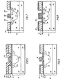
- Figures 1-10 are schematic views showing in cross-section a single cell of a MOSFET during different steps of the fabrication process in accordance with the present invention.
- Figure 11 is a schematic view in cross-section illustrating an IGT fabricated in accordance with the present invention.
- Figures 1-10 illustrate various steps in the fabrication of a single cell of a MOSFET.
- a wafer 10 is initially provided, preferably of silicon semiconductor material, comprising an N+ substrata 12 having an N epitaxial or wafer layer or drift region 14 thereon.
- N layer 14 includes a major surface 15 of the wafer.
- substrate 12 may comprise a commercially available silicon material doped with antimony to an impurity concentration level of about 10 19 atoms per cubic : 2 centimeter.
- N layer 14 may typically be epitaxially grown on substrate 12, and will have a thickness which will vary depending on the application for which the device is intended.
- N layer 14 has a phosphorous dopant concentration of about 10 15 atoms per cubic centimeter.
- a first insulating oxide layer 16 e.g. silicon dioxide
- major surface 15 preferably by thermal growth which results when wafer 10 is placed in a heated.furnace together with an oxidizing gas.
- Oxide layer 16 may also be formed by other processes, such as deposition on wafer 10. Further, other insulating layers may be used in lieu of oxide layer 16. In either case, layer 16 is deposited in a thickness of about 1,000 Angstroms.
- a gate electrode layer 18 (shown partially removed), comprising polysilicone or other refractory material, is next deposited on oxide layer 16. This may be suitably done using a process known as low pressure chemical vapor deposition (LPCVD). Layer 18 is deposited to a thickness of about 5,000 Angstroms.
- LPCVD low pressure chemical vapor deposition
- a first window 22 is opened in gate layer 18, preferably using photolithographic etching techniques. Oxide layer 16 remains in place.
- the shape of window 22 establishes the shape of the cell of the MOSFET being fabricated, e.g. a rectangular window 22 results in a rectangular cell.
- a protective oxide layer 20, having a thickness of about 500 Angstroms, is then formed on the exposed surfaces of gate electrode layer 18 and on oxide layer 16, preferably by thermal growth.
- a P-type dopant such as boron
- the dopant is driven in by heating to form.
- a first region 24 comprising a P base region.
- the depth of the implantation depends on the drive-in temperature, but may typically be between about 1.5 and 5 microns as measured from major surface 15.
- a first mask layer of silicon nitride (Si 3 N 4 ) 26 is next deposited on the MOSFET cell of Figure 2, preferably by LPCVD of a reaction product of silane (SiH 4 ) and ammonia (NH 3 ).
- a second window 28 is opened and is located centrally between the walls of window 22.
- Window 28 extends through silicon nitride layer 26 and oxide layers 20 and 16 to expose a portion of major surface 15.
- a suitable procedure to accomplish this is to first plasma etch away silicon nitride layer 26 in the area of window 28 and then to etch away the exposed portions of oxide layers 16 and 20 with a hydrofluoric acid (HF) based solution.
- HF hydrofluoric acid
- a layer of P-type dopant such as boron nitride, is deposited on the exposed portion of major surface 15 within window 18. This dopant is driven into water 10 by heating to form a second region 30 comprising a deep P+ base region.
- Region 30 has a predetermined depth between about 3-6 microns as measured from surface 15, depending on the desired device rating.
- the deep P+ base region By forming the deep P+ base region at this stage of fabrication, problems associated with the leaching out of the dopant by any overlying oxide layer are reduced. More specifically, the formation of the deep P + base region at a later stage in the fabrication process than is the case in the prior art results in less exposure of the region to the overlying oxide layers and therefore less of the dopant is leached out. As a consequence, final dopant concentration levels of greater than about 5 ⁇ 10 19 atoms per cubic centimeter are achievable in the fabrication process according to the present invention.
- a second mask layer in the form of an oxide layer 32 is formed on major surface 15 and completely fills window 28.
- the formation of layer 32 occurs preferably by thermal growth during the drive-in heating step for the formation of deep P+ base region 30.
- Oxide layer 32 must be thicker than oxide layer 16, for reasons that will become apparent below.
- silicon nitride layer 26 is subsequently removed, for example by placing wafer 10 in phosphoric acid heated to about 180°C. This procedure does not affect any of the oxide layers, i.e., layers 16, 20 and 32, which remain.
- oxide layer 20 and those portions of oxide layer 16 which do not underlie layer 18 are removed along with portions of oxide layer 32.
- This procedure is suitably accomplished by immersing wafer 10 in a hydrofluoric acid based solution for a predetermined time. Because of the greater thickness of layer 32, this immersion does not completely remove layer 32, but leaves behind a portion thereof to act as a mask for the introduction of the enitter region dopant.
- the last-described removal step opens a third window 34, which extends between the walls of window 22 ( Figure 2) and the regaining portion of oxide layer 32 centrally situated within window 22.
- An N-type dopant such as phosphorus or arsenic, is then introduced through window 34 into wafer 10.
- N+ source or emitter region 36 of shallow depth (e.g. 1 micron as measured from surface 15).
- Gate electrode layer 18 is concurrently doped.
- the resultant impurity concentration level in N+ source region 36 and in gate electrode layer 18 is about 5x10 19 atoms per cubic centimeter. It should be noted that gate electrode layer 18 may alternatively be doped at an earlier fabrication stage, or even during the formation of layer 18.
- a second insulating oxide layer 21 is next formed on the upper surface of gate electrode layer 18, as well as on the exposed portions of layers 16 and 18, of major surface 15 and of layer 32. This is preferably done by a combination of thermal oxidation and CVD.
- a photolithographic technique is used to open a fourth window 38, herein referred to as a contact window, through oxide layers 21 and 32.
- This procedure is suitably accomplished by immersing wafer 10 in a hydrofluoric acid-based solution for an interval sufficient to remove the oxide layers exposed by the contact window mask.
- Contact window 38 extends down to major surface 15 and exposes deep P+ base region 30 and a portion of N+ source region 36 at the latter surface.
- contact window 30 is narrower than window 22 by the thickness of layer 21 on the walls of the latter.
- the last-described removal step Leaves portions 23 of layer 21 on surface 15.
- a source metallization layer 40 is next applied to wafer 10, for example by evaporation of aluminum or an aluminum alloy.
- a collector metallization layer 42 may be deposited at this time on substrate 12 to complete the fabrication of MOSFET cell 44.
- source metallization layer 40 and collector metallization layer 42 are appropriately blased and a gate control voltage is applied to gate electrode 18 to induce a channel region 46 in base region 24 at major surface 15, between drift region 14 and source region 36, as shown in Figure 10.
- the flow of current through MOSFET cell 44 is thus controlled by variation of the gate control voltage.
- IGT 50 is similar in construction to MOSFET 44 ( Figure 10). However, while the latter includes a wafer 10 having N layer 14 on N+ substrate region 12, in IGT 50 a wafer 51 is provided having an N layer 52 on a P+ collector substrate 54. Accordingly, IGT 50 can be fabricated using substantially the same steps as are used in the fabrication of MOSFET 44, taking into account differences in substrate dopant type.
- the dopant concentrtion level in the deep base region is more precisely controllable as a result of reduced leaching of the dopant by the oxide layers during fabrication. Additionally, the electrical ruggedness of the overall device is improved by reducing sporadic breakdowns of the P-N junction during high voltage operation.
Landscapes
- Thyristors (AREA)
- Bipolar Transistors (AREA)
Applications Claiming Priority (2)
| Application Number | Priority Date | Filing Date | Title |
|---|---|---|---|
| US81770786A | 1986-01-10 | 1986-01-10 | |
| US817707 | 1986-01-10 |
Publications (3)
| Publication Number | Publication Date |
|---|---|
| EP0229362A2 true EP0229362A2 (de) | 1987-07-22 |
| EP0229362A3 EP0229362A3 (en) | 1989-08-30 |
| EP0229362B1 EP0229362B1 (de) | 1993-03-17 |
Family
ID=25223702
Family Applications (1)
| Application Number | Title | Priority Date | Filing Date |
|---|---|---|---|
| EP86117777A Expired - Lifetime EP0229362B1 (de) | 1986-01-10 | 1986-12-19 | Halbleitervorrichtung und Methode zur Herstellung |
Country Status (4)
| Country | Link |
|---|---|
| US (1) | US4810665A (de) |
| EP (1) | EP0229362B1 (de) |
| JP (1) | JP2551940B2 (de) |
| DE (1) | DE3688057T2 (de) |
Cited By (3)
| Publication number | Priority date | Publication date | Assignee | Title |
|---|---|---|---|---|
| NL8802032A (nl) * | 1987-08-19 | 1989-03-16 | Mitsubishi Electric Corp | Halfgeleider-element en werkwijze voor het vervaardigen ervan. |
| EP0435406A1 (de) * | 1989-12-29 | 1991-07-03 | STMicroelectronics S.r.l. | Verfahren zur Herstellung von Leistungsmos- und Halbleiteranordnungen und damit hergestellten Anordnungen |
| EP0410508A3 (en) * | 1989-07-24 | 1991-11-27 | Sgs-Thomson Microelectronics S.R.L. | Process for defining and forming an active region of very limited dimensions in a semiconductor layer |
Families Citing this family (21)
| Publication number | Priority date | Publication date | Assignee | Title |
|---|---|---|---|---|
| JPH01225164A (ja) * | 1988-03-03 | 1989-09-08 | Fuji Electric Co Ltd | 絶縁ゲートmosfetの製造方法 |
| JP2604777B2 (ja) * | 1988-01-18 | 1997-04-30 | 松下電工株式会社 | 二重拡散型電界効果半導体装置の製法 |
| JPH0734474B2 (ja) * | 1988-03-03 | 1995-04-12 | 富士電機株式会社 | 伝導度変調型mosfetの製造方法 |
| US5118638A (en) * | 1988-03-18 | 1992-06-02 | Fuji Electric Co., Ltd. | Method for manufacturing MOS type semiconductor devices |
| KR910004318B1 (ko) * | 1988-06-27 | 1991-06-25 | 현대전자산업 주식회사 | 수직형 d mos 트랜지스터의 셀 |
| JPH02163974A (ja) * | 1988-12-16 | 1990-06-25 | Mitsubishi Electric Corp | 絶縁ゲート型バイポーラトランジスタおよびその製造方法 |
| JPH02281662A (ja) * | 1989-04-21 | 1990-11-19 | Mitsubishi Electric Corp | 半導体装置 |
| US4931408A (en) * | 1989-10-13 | 1990-06-05 | Siliconix Incorporated | Method of fabricating a short-channel low voltage DMOS transistor |
| US5182222A (en) * | 1991-06-26 | 1993-01-26 | Texas Instruments Incorporated | Process for manufacturing a DMOS transistor |
| US5171705A (en) * | 1991-11-22 | 1992-12-15 | Supertex, Inc. | Self-aligned structure and process for DMOS transistor |
| US5284139A (en) * | 1991-12-30 | 1994-02-08 | Abbot Laboratories | Hemometrix temperature compensation |
| US5248627A (en) * | 1992-03-20 | 1993-09-28 | Siliconix Incorporated | Threshold adjustment in fabricating vertical dmos devices |
| US5426069A (en) * | 1992-04-09 | 1995-06-20 | Dalsa Inc. | Method for making silicon-germanium devices using germanium implantation |
| JP3297129B2 (ja) * | 1992-10-08 | 2002-07-02 | 株式会社東芝 | 半導体装置 |
| US5369045A (en) * | 1993-07-01 | 1994-11-29 | Texas Instruments Incorporated | Method for forming a self-aligned lateral DMOS transistor |
| EP0661755A1 (de) * | 1993-12-28 | 1995-07-05 | AT&T Corp. | Hochspannung-Halbleiteranordnung mit verbesserter elektrischer Robustheit und verminderter Zellschrittweite |
| KR0158608B1 (ko) * | 1993-12-29 | 1998-12-01 | 김광호 | 3단자 전력 절연 게이트 트랜지스터 및 그 제조방법 |
| US5422288A (en) * | 1994-05-19 | 1995-06-06 | Harris Corporation | Method of doping a JFET region in a MOS-gated semiconductor device |
| US5474946A (en) * | 1995-02-17 | 1995-12-12 | International Rectifier Corporation | Reduced mask process for manufacture of MOS gated devices |
| JP3279151B2 (ja) * | 1995-10-23 | 2002-04-30 | トヨタ自動車株式会社 | 半導体装置及びその製造方法 |
| US7736976B2 (en) * | 2001-10-04 | 2010-06-15 | Vishay General Semiconductor Llc | Method for fabricating a power semiconductor device having a voltage sustaining layer with a terraced trench facilitating formation of floating islands |
Family Cites Families (21)
| Publication number | Priority date | Publication date | Assignee | Title |
|---|---|---|---|---|
| JPS52132684A (en) * | 1976-04-29 | 1977-11-07 | Sony Corp | Insulating gate type field effect transistor |
| US4705759B1 (en) * | 1978-10-13 | 1995-02-14 | Int Rectifier Corp | High power mosfet with low on-resistance and high breakdown voltage |
| US4364073A (en) * | 1980-03-25 | 1982-12-14 | Rca Corporation | Power MOSFET with an anode region |
| US4345265A (en) * | 1980-04-14 | 1982-08-17 | Supertex, Inc. | MOS Power transistor with improved high-voltage capability |
| JPS5816571A (ja) * | 1981-07-23 | 1983-01-31 | Toshiba Corp | 半導体装置の製造方法 |
| DE3240162C2 (de) * | 1982-01-04 | 1996-08-01 | Gen Electric | Verfahren zum Herstellen eines doppelt-diffundierten Leistungs-MOSFET mit Source-Basis-Kurzschluß |
| IE55992B1 (en) * | 1982-04-05 | 1991-03-13 | Gen Electric | Insulated gate rectifier with improved current-carrying capability |
| US4503598A (en) * | 1982-05-20 | 1985-03-12 | Fairchild Camera & Instrument Corporation | Method of fabricating power MOSFET structure utilizing self-aligned diffusion and etching techniques |
| US4443931A (en) * | 1982-06-28 | 1984-04-24 | General Electric Company | Method of fabricating a semiconductor device with a base region having a deep portion |
| DE3224642A1 (de) * | 1982-07-01 | 1984-01-05 | Siemens AG, 1000 Berlin und 8000 München | Igfet mit injektorzone |
| US4417385A (en) * | 1982-08-09 | 1983-11-29 | General Electric Company | Processes for manufacturing insulated-gate semiconductor devices with integral shorts |
| US4466176A (en) * | 1982-08-09 | 1984-08-21 | General Electric Company | Process for manufacturing insulated-gate semiconductor devices with integral shorts |
| US4532534A (en) * | 1982-09-07 | 1985-07-30 | Rca Corporation | MOSFET with perimeter channel |
| JPS59125664A (ja) * | 1983-01-07 | 1984-07-20 | Toshiba Corp | 半導体装置の製造方法 |
| US4587713A (en) * | 1984-02-22 | 1986-05-13 | Rca Corporation | Method for making vertical MOSFET with reduced bipolar effects |
| JPS60196974A (ja) * | 1984-03-19 | 1985-10-05 | Toshiba Corp | 導電変調型mosfet |
| US4639762A (en) * | 1984-04-30 | 1987-01-27 | Rca Corporation | MOSFET with reduced bipolar effects |
| US4672407A (en) * | 1984-05-30 | 1987-06-09 | Kabushiki Kaisha Toshiba | Conductivity modulated MOSFET |
| US4631564A (en) * | 1984-10-23 | 1986-12-23 | Rca Corporation | Gate shield structure for power MOS device |
| US4641162A (en) * | 1985-12-11 | 1987-02-03 | General Electric Company | Current limited insulated gate device |
| JP2880004B2 (ja) * | 1991-08-15 | 1999-04-05 | 松下電器産業株式会社 | 車載用地図表示装置 |
-
1986
- 1986-12-19 DE DE86117777T patent/DE3688057T2/de not_active Expired - Fee Related
- 1986-12-19 EP EP86117777A patent/EP0229362B1/de not_active Expired - Lifetime
-
1987
- 1987-01-09 JP JP62001986A patent/JP2551940B2/ja not_active Expired - Lifetime
- 1987-07-24 US US07/077,711 patent/US4810665A/en not_active Expired - Lifetime
Cited By (6)
| Publication number | Priority date | Publication date | Assignee | Title |
|---|---|---|---|---|
| NL8802032A (nl) * | 1987-08-19 | 1989-03-16 | Mitsubishi Electric Corp | Halfgeleider-element en werkwijze voor het vervaardigen ervan. |
| US5047813A (en) * | 1987-08-19 | 1991-09-10 | Mitsubishi Denki Kabushiki Kaisha | Semiconductor device and method of manufacturing the same |
| US5468654A (en) * | 1987-08-19 | 1995-11-21 | Mitsubishi Denki Kabushiki Kaisha | Method of manufacturing an insulated gate bipolar transistor |
| EP0410508A3 (en) * | 1989-07-24 | 1991-11-27 | Sgs-Thomson Microelectronics S.R.L. | Process for defining and forming an active region of very limited dimensions in a semiconductor layer |
| EP0435406A1 (de) * | 1989-12-29 | 1991-07-03 | STMicroelectronics S.r.l. | Verfahren zur Herstellung von Leistungsmos- und Halbleiteranordnungen und damit hergestellten Anordnungen |
| US5141883A (en) * | 1989-12-29 | 1992-08-25 | Sgs-Thomson Microelectronics S.R.L. | Process for the manufacture of power-mos semiconductor devices |
Also Published As
| Publication number | Publication date |
|---|---|
| DE3688057T2 (de) | 1993-10-07 |
| US4810665A (en) | 1989-03-07 |
| EP0229362B1 (de) | 1993-03-17 |
| JPS62203380A (ja) | 1987-09-08 |
| JP2551940B2 (ja) | 1996-11-06 |
| EP0229362A3 (en) | 1989-08-30 |
| DE3688057D1 (de) | 1993-04-22 |
Similar Documents
| Publication | Publication Date | Title |
|---|---|---|
| US4810665A (en) | Semiconductor device and method of fabrication | |
| EP0139371B1 (de) | Verfahren zum Herstellen integrierter MOS-Schaltungen unter Verwendung eines Verfahrens zur Bildung von Oberflächenbereichen aus Siliciden hochschmelzender Metalle | |
| EP0034910B1 (de) | Verfahren zur Herstellung einer Halbleitervorrichtung und so hergestellte Vorrichtung | |
| EP0138978B1 (de) | Verfahren zum herstellen einer halbleiteranordnung mit kleinen abmessungen | |
| EP0227085B1 (de) | Verfahren zum Herstellen von IGFETs mit minimaler Übergangstiefe durch epitaktische Rekristallisation | |
| US4481706A (en) | Process for manufacturing integrated bi-polar transistors of very small dimensions | |
| JP2670563B2 (ja) | 半導体装置の製造方法 | |
| KR970000535B1 (ko) | Mos 전계효과 트랜지스터 및 그 회로 제조방법 | |
| EP0137645B1 (de) | Verfahren zur Bildung eines seichten Gebietes des N-Typs | |
| EP0221624A1 (de) | MOS-Transistor und Verfahren zur Herstellung | |
| US4486266A (en) | Integrated circuit method | |
| EP0132009A2 (de) | Verfahren zur Herstellung einer Halbleiteranordnung und nach diesem Verfahren hergestellte Halbleiteranordnung | |
| EP0033495B1 (de) | Verfahren zur Herstellung eines bipolaren Transistors mit hoher Geschwindigkeit | |
| US6429083B1 (en) | Removable spacer technology using ion implantation to augment etch rate differences of spacer materials | |
| US6445043B1 (en) | Isolated regions in an integrated circuit | |
| EP0023528A1 (de) | Doppelt diffundierte Transistor-Struktur und Verfahren zu deren Herstellung | |
| EP1032028B1 (de) | Verbessertes MOS-Halbleiterbauelement mit Graben | |
| JPS6133253B2 (de) | ||
| EP0104079A2 (de) | Kontaktstruktur für integrierte Schaltung | |
| RU1830156C (ru) | Способ изготовлени полупроводниковых приборов | |
| EP0042380B1 (de) | Verfahren zum erreichen eines idealen fremdstoffkonzentrationsverlaufs für die basiszone eines transistors | |
| GB1593694A (en) | Method for making a semiconductor device | |
| EP0193992B1 (de) | Verfahren zum Herstellen einer Feldeffektanordnung mit isoliertem Gate | |
| US20030062598A1 (en) | Method for manufacturing and structure of semiconductor device with sinker contact region | |
| US7164186B2 (en) | Structure of semiconductor device with sinker contact region |
Legal Events
| Date | Code | Title | Description |
|---|---|---|---|
| PUAI | Public reference made under article 153(3) epc to a published international application that has entered the european phase |
Free format text: ORIGINAL CODE: 0009012 |
|
| AK | Designated contracting states |
Kind code of ref document: A2 Designated state(s): DE NL |
|
| PUAL | Search report despatched |
Free format text: ORIGINAL CODE: 0009013 |
|
| AK | Designated contracting states |
Kind code of ref document: A3 Designated state(s): DE NL |
|
| 17P | Request for examination filed |
Effective date: 19900201 |
|
| 17Q | First examination report despatched |
Effective date: 19911023 |
|
| GRAA | (expected) grant |
Free format text: ORIGINAL CODE: 0009210 |
|
| AK | Designated contracting states |
Kind code of ref document: B1 Designated state(s): DE NL |
|
| REF | Corresponds to: |
Ref document number: 3688057 Country of ref document: DE Date of ref document: 19930422 |
|
| PLBE | No opposition filed within time limit |
Free format text: ORIGINAL CODE: 0009261 |
|
| STAA | Information on the status of an ep patent application or granted ep patent |
Free format text: STATUS: NO OPPOSITION FILED WITHIN TIME LIMIT |
|
| 26N | No opposition filed | ||
| NLS | Nl: assignments of ep-patents |
Owner name: HARRIS CORPORATION TE MELBOURNE, FLORIDA, VER. ST. |
|
| PGFP | Annual fee paid to national office [announced via postgrant information from national office to epo] |
Ref country code: NL Payment date: 19961120 Year of fee payment: 11 |
|
| PGFP | Annual fee paid to national office [announced via postgrant information from national office to epo] |
Ref country code: DE Payment date: 19961122 Year of fee payment: 11 |
|
| PG25 | Lapsed in a contracting state [announced via postgrant information from national office to epo] |
Ref country code: NL Free format text: LAPSE BECAUSE OF NON-PAYMENT OF DUE FEES Effective date: 19980701 |
|
| NLV4 | Nl: lapsed or anulled due to non-payment of the annual fee |
Effective date: 19980701 |
|
| PG25 | Lapsed in a contracting state [announced via postgrant information from national office to epo] |
Ref country code: DE Free format text: LAPSE BECAUSE OF NON-PAYMENT OF DUE FEES Effective date: 19980901 |