EP0237017A2 - Dispositif du type électrique ou électronique comportant une couche mince de polyimide - Google Patents
Dispositif du type électrique ou électronique comportant une couche mince de polyimide Download PDFInfo
- Publication number
- EP0237017A2 EP0237017A2 EP87103403A EP87103403A EP0237017A2 EP 0237017 A2 EP0237017 A2 EP 0237017A2 EP 87103403 A EP87103403 A EP 87103403A EP 87103403 A EP87103403 A EP 87103403A EP 0237017 A2 EP0237017 A2 EP 0237017A2
- Authority
- EP
- European Patent Office
- Prior art keywords
- group
- film
- thin film
- polyimide
- formula
- Prior art date
- Legal status (The legal status is an assumption and is not a legal conclusion. Google has not performed a legal analysis and makes no representation as to the accuracy of the status listed.)
- Granted
Links
- CIRJAMWSUJGNOV-UHFFFAOYSA-N CC(C(C=C1)C(OC=O)=O)C=C1Sc1cc(CC=C)cc(C(OC)=O)c1 Chemical compound CC(C(C=C1)C(OC=O)=O)C=C1Sc1cc(CC=C)cc(C(OC)=O)c1 CIRJAMWSUJGNOV-UHFFFAOYSA-N 0.000 description 1
- XTPALJOJDSYSGD-UHFFFAOYSA-N CC(C=CC12)=CC1C(O)OC2O Chemical compound CC(C=CC12)=CC1C(O)OC2O XTPALJOJDSYSGD-UHFFFAOYSA-N 0.000 description 1
- DZWDCVSFSVBJTK-UHFFFAOYSA-N CC1C=CC(CC(C(C=CC2C=C)=CC2C(OC)=O)=O)=CC1C(OC=O)=O Chemical compound CC1C=CC(CC(C(C=CC2C=C)=CC2C(OC)=O)=O)=CC1C(OC=O)=O DZWDCVSFSVBJTK-UHFFFAOYSA-N 0.000 description 1
- KTQMTIHIQJTEMU-UHFFFAOYSA-N O=C(C1C2C=CC(CS(=O)=O)C1)OC2=O Chemical compound O=C(C1C2C=CC(CS(=O)=O)C1)OC2=O KTQMTIHIQJTEMU-UHFFFAOYSA-N 0.000 description 1
Images






Classifications
-
- H—ELECTRICITY
- H10—SEMICONDUCTOR DEVICES; ELECTRIC SOLID-STATE DEVICES NOT OTHERWISE PROVIDED FOR
- H10P—GENERIC PROCESSES OR APPARATUS FOR THE MANUFACTURE OR TREATMENT OF DEVICES COVERED BY CLASS H10
- H10P14/00—Formation of materials, e.g. in the shape of layers or pillars
- H10P14/60—Formation of materials, e.g. in the shape of layers or pillars of insulating materials
- H10P14/68—Organic materials, e.g. photoresists
- H10P14/683—Organic materials, e.g. photoresists carbon-based polymeric organic materials, e.g. polyimides, poly cyclobutene or PVC
-
- G—PHYSICS
- G01—MEASURING; TESTING
- G01N—INVESTIGATING OR ANALYSING MATERIALS BY DETERMINING THEIR CHEMICAL OR PHYSICAL PROPERTIES
- G01N27/00—Investigating or analysing materials by the use of electric, electrochemical, or magnetic means
- G01N27/26—Investigating or analysing materials by the use of electric, electrochemical, or magnetic means by investigating electrochemical variables; by using electrolysis or electrophoresis
- G01N27/403—Cells and electrode assemblies
- G01N27/414—Ion-sensitive or chemical field-effect transistors, i.e. ISFETS or CHEMFETS
-
- H—ELECTRICITY
- H05—ELECTRIC TECHNIQUES NOT OTHERWISE PROVIDED FOR
- H05B—ELECTRIC HEATING; ELECTRIC LIGHT SOURCES NOT OTHERWISE PROVIDED FOR; CIRCUIT ARRANGEMENTS FOR ELECTRIC LIGHT SOURCES, IN GENERAL
- H05B33/00—Electroluminescent light sources
- H05B33/12—Light sources with substantially two-dimensional [2D] radiating surfaces
- H05B33/22—Light sources with substantially two-dimensional [2D] radiating surfaces characterised by the chemical or physical composition or the arrangement of auxiliary dielectric or reflective layers
-
- H—ELECTRICITY
- H10—SEMICONDUCTOR DEVICES; ELECTRIC SOLID-STATE DEVICES NOT OTHERWISE PROVIDED FOR
- H10D—INORGANIC ELECTRIC SEMICONDUCTOR DEVICES
- H10D1/00—Resistors, capacitors or inductors
- H10D1/60—Capacitors
- H10D1/62—Capacitors having potential barriers
- H10D1/66—Conductor-insulator-semiconductor capacitors, e.g. MOS capacitors
-
- H—ELECTRICITY
- H10—SEMICONDUCTOR DEVICES; ELECTRIC SOLID-STATE DEVICES NOT OTHERWISE PROVIDED FOR
- H10D—INORGANIC ELECTRIC SEMICONDUCTOR DEVICES
- H10D64/00—Electrodes of devices having potential barriers
- H10D64/01—Manufacture or treatment
- H10D64/013—Manufacture or treatment of electrodes having a conductor capacitively coupled to a semiconductor by an insulator
- H10D64/01302—Manufacture or treatment of electrodes having a conductor capacitively coupled to a semiconductor by an insulator the insulator being formed after the semiconductor body, the semiconductor being silicon
- H10D64/01332—Making the insulator
- H10D64/01336—Making the insulator on single crystalline silicon, e.g. chemical oxidation using a liquid
-
- H—ELECTRICITY
- H10—SEMICONDUCTOR DEVICES; ELECTRIC SOLID-STATE DEVICES NOT OTHERWISE PROVIDED FOR
- H10D—INORGANIC ELECTRIC SEMICONDUCTOR DEVICES
- H10D64/00—Electrodes of devices having potential barriers
- H10D64/60—Electrodes characterised by their materials
- H10D64/66—Electrodes having a conductor capacitively coupled to a semiconductor by an insulator, e.g. MIS electrodes
- H10D64/68—Electrodes having a conductor capacitively coupled to a semiconductor by an insulator, e.g. MIS electrodes characterised by the insulator, e.g. by the gate insulator
-
- H—ELECTRICITY
- H10—SEMICONDUCTOR DEVICES; ELECTRIC SOLID-STATE DEVICES NOT OTHERWISE PROVIDED FOR
- H10N—ELECTRIC SOLID-STATE DEVICES NOT OTHERWISE PROVIDED FOR
- H10N70/00—Solid-state devices having no potential barriers, and specially adapted for rectifying, amplifying, oscillating or switching
-
- H—ELECTRICITY
- H10—SEMICONDUCTOR DEVICES; ELECTRIC SOLID-STATE DEVICES NOT OTHERWISE PROVIDED FOR
- H10P—GENERIC PROCESSES OR APPARATUS FOR THE MANUFACTURE OR TREATMENT OF DEVICES COVERED BY CLASS H10
- H10P14/00—Formation of materials, e.g. in the shape of layers or pillars
- H10P14/60—Formation of materials, e.g. in the shape of layers or pillars of insulating materials
- H10P14/63—Formation of materials, e.g. in the shape of layers or pillars of insulating materials characterised by the formation processes
- H10P14/6326—Deposition processes
- H10P14/6342—Liquid deposition, e.g. spin-coating, sol-gel techniques or spray coating
- H10P14/6344—Liquid deposition, e.g. spin-coating, sol-gel techniques or spray coating using Langmuir-Blodgett techniques
-
- H—ELECTRICITY
- H10—SEMICONDUCTOR DEVICES; ELECTRIC SOLID-STATE DEVICES NOT OTHERWISE PROVIDED FOR
- H10P—GENERIC PROCESSES OR APPARATUS FOR THE MANUFACTURE OR TREATMENT OF DEVICES COVERED BY CLASS H10
- H10P14/00—Formation of materials, e.g. in the shape of layers or pillars
- H10P14/60—Formation of materials, e.g. in the shape of layers or pillars of insulating materials
- H10P14/63—Formation of materials, e.g. in the shape of layers or pillars of insulating materials characterised by the formation processes
- H10P14/6326—Deposition processes
- H10P14/6342—Liquid deposition, e.g. spin-coating, sol-gel techniques or spray coating
Definitions
- This invention relates to an electric-electronic device including heat resistant polyimide thin film excellent in electric insulation properties which is utilized in the field of electronics.
- LB film Langmuir-Blodgett film
- One object of this invention is to provide an electric-electronic device including a polyimide thin film excellent in heat resistance, mechanical strength, chemical resistance, and electrical insulating properties.
- the electric-electronic device can be produced by build-up of, for example, an amphiphilic polyimide precursor on a substrate, which may, if desired, have been processed beforehand, by the process of Langmuir-Blodgett (hereinafter referred to as LB process) followed by imidation to form a polyimide thin film and, if desired, processing the film afterwards.
- LB process Langmuir-Blodgett
- amphiphilic polyimide precursor which can be used suitably in the present invention has a repeating unit represented by formula (I) shown below and has a number average molecular weight ranging from 2,000 to 300,000, preferably 10,000 to 150,000.
- Formula (I) is represented by wherein R 1 is a tetravalent group having at least 2 carbon atoms, R 2 is a bivalent group having at least 2 carbon atoms, and R 3 , R 4 , R 5 and R 6 are hydrogen atom or a monovalent group having 1 to 30 carbon atoms selected from the group consisting of an aliphatic group, an alicyclic group, an aromatic group, a group in which an aliphatic group is combined with an aromatic group or an alicyclic group, and their groups substituted by a halogen atom, nitro group, amino group, cyano group, methoxy group or acetoxyl group, provided that at least one of R 3 , R 4 , R 5 and R 6 is not hydrogen atcm and the above-mentioned group which has 1 to 11 carbon atoms.
- the precursor has a tendency that the strength of the film prepared therefrom is too low, or that the viscosity of a solution thereof
- R 1 is a tetravalent group having at least two carbon atoms, preferably 5 to 20 carbon atoms. It may be an aromatic group; an alicyclic group; an aliphatic group; a group wherein an aromatic group and an aliphatic group are combined; a group wherein each of the above-mentioned groups is substituted by a monovalent group having 1 to 30 carbon atoms selected from the group consisting of an aliphatic group, an alicyclic group, an aromatic group, and a group in which an aliphatic group is combined with an alicyclic group or an aromatic group; or a group wherein each of the preceding groups is substituted by a monovalent group such as a halogen atom, nitro group, amino group, cyano group, methoxyl group or acetoxyl group, or by a group in which the above monovalent group bonds to -O-, -CCO-, -NHCO-, -CO-, -S-,
- R 1 Representative examples of R 1 are shown below.
- benzenoid as used herein means the same structure as a carbon ring contained in ordinary aromatic compounds, being used in comparison with “quinoid” as illustrated below.
- the positions in R 1 at which the four groups, are bonded are not particularly limited, but it is preferable that each pair of these groups are bonded to two adjacent carbon atoms constituting R 1 because such a polyimide precursor easily forms a 5-membered ring upon imidation.
- R 1 a group of is also preferred as R 1 .
- the group R in the formula (1) is a bivalent group having at least 2 carbon atoms. It may be an aromatic group; an aliphatic group; an alicyclic group; a group wherein an aromatic group and an aliphatic group are combined; a group wherein each of the above-mentioned bivalent groups is substituted by a monovalent group having 1 to 30 carbon atoms selected from the group consisting of an aliphatic group, an alicyclic group, an aromatic group and a group in which an aliphatic group is combined with an alicyclic group or an aromatic group; or a group wherein each of the preceding groups is substituted by a moncvalent group such as a halogen atom, nitro group, amino group, cyano group, methoxyl group or acetoxyl group, or by a group in which the above monovalent group bonds to -O-, -COO-, -NHCO-, -CO-, -S-, -CSS-, -NHCS-
- R 9 represents -(CH 2 ) m - (m represents an integer of from 1 to 3), in which R 10 and R 11 are an alkyl or aryl group having from 1 to 30 carbon atoms.
- R 9 is as defined above.
- Each of the groups R 3 , R 4 , R 5 and R 6 in the formula (1) is hydrogen atom or a monovalent group having 1 to 30 carbon atoms, preferably 1 to 22 carbon atoms, such as a monovalent aliphatic group, a monovalent alicyclic group, a monovalent aromatic group, a monovalent group wherein an aliphatic group is combined with an aromatic group or an alicyclic group, or their halogen, nitro, amino, cyano, methoxy or acetoxy substituted groups.
- R 3 , R 4 , R , and R are groups that are introduced to a polyamic acid unit represented by formula (VIII) shown below for the purpose of imparting hydrophobic properties to the polyamic acid unit to thereby obtain a stable condensed film.
- Formula (VIII) is represented by wherein R 1 and R 2 are as defined above.
- R 3 , R 4 , R 5 , and R 6 are the above-defined groups other than a hydrogen atom and those having from 1 to 11 carbon atoms, and preferably from 1 to 15 carbon atoms.
- R , R , R , and R 6 other than a hydrogen atom and those having from 1 to 11 carbon atoms are: wherein n represents an integer of from 12 to 30, and preferably from 16 to 22. In view of performance properties achieved and cost incurred, the most preterred among them are straight alkyl groups represented by CH 3 (CH2) ⁇ n-1 , wherein n is as defined above.
- R 3 , R 4 , R 5 , and R 6 e.g., a halogen atom, a nitro group, an amino group, a cyano group, a methoxy group, an acetoxy group, etc.
- groups containing a fluorine atom are preferred since presence of a fluorine atom in place of a hydrogen atom brings about a marked improvement on hydrophobic properties.
- R , R, and R are hydrogen atoms
- R , R, and R are hydrogen atoms
- Formula (II) is represented by wherein R 1 , R 2 , R 3 , and R 4 are as defined above, with proviso that R 3 and R 4 do not represent a hydrogen atom or a group having from 1 to 11 carbon atoms.
- Formula (III) is represented by wherein R 1 , R 2 , R 5 , and R are as defined above, with proviso that R 5 and R 6 do not represent a hydrogen atom or a group having from 1 to 11 carbon atoms.
- amphiphilic polyimide precursor having a recurring unit represented by formula (II) or (III) is preferred in view of ease in preparation and cost.
- amphiphilic polyimide precursor having the recurring unit represented by any of formulas (I), (II), and (III) are: wherein R 3 and R 4 specifically include CH 3 (CH 2 ) ⁇ 11 ' CH 3 (CH 2 ) ⁇ 13 , CH 3 (CH 2 ) ⁇ 15 , CH 3 (CH 2 ) ⁇ 17 , CH 3 (CH 2 ) 19 , CH 3 (CH 2 ) ⁇ 21 , CF 3 (CH 2 ) ⁇ 15 , etc.); and the arrow indicates isomerism (hereinafter the same); wherein R 5 and R 6 specifically include CH 3 (CH 2 ) ⁇ 11 , CH 3 (CH 2 ) ⁇ 13 , CH 3 (CH 2 ) ⁇ 15 , CH 3 (CH 2 ) ⁇ 17 , CH 3 (CH 2 ) ⁇ 19 , CH 3 (CH 2 ) ⁇ 21 , CF 3 (CH 2 ) ⁇ 15 , etc.; wherein R 3 and R 4 specifically include CH 3 (CH 2 ) ⁇ 11 , CH 3 (CH 2 ) ⁇
- the arrow indicating isomerism means that the respective formula includes two isomers.
- the formula includes isomers (a) and (b) as illustrated below.
- the respective formula for the amphiphilic polyimide precursor recurring unit may comprise either one of (a) and (b) alone or a combination of (a) and (b).
- amphiphilic polyimide precursors according to the present invention are easily soluble in organic polar solvents, such as N,N-dimethylacetamide, N,N-dimethylformamide, N,N-diethylformamide, hexamethylphosphoramide, and so on; soluble in a mixed solvent of such an organic polar solvent and an ordinary organic solvent, e.g., chloroform; and sparingly soluble or insoluble in ordinary organic solvents, such as benzene, ether, chloroform, acetone, methanol, etc.
- organic polar solvents such as N,N-dimethylacetamide, N,N-dimethylformamide, N,N-diethylformamide, hexamethylphosphoramide, and so on
- organic polar solvents such as N,N-dimethylacetamide, N,N-dimethylformamide, N,N-diethylformamide, hexamethylphosphoramide, and so on
- organic polar solvents
- amphiphilic polyimide precursors of the invention show infrared absorptions characteristic of an amido group, a carboxyl group or an ester thereof, and a long-chain alkyl group. They are also characterized by their thermal analysis showing a sudden weight loss starting at about 200°C and reaching a constant weight at about 400°C. After a constant weight is reached, absorptions characteristic of an amido group, a carboxyl group or an ester thereof, and a long-chain alkyl group disappear and, in turn, an absorption characteristic of an imide ring appears.
- Examples of these copolymers include those wherein at least one of R , R , R , R , and R 6 comprises at least two different groups selected from the representative examples recited for the respective group.
- the group to be replaced for a part of R is selected from groups containing at least two carbon atoms and having a valence other than 4, e.g., 2 or 3, and preferably 3.
- the copolymer is represented by either of the following formulas: wherein R 1 on the left side, R 2 , R 3 , R 4 , R 5 , and R 6 are as defined above; and R 1 on the right side represents a divalent (upper formula) or trivalent (lower formula) group containing at least two carbon atoms.
- the group to be replaced for a part of R 2 is selected from groups containing at least two carbon atoms and having a valence other than 2, and preferably a valence of 3 or 4.
- the copolymer is repressented by either of the following formulas: 1 2 3 4 5 6 wherein R 1 , R 2 on the left side, R 3 , R 4 , R 5 , and R 6 are as defined above; R 2 on the right side represents a trivalent (upper formula) or tetravalent (lower formula) group having at least two carbon atoms; and X represents a substituent on R , and preferably -NHR, -CONH 2 R, etc., wherein R represents an alkyl group or a hydrogen atom.
- Modification of the amphiphilic polyimide precursors by the above-mentioned copolymerization is important and preferable for improving ' build-up characteristics of the polyimide precursors in the LB process as well as physical properties of the polyimide thin film obtained by imidizing the precursor built - up on a substrate.
- R 9 is as defined above, wherein R 10 and R 11 each represents an alkyl or aryl group. wherein R 9 is as defined above, wherein R 9 is as defined above,
- amphiphilic polyimide precursor to be used may be copolymers containing a recurring unit represented by formula (IX) shown below in a proportion up to 30% by mole of the total recurring units.
- Formula (IX) is represented by whrein R 1 and R 2 are as defined above, R is a monovalent group having 1 to 11 carbon atoms selected from the group consisting of a monovalent aliphatic group, a monovalent alicyclic group, a monovalent aromatic group, a monovalent group in which an aliphatic group ⁇ is combined with an aromatic group or an alicyclic group, and their substituted monovalent groups with a halogen atom, nitro group, amino group, cyano group, methoxyl group or acetoxyl group, or hydrogen atom, and four groups R may be the same or different.
- the precursor having the recurring unit represented by formula (I) can be prepared by reacting a tetracarboxylic acid dianhydride represented by formula (IV) wherein R 1 is as defined above, with a compound represented by formula and a compound represented by formula wherein R 3 and R 4 are as defined above, to obtain a compound represented by formula (V) wherein R 1 , R 3 , and R are as defined above, converting the compound of formula (V) to an acid halide by treating with a halide, such as thionyl chloride, phosphorous pentachloride, benzenesulfonyl chloride, etc., in a substantially water-free polar solvent at a temperature not less than -10°C, and preferably about 0°C to about 40°C, and reacting the resulting acid halide with a compound represented by formula (VI) wherein R 2 , R 5 , and R are as defined above, at a temperature of from -10° to -20°C, and preferably from
- reaction temperature may be raised up to 20°C or higher after the addition of the compound of formula (IV).
- R 3 OH and R 4 OH are CH 3 0H, CH 3 C H 2 0H, CH 3 ( CH 2 ) 2 0H, CH 3 (CH 2 ) 3 OH, CH 3 (CH 2 ) 5 OH, CH 3 (CH 2 ) 7 OH, CH 3 (CH 2 ) 9 OH, CH 3 (CH 2 ) 11 OH, CH 3 (CH 2 ) 13 OH, CH 3 (CH 2 ) 15 OH, CH 3 (CH 2 ) 17 OH, CH 3 (CH 2 ) 19 OH, CH 3 ( CH 2 ) 21 0H, CH 3 (CH 2 ) 23 OH, CF 3 (CH 2 ) 15 OH, H(CH 2 ) 2 (CH 2 ) 15 OH, H(CF 2 ) 4 (CH 2 ) 13 OH, F(CF 2 ) 8 (CH 2 ) 2 OH, F(CF 2 ) 8 (CH 2 ) 4 OH, etc.
- reaction conditions for producing the compound (V) by the reaction of the tetracarboxylic acid dianhydride of formula (IV) with R 3 OH and R 4 OH are not particularly limited.
- the reaction can be carried out at about 100°C while stirring under a nitrogen stream for several hours, or under commonly employed conditions, such as stirring in a solvent, e.g., hexamethylphosphoramide, at room temperature for about 4 days.
- this reaction is carried out by heating at about 100°C for 3 hours under a nitrogen stream while stirring, and, after cooling, the reaction mixture is dissolved in hexamethylenephosphoramide and then subjected to the next reaction for converting into the acid halide.
- the polar solvent to be used in the conversion to an acid halide includes hexamethylenephosphoramide, N,N-dimethylacetamide, N,N-dimethylformamide, and the like. These solvents are used in a substantially water-free state so that the halide, such as thionyl chloride, phosphorus pentachloride, benzenesulfonyl chloride, etc., be not decomposed by moisture and the reaction proceed in the state nearly quantitatively.
- the reaction temperature is selected from the range of from -10°C to the vicinity of the boiling point of the produced acid halide.
- the thus prepared acid halide is then reacted with the compound (VI) to produce the precursor of the present invention.
- the thus prepared acid halide is subjected to the subsequent reaction as such without any isolation or purification procedure.
- reaction temperature ranges from -10° to 20°C, and preferably from 0° to 10°C. If the reaction temperature is lower than -10°C, the reaction system becomes heterogeneous due to freeze solidification and if it exceeds 20°C, unfavorable side reactions are apt to take place. In order to complete the reaction, the temperature may be raised up to 20°C or even higher after the addition of the compound of formula (VI).
- R 5 and R 6 specifically include CH 3 -, CH 3 CH 2 -, CH 3 (CH 2 ) ⁇ 2 , CH 3 (CH 2 ) ⁇ 3 , CH 3 (CH 2 ) ⁇ 5 , CH 3 (CH 2 ) ⁇ 11 , CH 3 (CH 2 ) ⁇ 13 , CH 3 (CH 2) ⁇ 15 , CH 3 (CH 2 ) 17 , CH 3 (CH 2 ) ⁇ 19 , CH 3 (CH 2 ) ⁇ 21 , CH 3 (CH 2 ) ⁇ 23 , CF 3 (CH 2 ) ⁇ 15 , H(CF 2 ) 2 (CH 2 ) ⁇ 15 , H(CF 2 ) 4 (CH 2 ) ⁇ 13 , F(CF 2 ) 8 (CH 2 ) ⁇ 2 , F(CF 2 ) 8 (CH 2 ) ⁇ 4 , etc.
- the ratio of the acid halide to the compound of formula (VI) is appropriately selected so as to produce the precursor having a desired molecular weight, and usually ranges from 1/0.8 to 1/1.2 by mole. In order to obtain the precursor having a high molecular weight, it is preferable to use stoichiometric amounts of purified monomers and purified solvents.
- both R 5 and R 6 in the compound of formula (VI) may be hydrogen atoms.
- the precursor having the recurring unit of formula (II) can be obtained.
- the precursor having the recurring unit of formula (I) wherein both R 4 and R 3 are hydrogen atoms i.e., the recurring unit represented by formula (III)
- the reaction between the tetracarboxylic acid dianhydride of formula (IV) and the compound of formula (VII) can be carried out under the conditions employed for the preparation of ordinary polyamic acids.
- the reaction is effected in a substantially water-free organic polar solvent at a temperature of not higher than 50°C, and preferably at room temperature.
- the compound of formula (VII) is used in an amount of from 0.8 to 1.2 mol per mol of the tetracarboxylic acid dianhydride of formula (IV).
- polyimide precursor having the recurring unit represented by formula (III) is characterized in that it is easily prepared as described above and that it can be formed in a film by the LB process, which is then heated to provide a polyimide film.
- copolymers can also be prepared in the same manner as described above for the amphiphilic polyimide precursors.
- LB films can be formed from the precursors of the present invention by any of the so-called LB technique without restriction, e.g., the vertical dipping method (LB method), the horizontal dipping method, the revolving cylindrical method and so on (as discrihed in Shin Jikken Kagaku Koza, Vol. 18, “Interface and Colloid", pages 498-508).
- the LB technique is a method in which a LB material is spread onto the surface of water and compressed at a constant surface pressure to form monomolecular layer film and the monomolecular layer is transferred onto a substrate.
- spreading of an LB film-forming substance on the surface of water is effected by using a solution of the substance in a solvent which is water-insoluble and is evaporated in a gaseous phase, such as benzene, chloroform, etc.
- a solvent which is water-insoluble and is evaporated in a gaseous phase such as benzene, chloroform, etc.
- an organic polar solvent is preferably used in combination in order to increase solubility of the precursor.
- Such an organic polar solvent includes N,N-dimethylformamide, N,N-dimethylacetamide, N,N-diethylformamide, N,N-diethylacetamide, N,N-dimethylmethoxyacetamide, dimethyl sulfoxide, N-methyl-2-pyrrolidone, pyridine, dimethylsulfone, hexa- methylphosphormaide, tetramethylenesulfone, dimethyl- tetramethylenesulfone, etc.
- the concentration of the precursor solution to be spread on the surface of water is not particularly limited, but usually ranges from about 2 to 5 x 10 -3 M. Addition of a metal ion to the solution or pH adjustment of the solution is not always required for obtaining satisfactory film-forming properties. Elimination of metal ions rather seems advantageous for use in the field of electronics.
- LB film-forming compounds which can be used in combination are well known in the art and described, e.g., in the above-cited references.
- the compounds of formula CH 3 (CH 2 ) n-1 Z are advantaegous in cost.
- those containing an unsaturated bond are polymerizable upon exposure to light or radiation.
- a mixing ratio of at least one of these LB film-forming compounds and the precursor of the invention is not particularly limited. Further, two or more compounds selected from the polyimide precursors and copolymers-according to the present invention may also be used as a mixture.
- the substrate on which LB films are formed is not particularly restricted and can be selected appropriately depending on the end use of the film. It should be noted, however, that the substrate is required to be heat resistant when the LB film thereon is heated for imidation.
- the substrate to be used examples include inorganic substrates made of glass, alumina, quartz, etc.; plastic substrates; inorganic or plastic plates on which a metal thin film is deposited; metal-made substrates; substrates of semi-conductors of the Groups VI, III-V, II-VI, etc. of the Periodic Table, e.g., Si, GaAs, ZnS, etc.; substrates made of good dielectrics, e.g., PtTiO 3 , BaTiO3, LiNbO3, LiTaO 3 , etc.; substrates made of ferromagnetic substances; and the like.
- the aforesaid metal thin film on the substrate may have a pattern suited for the particular applicaiton.
- the substrate made of a semi-conductor such as Si, GaAs, ZnS, etc. or a good dielectric may be processed beforehand to form elements. If desired, any of the above-enumerated substrates may be subjected to surface preparation commonly employed in the art.
- the polyimide precursors according to the present invention show a tendency of weak adhesion to glass, quartz, silicon, silicon dioxide, and the like, it is desirable to improve film-forming properties and adhesion by treating such a substrate with a silane coupling agent, and particularly a silane coupling agent having an amino group or an epoxy group and an alkoxy group, such as A-1100 or A-187 produced by UCC, or with a chelate containing aluminum to form an alumina layer. It is also possible, as is usual in the art, to form a few or several layers of a higher fatty acid metal salt on the substrace.
- a thin film excellent in heat resistance, mechanical characteristics, chemical resistance and electric insulation properties can be formed on a substrate according to the LB process. Imidation of the resulting film provides a thin film having further enhanced heat resistance.
- the process for imidation is not particularly limited, but imidation is generally carried out by heating at a temperature in the vicinity of 200 to 400°C.
- a laser beam may also be used for imidation. It may also be effected by the use of acetic anhydride or pyridine commonly employed for imidizing polyamic acids either alone or in combination with the thermal reaction.
- polyamic acid unit represented by formula (VIII) is also imidized to form a polyimide while forming H 2 0, such a polyimide cannot be utilized as an LB film.
- copolymers according to the present invention in which a part of R 1 and/or R 2 is replaced with a group having a different valence, also undergo reaction as illustrated below under the same conditions as described above.
- the last two of the above-illustrated reactions are advantageous in that a highly heat-resistant skeleton can be introduced to thereby assure heat resistance of the polyimide films.
- the imidation reaction or other cyclization reaction is accompanied by release of the groups having been introduced for rendering the precursor hydrophobic in the form of an alcohol. Since the thus released alcohol can be evaporated at a temperature in the vicinity of from 200° to 400°C, if desired, under a gas stream or in vacuo, a polyimide thin film having high heat resistance and excellent electric insulation properties can be obtained.
- the known LB film-forming compound to be added for improving film-forming properties can be selected from those which can be evaporated under the conditions for the imidation reaction or other cyclization reaction so as to obtain a polyimide thin film having high heat resistance and insulating properties.
- the polyimide thin film obtained by building up the amphiphilic polyimide precursor on a substrate by the LB process followed by imidation is excellent in heat resistance, mechanical characteristics, chemical resistance, and electric insulation properties.
- the polyimide thin film is very 0 thin as having a thickness of 10000 A or smaller, 0 0 e.g., 5000 A or 2000 A. If desired, it is possible to form a film having a thickness further reduced to 10 to 1000 A.
- the polyimide thin film exhibits satisfactory physical properties, inter alia, excellent insulating properties as having a dielectric breakdown strength of 1 x 10 6 V/cm or more, even with a 0 thickness of not more than 1000 A, e.g., several hundreds of angstroms or even smaller, e.g., about 50 to 100 A, it can be applied to a wide variety of electric-electronic devices.
- Thin films of from about 50 ⁇ to several hundreds of angstroms are particularly expected to exert specific effects ascribed to the small film thickness, such as a tunnel effect, and many interesting applications taking advantage of such an effect would be realized.
- MIS structure metal/insulating film/semi-conductor structure
- Figures 1 to 7 each illustrates a schematic view of a typical MIS structure.
- the structure of Fig. 1 comprises a semi-conductor substrate (S), an insulating film (I) formed by a polyimide thin film, and a metal electrode (M) in this order.
- the semi-conductors to be used include those of the Group IV of the Periodic Table, e.g., Si, Ge, etc.; those of the group III-V, e.g., GaAs, GaP, etc.; and those of the Group II-IV, e.g., CdTe, CdS, ZnS, ZnSe, CdHgTe, etc.
- the MIS structure using these semi-conductors can construct various semi-conductor devices, such as photoelectric elements, such as solar cells; emitter elements, such as light-emitting diodes (LED), EL, photodiodes, etc.; photoreceptor elements; light sensors; and various transducers, such as gas sensors, temperature sensors, etc.
- the semi-conductor to be used may have any of a single crystal form, a polycrystalline form, and an amorphous form.
- Fig. 2 also illustrates an MIS structure, in which two or more elements are formed on a substrate, which is of interest for application to charge-transport type devices, such as charge-coupled devices (CCD).
- CCD charge-coupled devices
- Fig. 3 illustrates a structure, in which an insulating substrate (IS) having an electrode (M), which may be a transparent electrode or may be patterned, has provided thereon a semi-conductor (S) in the form of, in many cases, a thin film, and further provided thereon a polyimide thin film (I) and an electrode (M) in this order.
- Fig. 4 is the same as Fig. 3 except that the polyimide thin film (I) is provided between the electrode (M) on the IS side and the semi-conductor film (S).
- the semi-conductor thin film can be prepared by any conventional processes, such as molecular beam epitaxy (MBE), metal organic compound vapor deposition (MOCVD), atomic layer epitaxy (ALE). vacuum evporation, sputtering, spray pyrolysis, coating, and the like.
- MBE molecular beam epitaxy
- MOCVD metal organic compound vapor deposition
- ALE atomic layer epitaxy
- the semi-conductor to be used in the structures of Figs. 3 and 4 can be selected from the same examples enumerated for the structures of Figs. 1 and 2, and the devices to which these structure are applicable are the same as for Figs. 1 and 2.
- MIS structure devices The most important structures of the MIS structure devices are so-called field effect transistor (FET) structures that are driven by controlling a channel current by gate electrodes as typically shown in Figs. 5 and 6.
- FET field effect transistor
- the structure of Fig. 5 uses a semi- conductor substrate (SS), while that of Fig. 6 uses an insulating substance (IS) on which a semi-conductor is formed usually in the form of a thin film.
- SS semi- conductor substrate
- IS insulating substance
- the MIS FET structure is one of basic device forms, by which various devices can be constructed.
- thin film transistors for driving liquid crystal displays can be obtained by constructing this structure on a substrate of a large area, and integrated circuits can be obtained by increasing the degree of integration.
- FIG. 5 and 6 Other interesting applications are structures of Figs. 5 and 6 from which the gate electrodes are removed.
- an insulating film either alone or in combination with a membrane sensitive to ions, gases or active substances to construct an ion-sensitive FET (ISFET), a gas-sensitive FET (Chem FET), an immune FET (IMFET), or an enzyme FET (ENFET).
- ISFET ion-sensitive FET
- Chem FET gas-sensitive FET
- IFET immune FET
- ENFET enzyme FET
- the operation principle can be accounted for by the field effect through the action of ions, gases or active substances upon the surface of the gate insulating film.
- the polyimide thin film of the present invention is advantageous as compared with the conventional inorganic substances when the thin film is further modified with various organic substances.
- Fig. 7 illustrates an example of ISFET, in which a silicon semi-conductor film is formed on a quartz substrate (IS) in such a manner as shown in the figure and an insulating film and an ion-sensitive film are provided thereon.
- the polyimide thin film according to the present invention can be used as the insulating film in this structure.
- the semi-conductors for constructing devices having an MIS structure are those of compounds of the Groups III-V, II-IV, etc. that are generally difficult to be formed in films having satisfactory insulating properties by oxidation or the like technique.
- the conventional devices using GaAs as a semi-conductor have been practically employed in the form of metal-semiconductor FET (MESFET) in the light of the above-described problem.
- MESFET metal-semiconductor FET
- an MIS integrated circuit When an MIS integrated circuit is constructed by using GaAs, an effect to decrease an operating voltage can be produced.
- an integral circuit operating at a high electron mobility (HEMT) taking advantage of high carrier mobility in the GaAs semiconductor can be produced through a very simple process.
- HEMT high electron mobility
- Figs. 8 to 10 each illustrates a schematic view of the MIM structure, in which a metal, an insulating film, and a metal are formed on an insulating substrate (IS) or a semi-conductor substrate (SS) in this order.
- IS insulating substrate
- SS semi-conductor substrate
- Fig. 8 illustrates a structure of a capacitor.
- the capacitor of this structure may also serve as a humidity sensor by tracing changes in capacitance with humidity.
- Transistors having an MIM structure can be produced in accordance with this structure.
- Fig. 9 illustrates an MIM structure when applied to a thermion transistor.
- Fig. 10 illustrates a strcuture applicable to a capacitor for a memory cell of VLSI, in which a capacitor is formed on a semi-conductor or a semi-conductor device. This structure is also applied to devices in which thermions are injected into a semi- conductor. Further, the metal can be replaced with an electromotive conductor, e.g., Nb, to produce a Josephson junction device (JJ).
- JJ Josephson junction device
- the devices of third importance containing the polyimide thin film of the present invention have an insulating film/metal structure (hereinafter referred to as IM structure) as schematically shown in Fig. 11.
- IM structure insulating film/metal structure
- This is the simplest structure obtained by forming a polyimide thin film as an insulating film on a metal layer.
- One of the applications is a liquid crystal oriented film, that is obtained by forming a polyimide film on a patterned electrode, usually a transparent electrode, e.g., ITO.
- Other applications are sensors for humidity, gases, etc. as shown in Figs. 12 and 13, wherein a polyimide film is formed on two independent electrodes.
- the thus obtained product was analyzed by IR spectrometry, thermogravimetric analysis (TGA) and differential thermal analysis (DTA), and its molecular weight was measured by the GP C method. The following results were obtained.
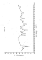
- the IR chart shown in Fig. 14 was obtained by the KBr disc method. Absorption peaks characteristic of esters, amides I, II and III, alkyl chains and ethers are observed in the chart.
- the thermal properties of the product were measured in a nitrogen stream by using an RTG-DTA of type (H) manufactured by Rigaku Densi Co., Ltd., under the following conditions: TGA full scale, 10 mg; DTA full scale, 100 uV; maximum temperature, 1,000°C, and rate of heating 10°C/min, and the results shown in Fig. 15 were obtained.
- TGA full scale
- DTA full scale
- 100 uV maximum temperature
- 1,000°C maximum temperature
- rate of heating 10°C/min and the results shown in Fig. 15 were obtained.
- TGA full scale
- DTA full scale 100 uV
- maximum temperature 1,000°C
- rate of heating 10°C/min and the results shown in Fig. 15 were obtained.
- TGA inflection points at 271, 318, 396 and 592°C.
- DTA is observed a characteristic peak at around 657°C.
- Fig. 16 shows TGA and DTA curves obtained at the time when a sample of the precursor was heated up to 400°C at a heating rate of 10°C/min, maintained at the same temperature for 1 hour, cooled to room temperature, and then heated again up to 1,000°C at a heating rate of 10°C/min.
- the sample When maintained at 400°C for 1 hour, the sample attained at almost constant weight, that is to say, the imidation reaction was completed.
- the sample was cooled to room temperature, and then reheated, it showed no change in its weight up to temperature exceeding 450°C, and its thermal decomposition started at 584°C, which is identical with the thermal decomposition temperature of corresponding commercial polyimide films. Accordingly, it can be said that a product having a heat resistance comparable to that of polyimide films could be obtained by completing the imidation.
- a number average molecular weight of ca. 50,000 (reduced to polystyrene) was obtained by GPC measured in N,N-dimethylformamide.
- the film was transferred onto a glass plate or a CaF 2 plate by Langmuir-Blodgett technique at a dipping speed of 10 mm/min, thereby maintaining the surface pressure at 25 dyne/cm.
- 90 Layers were deposited on the plate.
- a polyimide precursor was synthesized in the same manner as in Example 1, except that n-decyl alcohol (n-C 10 H 21 OH) was used instead of stearyl alcohol.
- n-decyl alcohol n-C 10 H 21 OH
- the polyimide precursor showed the same characteristics as those of the polyimide obtained in Example 1.
- the surface pressure-area curve of the precursor shown in Fig. 19, indicates the presence of a liquid expansion phase and denies the existence of a condensed phase. It would, therefore, be apparent that an alkyl group containing only 10 carbon atoms would be too short to give a polymer capable of forming a stable condensed film.
- Example 1 was repeated to synthesize a polyimide precursor, except that lauryl alcohol (containing 12 carbon atoms), myristyl alcohol (containing 14 carbon atoms) or cetyl alcohol (containing 16 carbon atoms) were used instead of stearyl alcohol.
- lauryl alcohol containing 12 carbon atoms
- myristyl alcohol containing 14 carbon atoms
- cetyl alcohol containing 16 carbon atoms
- a number average molecular weight of ca. 15,000 (reduced to polystyrene) was obtained by GPC measured in a mixed solvent of chloroform and N,N-dimethylacetamide (8:2).
- the deposition on the glass substrate on which aluminum was vacuum evaporated or which was treated with silane coupling agent A-1100 or A-187 was found to be of Y-type whether stearyl alcohol was added or not and the deposited film obtained was equally good.
- Example 6 The procedure of Example 6 was repeated to prepare a polyimide precursor, except for using stearic acid, w-heptadecenoic acid, or octadecane in place of stearyl alcohol.
- stearic acid w-heptadecenoic acid
- octadecane octadecane
- a built-up film composed of 11, 21, 31, 41, or 51 layers was produced in the same manner as in Example 2 except for using a 1:1 (molar ratio) mixture of the compound of Example 6 and stearyl alcohol.
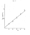
- the capacitance of the device was measured at a frequency of 1 kHz at room temperature and its reciprocal was plotted against the number of layers built up. The results are shown in Fig. 23. In Fig. 23, the bars indicate scatter of 10 data. The dissipation factor was about 0.02 in each case.
- a built-up film composed of 11, 21, 31, 41, 51, 101, or 151 layers was prepared in the same manner as above and heated at 400°C in a nitrogen stream for 1 hour.
- the resulting polyimide thin film had a thickness of about 50, 100, 150, 200, 250, 500, or 0 700 A, respectively.
- An aluminum/polyimide thin film/ aluminum device having a device area of 0.18 cm 2 was constructed using each of the built-up films.
- an electric field of 1 x 10 6 , 2 x 10 6 , 3 x 10 6 , 4 x 10 6 , or 5 x 10 6 V/cm was applied to ten samples each of these films, none of the samples underwent breakdown.
- the I (current) - V (voltage) characteristic of the device including the polyimide thin film of about 100 ⁇ in thickness is shown in Figs. 24 and 25.
- the device shows conduction properties that follow Ohm's law up to the voltage of 0.5 x 10 6 V/cm and thereafter follow 1nI ⁇ V1 ⁇ 2 Fig. 25 also proves that this film of about 100 A withstands an electric field of 10 V, i.e., 1 x 10 7 V/cm.
- the polyimide thin films in accordance with the present invention are suitable as insulating films in various electric-electronic devices.
- a ZnS(Mn) layer by electron beam vacuum evaporation using ZnS containing 0.7% by weight Mn as a target.
- the pressure for vacuum evaporation was about 1 x 10 -6 Torr; the substrate temperature was about 170°C; and the rate of film formation was about 10 A/sec.
- the resulting ZnS(Mn) thin layer was a polycrystalline film preferentially oriented to the direction of the face (111) and had a thickness of about 0.1 um.
- the resulting ZnS(Mn) layer was heat-treated at 600°C for 1 hour under a nitrogen stream.
- Example 9 A 1:1 (by mole) mixture of the compound of Example 6 and stearyl alcohol was deposited on the thus treated glass substrate under the same conditions as in Example 9 to build up 21 layers.
- the resulting build-up was of nearly ideal Y-type.
- the sample was heated at 400°C for 1 hour in a nitrogen stream to effect imidation reaction.
- An aluminum layer was then formed thereon by vacuum evaporation in the direction perpendicular to the ITO electrode to thereby obtain an EL device having an MIS structure.
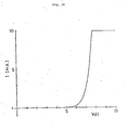
- Fig. 26 shows the plots of brightness vs. voltage for two of the devices when a direct voltage was applied to the ITO electrode positively and to the aluminum electrode negatively.
- the threshold voltage was 13 V
- the maximum brightness was 11 fL at 21 V with emission of a yellowish orange light.
- the device was heated at 150°C for 30 minutes, no change in initial performances was observed.
- a high brightness at a low voltage as above obtained is attributable to (1) injection of hot electrons into ZnS(Mn) due to an electric field of the insulating film, (2) an improved dielecrric breakdown strength of the device due to the pressure of the insulating film having high dielectric breakdown strength, (3) reduction in interfacial states between ZnS:Mn and aluminum, and the like.
- the example demonstrates that the polyimide thin film of the present invention effectively functions as an insulating film for devices having an MIS structure.
- the electric-electronic devices according to the present invention contain the polyimide thin film having a thickness not more ° than 1000 A and showing satisfactory insulating characteristics, the operating voltage can be reduced, and in particular, compound semi-conductors that find difficult in forming in good insulating films can be utilized in the devices effectively.
- polyimide thin film of the invention makes it possible to construct devices taking advantage of specific effects produced in the insulating film in a high electric field, such as hot electrons and a tunnel effect. Therefore, the present invention is extremely significant and beneficial in the industry.
Landscapes
- Life Sciences & Earth Sciences (AREA)
- Chemical & Material Sciences (AREA)
- Health & Medical Sciences (AREA)
- Physics & Mathematics (AREA)
- Biochemistry (AREA)
- Microelectronics & Electronic Packaging (AREA)
- Chemical Kinetics & Catalysis (AREA)
- Electrochemistry (AREA)
- Engineering & Computer Science (AREA)
- Analytical Chemistry (AREA)
- Molecular Biology (AREA)
- General Health & Medical Sciences (AREA)
- General Physics & Mathematics (AREA)
- Immunology (AREA)
- Pathology (AREA)
- Macromolecular Compounds Obtained By Forming Nitrogen-Containing Linkages In General (AREA)
- Formation Of Insulating Films (AREA)
- Polymers With Sulfur, Phosphorus Or Metals In The Main Chain (AREA)
- Investigating Or Analyzing Materials By The Use Of Electric Means (AREA)
Applications Claiming Priority (2)
| Application Number | Priority Date | Filing Date | Title |
|---|---|---|---|
| JP5408086 | 1986-03-11 | ||
| JP54080/86 | 1986-03-11 |
Publications (3)
| Publication Number | Publication Date |
|---|---|
| EP0237017A2 true EP0237017A2 (fr) | 1987-09-16 |
| EP0237017A3 EP0237017A3 (en) | 1990-03-28 |
| EP0237017B1 EP0237017B1 (fr) | 1995-09-06 |
Family
ID=12960632
Family Applications (1)
| Application Number | Title | Priority Date | Filing Date |
|---|---|---|---|
| EP87103403A Expired - Lifetime EP0237017B1 (fr) | 1986-03-11 | 1987-03-10 | Dispositif du type électrique ou électronique comportant une couche mince de polyimide |
Country Status (5)
| Country | Link |
|---|---|
| US (1) | US5072262A (fr) |
| EP (1) | EP0237017B1 (fr) |
| JP (2) | JPS63124A (fr) |
| CA (1) | CA1256591A (fr) |
| DE (1) | DE3751502T2 (fr) |
Cited By (3)
| Publication number | Priority date | Publication date | Assignee | Title |
|---|---|---|---|---|
| EP0239980A3 (fr) * | 1986-04-01 | 1990-04-11 | Kanegafuchi Kagaku Kogyo Kabushiki Kaisha | Dispositif électrique-électronique incluant une couche mince en polyimide |
| EP0247358A3 (fr) * | 1986-04-25 | 1990-09-12 | Kanegafuchi Kagaku Kogyo Kabushiki Kaisha | Précurseur de copolymère polyimide amphiphile, son procédé de préparation et film fin |
| EP0460435A3 (en) * | 1990-06-02 | 1993-02-24 | Basf Aktiengesellschaft | Reference electrode for chemical sensors |
Families Citing this family (34)
| Publication number | Priority date | Publication date | Assignee | Title |
|---|---|---|---|---|
| US4783395A (en) * | 1987-02-17 | 1988-11-08 | Hoechst Celanese Corporation | Desensitizing solution for lithographic printing plates |
| JPS6418760U (fr) * | 1987-07-25 | 1989-01-30 | ||
| JPH02140653A (ja) * | 1988-11-21 | 1990-05-30 | Kurabe:Kk | 湿度検知素子 |
| JP2814024B2 (ja) * | 1990-06-07 | 1998-10-22 | キヤノン株式会社 | 液晶素子 |
| US5329485A (en) * | 1990-11-01 | 1994-07-12 | Olympus Optical Co., Ltd. | Memory device |
| JPH05283542A (ja) * | 1992-03-31 | 1993-10-29 | Mitsubishi Electric Corp | 半導体集積回路装置及びその製造方法 |
| JP2709249B2 (ja) * | 1992-12-25 | 1998-02-04 | 川崎製鉄株式会社 | 圧延油供給装置 |
| US5408381A (en) * | 1994-04-28 | 1995-04-18 | Johnson Service Company | Capacitance humidity sensor |
| US5641974A (en) | 1995-06-06 | 1997-06-24 | Ois Optical Imaging Systems, Inc. | LCD with bus lines overlapped by pixel electrodes and photo-imageable insulating layer therebetween |
| DE19712233C2 (de) * | 1996-03-26 | 2003-12-11 | Lg Philips Lcd Co | Flüssigkristallanzeige und Herstellungsverfahren dafür |
| US6224787B1 (en) * | 1997-03-10 | 2001-05-01 | Dai Nippon Printing Co., Ltd. | Liquid crystalline charge transport material |
| JPH1173158A (ja) * | 1997-08-28 | 1999-03-16 | Seiko Epson Corp | 表示素子 |
| US6551399B1 (en) * | 2000-01-10 | 2003-04-22 | Genus Inc. | Fully integrated process for MIM capacitors using atomic layer deposition |
| TW507073B (en) * | 2000-03-31 | 2002-10-21 | Tdk Corp | Humidity sensor and method for making |
| JP2002243689A (ja) * | 2001-02-15 | 2002-08-28 | Denso Corp | 容量式湿度センサおよびその製造方法 |
| KR100428002B1 (ko) * | 2001-08-23 | 2004-04-30 | (주)그라쎌 | 유기 고분자 게이트 절연막을 구비하는 유기 반도체트랜지스터의 제조 방법 |
| US6962756B2 (en) * | 2001-11-02 | 2005-11-08 | Mitsubishi Gas Chemical Company, Inc. | Transparent electrically-conductive film and its use |
| EP1459392B1 (fr) * | 2001-12-19 | 2011-09-21 | Merck Patent GmbH | Transistor a effet de champ organique dote d'un dielectrique organique |
| TW544752B (en) * | 2002-05-20 | 2003-08-01 | Univ Nat Yunlin Sci & Tech | Method for producing SnO2 gate ion sensitive field effect transistor (ISFET), and method and device for measuring the temperature parameters, drift and hysteresis values thereof |
| US7228724B2 (en) * | 2002-10-17 | 2007-06-12 | Advanced Technology Materials, Inc. | Apparatus and process for sensing target gas species in semiconductor processing systems |
| US7080545B2 (en) * | 2002-10-17 | 2006-07-25 | Advanced Technology Materials, Inc. | Apparatus and process for sensing fluoro species in semiconductor processing systems |
| US7296458B2 (en) * | 2002-10-17 | 2007-11-20 | Advanced Technology Materials, Inc | Nickel-coated free-standing silicon carbide structure for sensing fluoro or halogen species in semiconductor processing systems, and processes of making and using same |
| US20060211253A1 (en) * | 2005-03-16 | 2006-09-21 | Ing-Shin Chen | Method and apparatus for monitoring plasma conditions in an etching plasma processing facility |
| TWI306882B (en) * | 2006-05-25 | 2009-03-01 | Ind Tech Res Inst | Thermoplastic polyimide composition and method of making double-sided flexible copper clad laminate using the same |
| JP2008072087A (ja) * | 2006-08-16 | 2008-03-27 | Kyoto Univ | 半導体装置および半導体装置の製造方法、ならびに表示装置 |
| JP4899033B2 (ja) * | 2007-04-04 | 2012-03-21 | 株式会社やまびこ | 送風作業機及び送風機のケーシング |
| CN101652656B (zh) * | 2007-04-05 | 2013-02-06 | 迈克纳斯公司 | 用于测量气态介质的湿度的湿度传感器和方法 |
| TWI410625B (zh) * | 2008-12-31 | 2013-10-01 | Ind Tech Res Inst | 氣體感測材料及包含其之氣體感測器 |
| US9134270B2 (en) * | 2010-03-25 | 2015-09-15 | Stichting Imec Nederland | Amorphous thin film for sensing |
| US8710615B2 (en) * | 2011-08-31 | 2014-04-29 | Infineon Technologies Ag | Semiconductor device with an amorphous semi-insulating layer, temperature sensor, and method of manufacturing a semiconductor device |
| WO2016125283A1 (fr) * | 2015-02-05 | 2016-08-11 | 富士通株式会社 | Capteur de gaz et dispositif de détection |
| CN107430086B (zh) * | 2015-03-10 | 2020-03-06 | 富士通株式会社 | 气体传感器以及传感器装置 |
| DE102016204308A1 (de) * | 2016-03-16 | 2017-09-21 | Continental Automotive Gmbh | Piezoelektrisches Aktuatorbauelement und Herstellungsverfahren zum Herstellen eines piezoelektrischen Aktuatorbauelementes |
| JP6770238B2 (ja) * | 2017-03-31 | 2020-10-14 | ミツミ電機株式会社 | 湿度センサ |
Citations (1)
| Publication number | Priority date | Publication date | Assignee | Title |
|---|---|---|---|---|
| JPS60157354A (ja) | 1984-01-26 | 1985-08-17 | Matsushita Electric Ind Co Ltd | 通信制御装置 |
Family Cites Families (10)
| Publication number | Priority date | Publication date | Assignee | Title |
|---|---|---|---|---|
| GB1572181A (en) * | 1975-08-18 | 1980-07-23 | Ici Ltd | Device comprising a thin film of organic materila |
| JPS5952822B2 (ja) * | 1978-04-14 | 1984-12-21 | 東レ株式会社 | 耐熱性感光材料 |
| JPS5839437B2 (ja) * | 1978-08-24 | 1983-08-30 | 岩崎通信機株式会社 | ボタン電話装置における本電話機接続方式 |
| JPS60197730A (ja) * | 1984-03-21 | 1985-10-07 | Ulvac Corp | ポリイミド膜の形成方法 |
| JPS60211836A (ja) * | 1984-04-06 | 1985-10-24 | Canon Inc | パタ−ン形成方法 |
| US4642665A (en) * | 1984-12-19 | 1987-02-10 | Eaton Corporation | Vertically layered MOMOM tunnel device |
| JPS62143929A (ja) * | 1985-07-16 | 1987-06-27 | Kanegafuchi Chem Ind Co Ltd | ポリイミド前駆体薄膜 |
| EP0239980A3 (fr) * | 1986-04-01 | 1990-04-11 | Kanegafuchi Kagaku Kogyo Kabushiki Kaisha | Dispositif électrique-électronique incluant une couche mince en polyimide |
| US4719281A (en) * | 1986-04-21 | 1988-01-12 | Hoechst Celanese Corporation | Pendant quinodimethane-containing polymer |
| CA1302675C (fr) * | 1986-05-20 | 1992-06-09 | Masakazu Uekita | Pellicule mince et dispositif pourvu de celle-ci |
-
1987
- 1987-03-10 DE DE3751502T patent/DE3751502T2/de not_active Expired - Fee Related
- 1987-03-10 EP EP87103403A patent/EP0237017B1/fr not_active Expired - Lifetime
- 1987-03-11 JP JP62056200A patent/JPS63124A/ja active Pending
- 1987-03-11 CA CA000531714A patent/CA1256591A/fr not_active Expired
- 1987-03-11 JP JP62056201A patent/JPH0693508B2/ja not_active Expired - Lifetime
-
1989
- 1989-10-10 US US07/418,618 patent/US5072262A/en not_active Expired - Fee Related
Patent Citations (1)
| Publication number | Priority date | Publication date | Assignee | Title |
|---|---|---|---|---|
| JPS60157354A (ja) | 1984-01-26 | 1985-08-17 | Matsushita Electric Ind Co Ltd | 通信制御装置 |
Non-Patent Citations (7)
| Title |
|---|
| "Interface and Colloid", SHIN JIKKEN KAGAKU KOZA, vol. 18, pages 498 - 508 |
| "Kagobutsu Handotai Device (I) & (II), Kogyo Chosakai" |
| "Kagobutsu Handotai Device", vol. I,II, 1984, KOGYO CHOSAKAI |
| E.S. YANG: "Fundamentals of Semiconductor Devices", 1978, MAGRAW-HILL |
| E.S. YANG: "Fundamentals of Semiconductor Devices", 1978, MCGRAW HILL |
| G.I. GAINS: "Insoluble Monolayers at Liquid-Gas Interfaces", 1966, INTERSCIENCE PUBLISHERS |
| P.S. VINCETT; G.G. ROBERTS, THIN SOLID FILMS, vol. 68, 1980, pages 135 - 171 |
Cited By (3)
| Publication number | Priority date | Publication date | Assignee | Title |
|---|---|---|---|---|
| EP0239980A3 (fr) * | 1986-04-01 | 1990-04-11 | Kanegafuchi Kagaku Kogyo Kabushiki Kaisha | Dispositif électrique-électronique incluant une couche mince en polyimide |
| EP0247358A3 (fr) * | 1986-04-25 | 1990-09-12 | Kanegafuchi Kagaku Kogyo Kabushiki Kaisha | Précurseur de copolymère polyimide amphiphile, son procédé de préparation et film fin |
| EP0460435A3 (en) * | 1990-06-02 | 1993-02-24 | Basf Aktiengesellschaft | Reference electrode for chemical sensors |
Also Published As
| Publication number | Publication date |
|---|---|
| EP0237017A3 (en) | 1990-03-28 |
| DE3751502T2 (de) | 1996-02-15 |
| DE3751502D1 (de) | 1995-10-12 |
| EP0237017B1 (fr) | 1995-09-06 |
| JPH0693508B2 (ja) | 1994-11-16 |
| JPS63124A (ja) | 1988-01-05 |
| CA1256591A (fr) | 1989-06-27 |
| US5072262A (en) | 1991-12-10 |
| JPS6312172A (ja) | 1988-01-19 |
Similar Documents
| Publication | Publication Date | Title |
|---|---|---|
| EP0237017B1 (fr) | Dispositif du type électrique ou électronique comportant une couche mince de polyimide | |
| EP0246602B1 (fr) | Dispositif comportant une couche mince en polymère | |
| US4897461A (en) | Amphiphilic polyimide precursor and process for preparing the same | |
| US5071733A (en) | Patterned thin film and process for preparing the same | |
| CA1290490C (fr) | Polymere amphiphile a chaines longues et procede pour sa production | |
| JPH05178679A (ja) | セラミック超電導体にポリイミド保護薄層を形成する方法 | |
| EP0218114B1 (fr) | Film et son procédé de fabrication | |
| US4987219A (en) | Copolymeric and amphiphilic polyimide precursor, process for preparing the same and thin film | |
| JPH0626704B2 (ja) | 基板との接着性が改良された超薄膜とその製法 | |
| EP0239980A2 (fr) | Dispositif électrique-électronique incluant une couche mince en polyimide | |
| Petty et al. | Pyroelectric Langmuir-Blodgett films prepared using preformed polymers | |
| US5171829A (en) | Copolymeric and amphiphilic polyimide precursor, process for preparing the same and thin film | |
| JPH0671575B2 (ja) | 薄 膜 | |
| JPS63126578A (ja) | 薄膜を含む複合物品 | |
| JPH058094B2 (fr) | ||
| JPH0259069A (ja) | パターン化された超薄膜の製法 | |
| CA1303281C (fr) | Couche mince a motif alterne, procede de fabrication | |
| JPS62232168A (ja) | 耐熱性ポリイミド薄膜を含む電気・電子デバイス | |
| EP0355810A2 (fr) | Procédé de structuration de films minces | |
| US4988570A (en) | Process for forming a film | |
| JPS62232169A (ja) | 3−v族化合物半導体デバイス | |
| JPS6349274A (ja) | ポリイミド前駆体薄膜を含む複合物品 | |
| JPS63218728A (ja) | 両性高分子化合物およびその製造法 | |
| JPH02232265A (ja) | パターン化された超薄膜の製法 | |
| JPH0236237A (ja) | パターン化された簿膜およびその製法 |
Legal Events
| Date | Code | Title | Description |
|---|---|---|---|
| PUAI | Public reference made under article 153(3) epc to a published international application that has entered the european phase |
Free format text: ORIGINAL CODE: 0009012 |
|
| AK | Designated contracting states |
Kind code of ref document: A2 Designated state(s): BE DE FR GB |
|
| PUAL | Search report despatched |
Free format text: ORIGINAL CODE: 0009013 |
|
| AK | Designated contracting states |
Kind code of ref document: A3 Designated state(s): BE DE FR GB |
|
| 17P | Request for examination filed |
Effective date: 19900601 |
|
| 17Q | First examination report despatched |
Effective date: 19920720 |
|
| GRAA | (expected) grant |
Free format text: ORIGINAL CODE: 0009210 |
|
| AK | Designated contracting states |
Kind code of ref document: B1 Designated state(s): BE DE FR GB |
|
| REF | Corresponds to: |
Ref document number: 3751502 Country of ref document: DE Date of ref document: 19951012 |
|
| ET | Fr: translation filed | ||
| PGFP | Annual fee paid to national office [announced via postgrant information from national office to epo] |
Ref country code: FR Payment date: 19951228 Year of fee payment: 10 |
|
| PGFP | Annual fee paid to national office [announced via postgrant information from national office to epo] |
Ref country code: GB Payment date: 19960301 Year of fee payment: 10 |
|
| PGFP | Annual fee paid to national office [announced via postgrant information from national office to epo] |
Ref country code: BE Payment date: 19960313 Year of fee payment: 10 |
|
| PGFP | Annual fee paid to national office [announced via postgrant information from national office to epo] |
Ref country code: DE Payment date: 19960530 Year of fee payment: 10 |
|
| PLBE | No opposition filed within time limit |
Free format text: ORIGINAL CODE: 0009261 |
|
| STAA | Information on the status of an ep patent application or granted ep patent |
Free format text: STATUS: NO OPPOSITION FILED WITHIN TIME LIMIT |
|
| 26N | No opposition filed | ||
| PG25 | Lapsed in a contracting state [announced via postgrant information from national office to epo] |
Ref country code: GB Effective date: 19970310 |
|
| PG25 | Lapsed in a contracting state [announced via postgrant information from national office to epo] |
Ref country code: BE Effective date: 19970331 |
|
| BERE | Be: lapsed |
Owner name: KANEGAFUCHI KAGAKU KOGYO K.K. Effective date: 19970331 |
|
| GBPC | Gb: european patent ceased through non-payment of renewal fee |
Effective date: 19970310 |
|
| PG25 | Lapsed in a contracting state [announced via postgrant information from national office to epo] |
Ref country code: FR Free format text: LAPSE BECAUSE OF NON-PAYMENT OF DUE FEES Effective date: 19971128 |
|
| PG25 | Lapsed in a contracting state [announced via postgrant information from national office to epo] |
Ref country code: DE Effective date: 19971202 |
|
| REG | Reference to a national code |
Ref country code: FR Ref legal event code: ST |