EP0238358A2 - Pufferschaltung - Google Patents
Pufferschaltung Download PDFInfo
- Publication number
- EP0238358A2 EP0238358A2 EP87302444A EP87302444A EP0238358A2 EP 0238358 A2 EP0238358 A2 EP 0238358A2 EP 87302444 A EP87302444 A EP 87302444A EP 87302444 A EP87302444 A EP 87302444A EP 0238358 A2 EP0238358 A2 EP 0238358A2
- Authority
- EP
- European Patent Office
- Prior art keywords
- transistors
- inverter
- transistor
- output
- delay
- Prior art date
- Legal status (The legal status is an assumption and is not a legal conclusion. Google has not performed a legal analysis and makes no representation as to the accuracy of the status listed.)
- Withdrawn
Links
Images


Classifications
-
- G—PHYSICS
- G11—INFORMATION STORAGE
- G11C—STATIC STORES
- G11C11/00—Digital stores characterised by the use of particular electric or magnetic storage elements; Storage elements therefor
- G11C11/21—Digital stores characterised by the use of particular electric or magnetic storage elements; Storage elements therefor using electric elements
- G11C11/34—Digital stores characterised by the use of particular electric or magnetic storage elements; Storage elements therefor using electric elements using semiconductor devices
- G11C11/40—Digital stores characterised by the use of particular electric or magnetic storage elements; Storage elements therefor using electric elements using semiconductor devices using transistors
-
- H—ELECTRICITY
- H03—ELECTRONIC CIRCUITRY
- H03K—PULSE TECHNIQUE
- H03K19/00—Logic circuits, i.e. having at least two inputs acting on one output; Inverting circuits
- H03K19/02—Logic circuits, i.e. having at least two inputs acting on one output; Inverting circuits using specified components
- H03K19/08—Logic circuits, i.e. having at least two inputs acting on one output; Inverting circuits using specified components using semiconductor devices
- H03K19/094—Logic circuits, i.e. having at least two inputs acting on one output; Inverting circuits using specified components using semiconductor devices using field-effect transistors
- H03K19/0944—Logic circuits, i.e. having at least two inputs acting on one output; Inverting circuits using specified components using semiconductor devices using field-effect transistors using MOSFET or insulated gate field-effect transistors, i.e. IGFET
- H03K19/0948—Logic circuits, i.e. having at least two inputs acting on one output; Inverting circuits using specified components using semiconductor devices using field-effect transistors using MOSFET or insulated gate field-effect transistors, i.e. IGFET using CMOS or complementary insulated gate field-effect transistors
-
- H—ELECTRICITY
- H03—ELECTRONIC CIRCUITRY
- H03K—PULSE TECHNIQUE
- H03K17/00—Electronic switching or gating, i.e. not by contact-making and –breaking
- H03K17/51—Electronic switching or gating, i.e. not by contact-making and –breaking characterised by the components used
- H03K17/56—Electronic switching or gating, i.e. not by contact-making and –breaking characterised by the components used by the use, as active elements, of semiconductor devices
- H03K17/687—Electronic switching or gating, i.e. not by contact-making and –breaking characterised by the components used by the use, as active elements, of semiconductor devices the devices being field-effect transistors
-
- H—ELECTRICITY
- H03—ELECTRONIC CIRCUITRY
- H03K—PULSE TECHNIQUE
- H03K19/00—Logic circuits, i.e. having at least two inputs acting on one output; Inverting circuits
- H03K19/0008—Arrangements for reducing power consumption
- H03K19/0013—Arrangements for reducing power consumption in field effect transistor circuits
-
- H—ELECTRICITY
- H03—ELECTRONIC CIRCUITRY
- H03K—PULSE TECHNIQUE
- H03K19/00—Logic circuits, i.e. having at least two inputs acting on one output; Inverting circuits
- H03K19/003—Modifications for increasing the reliability for protection
- H03K19/00346—Modifications for eliminating interference or parasitic voltages or currents
- H03K19/00361—Modifications for eliminating interference or parasitic voltages or currents in field effect transistor circuits
Definitions
- This invention relates to a buffer circuit.
- it relates to an output buffer circuit for a semiconductor integrated circuit.
- a conventional output circuit of a semiconductor integrated circuit device is constructed for example as shown in Fig. 1.
- reference numerals 11 to 14 represent CMOS inverters, constructed of P-channel MOS transistors Q1, Q3,,Q5 and Q7 and N - channel MOS transistors Q2, Q4, Q6 and Q8.
- a signal D1 from the internal circuitry (not shown) is fed to the gate of P-channel load MOS transistor Q9 through inverters 11 and 12 and to the gate of N-channel drive MOS transistor Q10 through inverters 13 and 14.
- These MOS transistors Q9 and Q10 are series-connected between power source Vcc and ground Vss. Output signal Dout is obtained from the point of connection of these transistors Q9 and Q10.
- Inverters 11 and 13 are arranged to prevent both MOS transistors Q9 and Q10 from being ON at the same time which would allow a DC through-current to pass from power source Vcc to ground Vss.
- the change of output from high ("H") level to low (“L") level for Inverter 11 takes place slightly before that of inverter 13, while the change of output from low ("L") level to high ("H") level for inverter 11 takes place slighly after that of inverter 13.
- This can be achieved for example by setting the dimension of MOS transistor Ql to be smaller than that of MOS transistor Q2, and by setting the dimension (gate length and/or width) of MOS transistor Q5 to be larger than that of MOS transistor Q6. This makes the threshold value of inverter 11 lower than that of inverters 12 and 14, and the threshold value of inverter 13 higher than that of inverters 12 and 14.
- Fig. 2(a) shows the waveforms of the various signals when signal D1 from the internal circuitry changes from “L” to “H” level
- Fig. 2(b) shows the waveforms of the various signals when signal D1 changes from "H” to "L” level.
- signal D1 from the internal circuitry begins to fall at time t1 from “H” level to “L” level.
- output D4 of inverter 13 starts to change from “L” level to “H” level
- output D2 of inverter 11 also starts to change from “L” level to “H” level.
- output D5 of inverter 14 begins to fall from “H “ level to “L” level. This turns drive MOS transistor Q10 OFF.
- drive MOS transistor Q10 is designed so as to permit a large current flow in order to satisfy the I OL specification. Consequently, when drive MOS transistor Q10 changes from the OFF state to the ON state, a large current flows, i.e. there is an abrupt increase in current consumption. This generates self-noise, which is a cause of spurious circuit operation.
- load MOS transistor Q9 is designed so as to permit a large current to flow in order to satisfy the I OH specification. Consequently, when load MOS transistor Q9 changes from the OFF state to the ON state, a large current flows, i.e. there is an abrupt increase in current consumption. This also generates self-noise, which is a cause of spurious circuit operation.
- the output buffer circuit of Fig. 1 has a drawback, since it is designed for a large current flow in order to satisfy the specification for I OH (high level output curreht)/I OL (1'ow level output current). This results in an abrupt increase of current consumption on inversion of the output, generating self-noise which is a cause of spurious circuit operation.
- the object of this invention is to remove this drawback and provide a buffer circuit wherein abrupt increase in current consumption can restrained and so generation of self-noise, causing spurious circuit operation, can be prevented.
- This invention provides a buffer circuit for a semiconductor integrated circuit having a power source voltage, an input node for receiving an input current from. the integrated circuit,, and an output node for outputting an output current responsive to the input current, comprising: load transistor means having first and second states, for increasing the input current of the buffer circuit from a first predetermined voltage when the load transistor means is in one of the first and second states; drive transistor means having first and second corresponding states, for increasing the input current of the buffer circuit from a second predetermined voltage when the load transistor means is in a state opposite to the one state; and means for reducing the rate of increase in the input current of the buffer circuit for stabilizing the power source voltage.
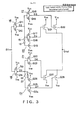
- signal D1 supplied from the internal circuitry is 'fed to a CMOS inverter 15 consisting of a P channel MOS transistor Q11 and an N channel MOS transistor Q12, and to a CMOS inverter 16 consisting of a P channel MOS transistor Q13 and an N channel MOS transistor Q14.
- the output D2 of this inverter 15 is fed to a CMOS inverter 17 consisting of a P channel M O S transistor Q15 and an N channel MOS transistor Q16.
- This output D2 is also supplied to the gate of a P channel MOS transistor Q17, one end of which is connected to power source Vcc, and to the gate of an N channel MOS transistor Q18, one end of which is connected to the other end of this MOS transistor Q17.
- the output of this inverter 15 is fed through delay elements such as inverters 18 and 19 to the gate of an N channel MOS transistor Q19 that is connected between the other end of this MOS transistor Q18 and ground node Vss.
- These MOS transistors Q17, Q18 and Q19 act as delay means such as an inverter 20 that has a delay action only when the output level is "L".
- inverter 17 is supplied to the gate of a P channel load MOS transistor Q20, one end of which is connected to power source Vcc.
- the output of inverter 20 is delivered from the point of connection of these MOS transistors Q17 and Q18, and supplied to the gate of P-channel load MOS transistor Q21.
- One end of transistor Q21 is connected to power source Vcc.
- the other ends of MOS transistors Q20 and Q21 are connected in common.
- inverter 16 is fed to a CMOS inverter 21 consisting of a P channel MOS transistor Q22 and an N channel MOS transistor Q23. This output also is supplied to the gate of an N channel MOS transistor Q24, one end of which is connected to ground node Vss. The output also is supplied to the gate of a P channel MOS transistor Q25, one end of which is connected to the other end of this MOS transistor Q24. The output of inverter 16 also is fed through delay elements such as inverters 22 and 23 to the gate of a P channel MOS transistor Q26 that is connected between the other end of this MOS transistor Q25 and power source Vcc. These MOS transistors Q24, Q25 and Q 26 act as delay means such as an inverter 24.
- the output of inverter 21 is supplied to the gate of an N channel drive MOS transistor Q27 that is connected between the common connection point of the other ends of MOS transistors Q20 and Q21 and ground node Vss.
- the output of inverter 24 that is delivered from the point of connection of these MOS transistors Q24 and Q25 is supplied to the gate of an N channel drive MOS transistor Q28.
- Transistor Q28 is connected between the point of common connection of the other ends of MOS transistors Q20 and Q21 and ground node Vss.
- the total current capacity of transistors Q27 and Q28 is equal to the current capacity of transistor Q10 in the prior art. A similar condition applied to transistors Q27 and Q28, compared with Q10.
- Fig. 4(a) shows the waveforms of the various signals when signal Dl.from the in internal circuitry changes from "L" level to "H” level.
- Fig. 4 (b) shows a comparison of the output current waveforms that are then obtained with the conventional circuit and with the circuit of this embodiment.
- Fig. 5(a) shows the waveforms of the various signals when signal Dl from the internal circuitry changes from "H" level to "L” level.
- Fig. 5(b) shows a comparison of the output current waveforms that are then obtained with the conventional circuit and with the circuit of this embodiment.
- drive MOS transistor Q27 is turned ON (at time-point t5) by the output of inverter 21, and drive MOS transistor Q28 is turned ON at time-point t7. Consequently at time-point t5 output signal Dout starts to fall slowly from "H” level to "L” level, becoming “L” level at time-point t8 after a prescribed time has lapsed since time-point t7. Thus the current between time-point t5 and t8 at which this output signal Dout is inverted follows a gentle gradient as shown in Fig. 4(b), with no abrupt increase in current.
- load MOS transistors Q20 and Q21 are turned ON sequentially with a prescribed time interval, and drive MOS transistors Q27 and Q28 are turned ON sequentially with a prescribed time interval.
- the noise margin of the semiconductor integrated circuit device can therefore be increased.
- load MOS transistors Q20 and Q21 or drive MOS transistors Q27 and Q28 change simultaneously from the ON state to the OFF state, there can be no great loss of speed of operation.
- load MOS transistors Q20 and Q21 and drive MOS transistors Q27 and Q28 going simultaneously ON, there is no possibility of D.C. through-current.
- Fig. 6 is a circuit diagram of a buffer circuit according to another embodiment of this invention. As shown in Fig. 6, it differs from the embodiment described above with reference to Fig. 3 in that a delay element is constituted by resistors 60 and 64 and capacitors 62 and 66. The same symbols as appears in Fig. 3 are used for the other components shown in Fig. 6.
- Fig. 7 is a circuit diagram of a buffer circuit according to another embodiment of this invention. As shown in Fig. 7, it differs from the embodiment described above with reference to Fig. 3 in that a delay element is constituted by a depletion type MOS transistors Q70 to Q73 whose gate and source are connected to each other. The same symbols as appears in Fig. 3 are used for the other components shown in Fig. 7.
- Fig. 8 is a circuit diagram of a buffer circuit according to another embodiment of this invention. This circuit is constituted by three load MOS transistors and three drive transistors. As shown in Fig. 8, it differs from the embodiment described above with reference to Fig. 3 in that a delay means such as inverters 80 and 86, a load transistor Q80, and a drive transistor Q82 are added to the buffer circuit shown in Fig. 3. The same symbols as appears in Fig. 3 are used for the other components shown in Fig. 8.
- An output D8 of inverters 18 and 19 is supplied to the delay means such as inverter 80.
- the construction of this inverter 80 is same as that of inverter 20.
- MOS transistors Q84, Q85 and Q86 act as the inverter that has a delay action only when the output Dout level is "L".
- the output of inverter 80 is delivered from the point of connection of these MOS transistors Q84 and Q85, and supplied to the gate of P-channel load MOS transistor Q80.
- One end of transistor Q80 is connected to power source Vcc.
- the other end of MOS transistors Q20, Q21 and Q80 are connected in common.
- An output D10 of inverters 22 and - 23 is supplied to the delay means such as an inverter 86.
- the construction of this inverter 86 is same as that of inverter 24.
- MOS transistors Q87, Q88 and Q89 act as the inverter that has a delay action only when the output Dout level is "H".
- the output of inverter 86 is delivered from the point of connection of these MOS transistors Q87 and Q88, and supplied to the gate of N-channel drive MOS transistor Q82.
- One end of transistor Q82 is connected to power source Vss.
- the other end of MOS transistors Q27, Q28 and Q82 are connected in common.
- Output signal Dout shown in Fig. 8 follows a gentler gradient compared with the embodiment of Fig. 3 with no abrupt increase in current.
- a buffer circuit can be obtained wherein abrupt increase in current consumption is avoided and the generation of self-noise, which is a cause of spurious circuit operation, is thereby prevented.
Landscapes
- Engineering & Computer Science (AREA)
- Computer Hardware Design (AREA)
- Physics & Mathematics (AREA)
- Computing Systems (AREA)
- General Engineering & Computer Science (AREA)
- Mathematical Physics (AREA)
- Power Engineering (AREA)
- Microelectronics & Electronic Packaging (AREA)
- Logic Circuits (AREA)
- Electronic Switches (AREA)
Applications Claiming Priority (2)
| Application Number | Priority Date | Filing Date | Title |
|---|---|---|---|
| JP63214/86 | 1986-03-20 | ||
| JP61063214A JPS62220026A (ja) | 1986-03-20 | 1986-03-20 | 出力バツフア回路 |
Publications (2)
| Publication Number | Publication Date |
|---|---|
| EP0238358A2 true EP0238358A2 (de) | 1987-09-23 |
| EP0238358A3 EP0238358A3 (de) | 1989-10-18 |
Family
ID=13222722
Family Applications (1)
| Application Number | Title | Priority Date | Filing Date |
|---|---|---|---|
| EP87302444A Withdrawn EP0238358A3 (de) | 1986-03-20 | 1987-03-20 | Pufferschaltung |
Country Status (4)
| Country | Link |
|---|---|
| US (1) | US4785203A (de) |
| EP (1) | EP0238358A3 (de) |
| JP (1) | JPS62220026A (de) |
| KR (1) | KR900004590B1 (de) |
Cited By (7)
| Publication number | Priority date | Publication date | Assignee | Title |
|---|---|---|---|---|
| EP0351820A3 (en) * | 1988-07-19 | 1990-05-30 | Kabushiki Kaisha Toshiba | Output circuit |
| EP0329285A3 (en) * | 1988-02-11 | 1990-09-19 | Advanced Micro Devices, Inc. | Output buffer |
| EP0301603A3 (de) * | 1987-07-31 | 1991-04-03 | Kabushiki Kaisha Toshiba | Ausgangsschaltung einer integrierten Halbleiterschaltungsanordnung |
| EP0414354B1 (de) * | 1989-06-28 | 1994-04-13 | Digital Equipment Corporation | CMOS-Ausgangskupplungsanordnung für Niederspannung |
| EP0913927A1 (de) * | 1997-10-31 | 1999-05-06 | STMicroelectronics S.r.l. | Hochspannungspegelverschieber zum Steuern einer Ausgangsstufe |
| US6288660B1 (en) | 1998-03-18 | 2001-09-11 | Telefonaktiebolaget Lm Ericsson | BiCMOS circuit for controlling a bipolar current source |
| CN103236834A (zh) * | 2013-03-13 | 2013-08-07 | 东南大学 | 浮栅驱动芯片中抑制高侧浮动电源低电平负过冲的电路 |
Families Citing this family (49)
| Publication number | Priority date | Publication date | Assignee | Title |
|---|---|---|---|---|
| JPS63234622A (ja) * | 1987-03-23 | 1988-09-29 | Toshiba Corp | デ−タ出力回路 |
| JPS63299513A (ja) * | 1987-05-29 | 1988-12-07 | Toshiba Corp | 出力回路 |
| US5268868A (en) * | 1987-09-16 | 1993-12-07 | Hitachi, Ltd. | Output buffer circuits for reducing ground bounce noise |
| JPH01161916A (ja) * | 1987-12-18 | 1989-06-26 | Toshiba Corp | 半導体集積回路 |
| JPH01171320A (ja) * | 1987-12-25 | 1989-07-06 | Nec Ic Microcomput Syst Ltd | 出力回路 |
| NL8800234A (nl) * | 1988-02-01 | 1989-09-01 | Philips Nv | Geintegreerde schakeling met logische circuits en ten minste een push-pull-trap. |
| US4877980A (en) * | 1988-03-10 | 1989-10-31 | Advanced Micro Devices, Inc. | Time variant drive circuit for high speed bus driver to limit oscillations or ringing on a bus |
| US4992677A (en) * | 1988-03-23 | 1991-02-12 | Hitachi, Ltd. | High speed MOSFET output buffer with low noise |
| JP2666347B2 (ja) * | 1988-04-20 | 1997-10-22 | セイコーエプソン株式会社 | 出力回路 |
| JP2542678B2 (ja) * | 1988-06-17 | 1996-10-09 | 富士通株式会社 | 半導体装置 |
| US5293082A (en) * | 1988-06-21 | 1994-03-08 | Western Digital Corporation | Output driver for reducing transient noise in integrated circuits |
| US4959563A (en) * | 1988-06-29 | 1990-09-25 | Texas Instruments Incorporated | Adjustable low noise output circuit |
| US4924120A (en) * | 1988-06-29 | 1990-05-08 | Texas Instruments Incorporated | Low noise output circuit |
| JPH0289292A (ja) * | 1988-09-26 | 1990-03-29 | Toshiba Corp | 半導体メモリ |
| JPH0289373A (ja) * | 1988-09-27 | 1990-03-29 | Nec Corp | 半導体メモリ |
| US5136179A (en) * | 1988-10-31 | 1992-08-04 | Teledyne Industries, Inc. | Logic level discriminator |
| JPH0777345B2 (ja) * | 1988-11-04 | 1995-08-16 | 三菱電機株式会社 | 半導体装置 |
| JPH0666674B2 (ja) * | 1988-11-21 | 1994-08-24 | 株式会社東芝 | 半導体集積回路の出力回路 |
| US5063308A (en) * | 1988-12-21 | 1991-11-05 | Intel Corporation | Output driver with static and transient parts |
| US4975598A (en) * | 1988-12-21 | 1990-12-04 | Intel Corporation | Temperature, voltage, and process compensated output driver |
| US4933574A (en) * | 1989-01-30 | 1990-06-12 | Integrated Device Technology, Inc. | BiCMOS output driver |
| US5004936A (en) * | 1989-03-31 | 1991-04-02 | Texas Instruments Incorporated | Non-loading output driver circuit |
| US4992676A (en) * | 1989-05-01 | 1991-02-12 | Motorola, Inc. | Output buffer having distributed stages to reduce switching noise |
| US4972101A (en) * | 1989-09-19 | 1990-11-20 | Digital Equipment Corporation | Noise reduction in CMOS driver using capacitor discharge to generate a control voltage |
| US4962345A (en) * | 1989-11-06 | 1990-10-09 | Ncr Corporation | Current limiting output driver |
| JP3031419B2 (ja) * | 1990-06-13 | 2000-04-10 | 三菱電機株式会社 | 半導体集積回路 |
| US5097149A (en) * | 1990-07-02 | 1992-03-17 | Micron Technology, Inc. | Two stage push-pull output buffer circuit with control logic feedback for reducing crossing current, switching noise and the like |
| US5241221A (en) * | 1990-07-06 | 1993-08-31 | North American Philips Corp., Signetics Div. | CMOS driver circuit having reduced switching noise |
| US5041741A (en) * | 1990-09-14 | 1991-08-20 | Ncr Corporation | Transient immune input buffer |
| US5122690A (en) * | 1990-10-16 | 1992-06-16 | General Electric Company | Interface circuits including driver circuits with switching noise reduction |
| JPH04153761A (ja) * | 1990-10-17 | 1992-05-27 | Nec Corp | 出力バッファ |
| JP2583684B2 (ja) * | 1990-11-06 | 1997-02-19 | 三菱電機株式会社 | プルダウン抵抗コントロール入力回路及び出力回路 |
| JP2628942B2 (ja) * | 1990-11-06 | 1997-07-09 | 三菱電機株式会社 | プルアップ抵抗コントロール入力回路及び出力回路 |
| JPH05243940A (ja) * | 1992-02-27 | 1993-09-21 | Mitsubishi Electric Corp | 出力バッファ装置 |
| JP3442149B2 (ja) * | 1994-07-28 | 2003-09-02 | 富士通株式会社 | 半導体回路 |
| US5701090A (en) * | 1994-11-15 | 1997-12-23 | Mitsubishi Denki Kabushiki Kaisha | Data output circuit with reduced output noise |
| KR100219559B1 (ko) * | 1996-10-09 | 1999-09-01 | 윤종용 | 신호라인 구동회로 및 이를 구비하는 반도체장치 |
| US5910730A (en) * | 1996-12-13 | 1999-06-08 | International Business Machines Corporation | Digital circuit noise margin improvement |
| US5825219A (en) * | 1997-02-21 | 1998-10-20 | Silicon Integrated System Corp. | Fast edge rate signal driver |
| US5929680A (en) * | 1997-05-16 | 1999-07-27 | Tritech Microelectronics International Ltd | Short circuit reduced CMOS buffer circuit |
| US6051995A (en) * | 1998-09-11 | 2000-04-18 | Sharp Electronics Corporation | Constant impedance, low noise CMOS buffer |
| US6466074B2 (en) * | 2001-03-30 | 2002-10-15 | Intel Corporation | Low skew minimized clock splitter |
| US6683482B2 (en) * | 2001-08-02 | 2004-01-27 | Agilent Technologies, Inc. | Slew rate control of output drivers using PVT controlled edge rates and delays |
| US6529050B1 (en) * | 2001-08-20 | 2003-03-04 | National Semiconductor Corporation | High-speed clock buffer that has a substantially reduced crowbar current |
| US6870895B2 (en) * | 2002-12-19 | 2005-03-22 | Semiconductor Energy Laboratory Co., Ltd. | Shift register and driving method thereof |
| US20040246039A1 (en) * | 2003-06-03 | 2004-12-09 | Chi-Ming Hsiao | Switched capacitor circuit capable of minimizing clock feedthrough effect in a voltage controlled oscillator circuit |
| TWI262315B (en) * | 2004-11-17 | 2006-09-21 | Richtek Technology Corp | Detecting method of switching state for a FET-based switch |
| WO2006064822A1 (en) * | 2004-12-13 | 2006-06-22 | Semiconductor Energy Laboratory Co., Ltd. | Semiconductor device and electronic appliance using the same |
| US11349456B2 (en) | 2017-07-21 | 2022-05-31 | Texas Instruments Incorporated | Ultra-low energy per cycle oscillator topology |
Family Cites Families (18)
| Publication number | Priority date | Publication date | Assignee | Title |
|---|---|---|---|---|
| US3631528A (en) * | 1970-08-14 | 1971-12-28 | Robert S Green | Low-power consumption complementary driver and complementary bipolar buffer circuits |
| US4103188A (en) * | 1977-08-22 | 1978-07-25 | Rca Corporation | Complementary-symmetry amplifier |
| JPS5471958A (en) * | 1977-11-21 | 1979-06-08 | Hitachi Ltd | Logical operation unit |
| JPS5516539A (en) * | 1978-07-20 | 1980-02-05 | Nec Corp | Level shifter circuit |
| JPS5838032A (ja) * | 1981-08-13 | 1983-03-05 | Fujitsu Ltd | C―mosインバータ駆動用バッファ回路 |
| JPS58103230A (ja) * | 1981-12-16 | 1983-06-20 | Hitachi Ltd | スイツチング回路 |
| US4477741A (en) * | 1982-03-29 | 1984-10-16 | International Business Machines Corporation | Dynamic output impedance for 3-state drivers |
| JPS58196726A (ja) * | 1982-05-12 | 1983-11-16 | Hitachi Ltd | Mos出力回路 |
| JPS58196725A (ja) * | 1982-05-12 | 1983-11-16 | Hitachi Ltd | Cmos出力回路 |
| JPS5920027A (ja) * | 1982-07-27 | 1984-02-01 | Toshiba Corp | 半導体装置 |
| JPS59212027A (ja) * | 1983-05-18 | 1984-11-30 | Toshiba Corp | 半導体集積回路の出力回路 |
| JPS6066520A (ja) * | 1983-09-22 | 1985-04-16 | Oki Electric Ind Co Ltd | 半導体回路 |
| JPS60136420A (ja) * | 1983-12-24 | 1985-07-19 | Toshiba Corp | C mos論理回路 |
| US4567378A (en) * | 1984-06-13 | 1986-01-28 | International Business Machines Corporation | Driver circuit for controlling signal rise and fall in field effect transistor processors |
| JPS61125222A (ja) * | 1984-11-21 | 1986-06-12 | Nec Corp | 出力バツフア |
| US4622482A (en) * | 1985-08-30 | 1986-11-11 | Motorola, Inc. | Slew rate limited driver circuit which minimizes crossover distortion |
| US4638187A (en) * | 1985-10-01 | 1987-01-20 | Vtc Incorporated | CMOS output buffer providing high drive current with minimum output signal distortion |
| US4682055A (en) * | 1986-03-17 | 1987-07-21 | Rca Corporation | CFET inverter having equal output signal rise and fall times by adjustment of the pull-up and pull-down transconductances |
-
1986
- 1986-03-20 JP JP61063214A patent/JPS62220026A/ja active Pending
-
1987
- 1987-03-20 US US07/028,669 patent/US4785203A/en not_active Expired - Lifetime
- 1987-03-20 EP EP87302444A patent/EP0238358A3/de not_active Withdrawn
- 1987-03-20 KR KR1019870002601A patent/KR900004590B1/ko not_active Expired
Cited By (10)
| Publication number | Priority date | Publication date | Assignee | Title |
|---|---|---|---|---|
| EP0301603A3 (de) * | 1987-07-31 | 1991-04-03 | Kabushiki Kaisha Toshiba | Ausgangsschaltung einer integrierten Halbleiterschaltungsanordnung |
| EP0329285A3 (en) * | 1988-02-11 | 1990-09-19 | Advanced Micro Devices, Inc. | Output buffer |
| EP0351820A3 (en) * | 1988-07-19 | 1990-05-30 | Kabushiki Kaisha Toshiba | Output circuit |
| US4996449A (en) * | 1988-07-19 | 1991-02-26 | Kabushiki Kaisha Toshiba | Output circuit having high speed operation and low power dissipation |
| EP0414354B1 (de) * | 1989-06-28 | 1994-04-13 | Digital Equipment Corporation | CMOS-Ausgangskupplungsanordnung für Niederspannung |
| EP0913927A1 (de) * | 1997-10-31 | 1999-05-06 | STMicroelectronics S.r.l. | Hochspannungspegelverschieber zum Steuern einer Ausgangsstufe |
| US6236244B1 (en) | 1997-10-31 | 2001-05-22 | Stmicroelectronics S.R.L. | High voltage level shifter for driving an output stage |
| US6288660B1 (en) | 1998-03-18 | 2001-09-11 | Telefonaktiebolaget Lm Ericsson | BiCMOS circuit for controlling a bipolar current source |
| CN103236834A (zh) * | 2013-03-13 | 2013-08-07 | 东南大学 | 浮栅驱动芯片中抑制高侧浮动电源低电平负过冲的电路 |
| CN103236834B (zh) * | 2013-03-13 | 2015-07-08 | 东南大学 | 浮栅驱动芯片中抑制高侧浮动电源低电平负过冲的电路 |
Also Published As
| Publication number | Publication date |
|---|---|
| EP0238358A3 (de) | 1989-10-18 |
| KR900004590B1 (ko) | 1990-06-30 |
| KR870009391A (ko) | 1987-10-26 |
| JPS62220026A (ja) | 1987-09-28 |
| US4785203A (en) | 1988-11-15 |
Similar Documents
| Publication | Publication Date | Title |
|---|---|---|
| EP0238358A2 (de) | Pufferschaltung | |
| US5293082A (en) | Output driver for reducing transient noise in integrated circuits | |
| KR930000970B1 (ko) | 반도체 집적회로의 출력회로 | |
| KR900005460B1 (ko) | 저잡음 고출력 버퍼회로 | |
| EP0072686A2 (de) | Pufferschaltung mit einer Inverterschaltung | |
| US4931668A (en) | MIS transistor driven inverter circuit capable of individually controlling rising portion and falling portion of output waveform | |
| JPH0454721A (ja) | クロックドライバー回路 | |
| JPS6177424A (ja) | Ecl回路 | |
| US4725982A (en) | Tri-state buffer circuit | |
| KR910008941B1 (ko) | 입력신호 변화를 검출하는 회로를 지닌 반도체 집적회로 | |
| US4880998A (en) | Bipolar transistor and CMOS transistor logic circuit having improved discharge capabilities | |
| EP0055073A1 (de) | Elektronische Taktsignalgeneratoren | |
| JPH06224730A (ja) | 出力バッファ回路 | |
| US4513432A (en) | Multiple self-contained logic gate counter circuit | |
| EP0311102A2 (de) | Halbleiter-IC mit einer Schaltung zur Vermeidung fehlerhafter Arbeitsweise, verursacht durch Speisespannungsströrungen | |
| EP0156477A1 (de) | Torschaltung zur Anwendung in einem Mikrocomputersystem | |
| EP0459457A2 (de) | Ausgangstreiber | |
| JPS63142719A (ja) | 3ステ−ト付相補型mos集積回路 | |
| US5247214A (en) | Bi-cmos out buffer circuit for cmos logic | |
| JPH06224732A (ja) | イネーブル端子付き出力バッファ回路 | |
| US4613774A (en) | Unitary multiplexer-decoder circuit | |
| EP0452684A1 (de) | Rauschreduzierte Datenausgangsstufe vom Typ Entkopplungsstufe für logische CMOS-Schaltungen | |
| JPH0548410A (ja) | 雑音除去回路 | |
| JPH06120805A (ja) | 半導体集積回路 | |
| JP2580230B2 (ja) | 集積回路装置における出力回路 |
Legal Events
| Date | Code | Title | Description |
|---|---|---|---|
| PUAI | Public reference made under article 153(3) epc to a published international application that has entered the european phase |
Free format text: ORIGINAL CODE: 0009012 |
|
| 17P | Request for examination filed |
Effective date: 19870330 |
|
| AK | Designated contracting states |
Kind code of ref document: A2 Designated state(s): DE FR GB |
|
| PUAL | Search report despatched |
Free format text: ORIGINAL CODE: 0009013 |
|
| AK | Designated contracting states |
Kind code of ref document: A3 Designated state(s): DE FR GB |
|
| 17Q | First examination report despatched |
Effective date: 19900629 |
|
| STAA | Information on the status of an ep patent application or granted ep patent |
Free format text: STATUS: THE APPLICATION IS DEEMED TO BE WITHDRAWN |
|
| 18D | Application deemed to be withdrawn |
Effective date: 19910601 |
|
| RIN1 | Information on inventor provided before grant (corrected) |
Inventor name: NAKAMURA, KENICHIC/O PATENT DIVISION |