EP0238362B1 - Procédé de fabrication de semi-conducteur à masque de substitution employant des régions opaques aux dopants - Google Patents
Procédé de fabrication de semi-conducteur à masque de substitution employant des régions opaques aux dopants Download PDFInfo
- Publication number
- EP0238362B1 EP0238362B1 EP87302480A EP87302480A EP0238362B1 EP 0238362 B1 EP0238362 B1 EP 0238362B1 EP 87302480 A EP87302480 A EP 87302480A EP 87302480 A EP87302480 A EP 87302480A EP 0238362 B1 EP0238362 B1 EP 0238362B1
- Authority
- EP
- European Patent Office
- Prior art keywords
- region
- trench
- layer
- substrate
- dopant
- Prior art date
- Legal status (The legal status is an assumption and is not a legal conclusion. Google has not performed a legal analysis and makes no representation as to the accuracy of the status listed.)
- Expired - Lifetime
Links
Images


Classifications
-
- H—ELECTRICITY
- H10—SEMICONDUCTOR DEVICES; ELECTRIC SOLID-STATE DEVICES NOT OTHERWISE PROVIDED FOR
- H10D—INORGANIC ELECTRIC SEMICONDUCTOR DEVICES
- H10D30/00—Field-effect transistors [FET]
- H10D30/60—Insulated-gate field-effect transistors [IGFET]
- H10D30/64—Double-diffused metal-oxide semiconductor [DMOS] FETs
- H10D30/66—Vertical DMOS [VDMOS] FETs
-
- H—ELECTRICITY
- H10—SEMICONDUCTOR DEVICES; ELECTRIC SOLID-STATE DEVICES NOT OTHERWISE PROVIDED FOR
- H10D—INORGANIC ELECTRIC SEMICONDUCTOR DEVICES
- H10D30/00—Field-effect transistors [FET]
- H10D30/60—Insulated-gate field-effect transistors [IGFET]
-
- H—ELECTRICITY
- H10—SEMICONDUCTOR DEVICES; ELECTRIC SOLID-STATE DEVICES NOT OTHERWISE PROVIDED FOR
- H10D—INORGANIC ELECTRIC SEMICONDUCTOR DEVICES
- H10D62/00—Semiconductor bodies, or regions thereof, of devices having potential barriers
- H10D62/10—Shapes, relative sizes or dispositions of the regions of the semiconductor bodies; Shapes of the semiconductor bodies
- H10D62/13—Semiconductor regions connected to electrodes carrying current to be rectified, amplified or switched, e.g. source or drain regions
- H10D62/149—Source or drain regions of field-effect devices
- H10D62/151—Source or drain regions of field-effect devices of IGFETs
-
- H—ELECTRICITY
- H10—SEMICONDUCTOR DEVICES; ELECTRIC SOLID-STATE DEVICES NOT OTHERWISE PROVIDED FOR
- H10D—INORGANIC ELECTRIC SEMICONDUCTOR DEVICES
- H10D64/00—Electrodes of devices having potential barriers
- H10D64/20—Electrodes characterised by their shapes, relative sizes or dispositions
- H10D64/27—Electrodes not carrying the current to be rectified, amplified, oscillated or switched, e.g. gates
- H10D64/311—Gate electrodes for field-effect devices
-
- H—ELECTRICITY
- H10—SEMICONDUCTOR DEVICES; ELECTRIC SOLID-STATE DEVICES NOT OTHERWISE PROVIDED FOR
- H10D—INORGANIC ELECTRIC SEMICONDUCTOR DEVICES
- H10D84/00—Integrated devices formed in or on semiconductor substrates that comprise only semiconducting layers, e.g. on Si wafers or on GaAs-on-Si wafers
- H10D84/01—Manufacture or treatment
- H10D84/0123—Integrating together multiple components covered by H10D12/00 or H10D30/00, e.g. integrating multiple IGBTs
- H10D84/0126—Integrating together multiple components covered by H10D12/00 or H10D30/00, e.g. integrating multiple IGBTs the components including insulated gates, e.g. IGFETs
-
- H—ELECTRICITY
- H10—SEMICONDUCTOR DEVICES; ELECTRIC SOLID-STATE DEVICES NOT OTHERWISE PROVIDED FOR
- H10P—GENERIC PROCESSES OR APPARATUS FOR THE MANUFACTURE OR TREATMENT OF DEVICES COVERED BY CLASS H10
- H10P30/00—Ion implantation into wafers, substrates or parts of devices
- H10P30/20—Ion implantation into wafers, substrates or parts of devices into semiconductor materials, e.g. for doping
- H10P30/22—Ion implantation into wafers, substrates or parts of devices into semiconductor materials, e.g. for doping using masks
-
- H—ELECTRICITY
- H10—SEMICONDUCTOR DEVICES; ELECTRIC SOLID-STATE DEVICES NOT OTHERWISE PROVIDED FOR
- H10P—GENERIC PROCESSES OR APPARATUS FOR THE MANUFACTURE OR TREATMENT OF DEVICES COVERED BY CLASS H10
- H10P76/00—Manufacture or treatment of masks on semiconductor bodies, e.g. by lithography or photolithography
- H10P76/40—Manufacture or treatment of masks on semiconductor bodies, e.g. by lithography or photolithography of masks comprising inorganic materials
-
- H—ELECTRICITY
- H10—SEMICONDUCTOR DEVICES; ELECTRIC SOLID-STATE DEVICES NOT OTHERWISE PROVIDED FOR
- H10D—INORGANIC ELECTRIC SEMICONDUCTOR DEVICES
- H10D64/00—Electrodes of devices having potential barriers
- H10D64/01—Manufacture or treatment
- H10D64/017—Manufacture or treatment using dummy gates in processes wherein at least parts of the final gates are self-aligned to the dummy gates, i.e. replacement gate processes
-
- H—ELECTRICITY
- H10—SEMICONDUCTOR DEVICES; ELECTRIC SOLID-STATE DEVICES NOT OTHERWISE PROVIDED FOR
- H10D—INORGANIC ELECTRIC SEMICONDUCTOR DEVICES
- H10D64/00—Electrodes of devices having potential barriers
- H10D64/20—Electrodes characterised by their shapes, relative sizes or dispositions
- H10D64/23—Electrodes carrying the current to be rectified, amplified, oscillated or switched, e.g. sources, drains, anodes or cathodes
- H10D64/251—Source or drain electrodes for field-effect devices
- H10D64/252—Source or drain electrodes for field-effect devices for vertical or pseudo-vertical devices
- H10D64/2527—Source or drain electrodes for field-effect devices for vertical or pseudo-vertical devices for vertical devices wherein the source or drain electrodes are recessed in semiconductor bodies
-
- H—ELECTRICITY
- H10—SEMICONDUCTOR DEVICES; ELECTRIC SOLID-STATE DEVICES NOT OTHERWISE PROVIDED FOR
- H10D—INORGANIC ELECTRIC SEMICONDUCTOR DEVICES
- H10D64/00—Electrodes of devices having potential barriers
- H10D64/20—Electrodes characterised by their shapes, relative sizes or dispositions
- H10D64/23—Electrodes carrying the current to be rectified, amplified, oscillated or switched, e.g. sources, drains, anodes or cathodes
- H10D64/251—Source or drain electrodes for field-effect devices
- H10D64/256—Source or drain electrodes for field-effect devices for lateral devices wherein the source or drain electrodes are recessed in semiconductor bodies
-
- Y—GENERAL TAGGING OF NEW TECHNOLOGICAL DEVELOPMENTS; GENERAL TAGGING OF CROSS-SECTIONAL TECHNOLOGIES SPANNING OVER SEVERAL SECTIONS OF THE IPC; TECHNICAL SUBJECTS COVERED BY FORMER USPC CROSS-REFERENCE ART COLLECTIONS [XRACs] AND DIGESTS
- Y10—TECHNICAL SUBJECTS COVERED BY FORMER USPC
- Y10S—TECHNICAL SUBJECTS COVERED BY FORMER USPC CROSS-REFERENCE ART COLLECTIONS [XRACs] AND DIGESTS
- Y10S430/00—Radiation imagery chemistry: process, composition, or product thereof
- Y10S430/146—Laser beam
-
- Y—GENERAL TAGGING OF NEW TECHNOLOGICAL DEVELOPMENTS; GENERAL TAGGING OF CROSS-SECTIONAL TECHNOLOGIES SPANNING OVER SEVERAL SECTIONS OF THE IPC; TECHNICAL SUBJECTS COVERED BY FORMER USPC CROSS-REFERENCE ART COLLECTIONS [XRACs] AND DIGESTS
- Y10—TECHNICAL SUBJECTS COVERED BY FORMER USPC
- Y10S—TECHNICAL SUBJECTS COVERED BY FORMER USPC CROSS-REFERENCE ART COLLECTIONS [XRACs] AND DIGESTS
- Y10S438/00—Semiconductor device manufacturing: process
- Y10S438/942—Masking
Definitions
- This invention relates to a method for producing a field effect power MOS semiconductor device in a substrate structure including a gate outside layer, on an upper surface of a semiconductor substrate.
- EP-A-0 148 595 shows a method of fabricating a mesa power MOSFET using an overhang mask.
- the overhang mask is made of a thick oxide layer which is patterned to define subsequent body diffusion and isotropic trench etching steps.
- a second gaseous diffusion step is effected to form a source region, which is further etched anisotropically to separate it into two source regions under the overhang mask.
- the oxide layer is then covered with conductive material to serve as the gate while a source contact is formed in the trench. Again, the gate oxide remains exposed and subject to contamination during subsequent process steps.
- this approach requires a thick oxide layer to be effective as a mask, which undesirably limits the design of gate oxide thickness.
- this process requires gaseous diffusion after trenching. This makes it difficult to control formation of the functional regions that define the MOSFET channel in terms of both channel length and threshold voltage.
- Pat.Abs.Jap. vol 7 no 292 (E-219) 27/12/83 and JP-A-58168277 of 4/10/83 discloses a further power field effect MOS transistor
- the invention is a method, employing a mask-surrogate pattern definer, of producing a field-effect power MoS semi-conductor device in a substrate, including a gate oxide layer on an upper surface of a semiconductor substrate.
- the method is characterised by the following steps performed in the given order: forming a dopant protective layer over the gate oxide layer; masking and patterning the dopant protective layer by selectively removing a portion of the dopant protective layer to form a mask-surrogate pattern-definer having a defined outline characteristic so that the pattern-definer protects an underlying gate oxide region and a first portion of the upper surface of the substrate and to expose a second portion of the upper surface of the substrate within a region defined by the defined outline characteristic; performing a first doping step to introduce dopant into said exposed second upper surface portion of the substrate so as to form a first MOS region, being a MOS body region of a first conductivity type, said first region extending by a lateral dimension under a peripheral edge of the
- the pattern-definer protects an underlying gate oxide region and a first portion of the upper surface of the substrate during the doping steps to form the functional regions of the MOS device, the dopant protective layer being dopant opaque so as to prevent the introduced dopants from penetrating the underlying gate oxide region.
- the trench side-walls are undercut beneath the gate oxide layer and are thus formed to protrude laterally toward one another within the trench so that a portion of the substrate containing the second region of said first conductivity type is exposed along the trench sidewalls.
- a layer of conductive material is deposited over the entire upper surface of the device to form a conductive layer in the trench in contact with the separated source regions and the body region, electrical contact to the source regions is produced to form a gate conductive layer of the MOS semiconductor device.
- the conductive material is thus deposited in two regions simultaneously, and preferably that forming the gate conductive layer will be separated from that in the trench.
- the trench is preferably formed to a trench depth and the source conductive layer is deposited in the trench to a thickness relative to the trench depth for spacing the source conductive layer below the oxide layer so as to contact the separated source regions of the substrate along the sidewalls of the trench and so that the gate and source conductive layers are electrically separated along said defined outline characteristic.
- the sidewalls can be undercut beneath the gate oxide layer.
- the second region is formed to extend a lateral distance under the peripheral edge of the protective layer that is 60% - 80% of a depth of the first region from the upper surface of the substrate.
- the second doping step is preferably performed by ion implanting dopant into the exposed portion of the substrate prior to forming the trench so that the trenching step divides the doped substrate portion into separate source regions extending along each trench sidewall.
- the dopant protective layer preferably includes a polysilicon layer.
- the step of forming the trench can include etching both silicon substrate and the polysilicon layer prior to depositing the conductive layer forming the gate conductive layer.
- FIGURE 1 is a simplified plan view, with a small portion broken away, illustrating a field-effect, power-MOS transistor (semiconductor device) which has been manufactured in accordance with the steps of the present invention.
- FIGURE 2 is an enlarged, fragmentary, perspective view illustrating a section of the device of Figure 1 taken generally along the line 2-2 in Figure 1.
- FIGURES 3-16, inclusive, are enlarged, fragmentary views taken generally in the area bracketed by the letters A-A in Figure 2, illustrating successive steps according to one manner of practicing the invention.
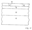
- FIGURE 17 is a view, similar to the last-described views, which illustrates an alternative manner of practicing the invention.
- Transistor 10 is an N-channel, field-effect, power-MOS transistor (semiconductor device) which has been manufactured according to one manner of practicing the steps of the present invention.
- Transistor 10 is typical in construction to like prior art devices, and includes a gate 12, a drain 14 and a source 16.
- gate 12 includes three "fingers" 12a, 12b, 12c.
- transistor 10 More specifically, in drain 14 there is a base N- doped layer 18, and an N- doped epitaxial layer 20. Also included in the structure of transistor 10 is a P-doped layer 22 which forms the so-called “body” in the transistor, and residing therein an N+ doped layer 24 which forms the source in the transistor.
- a gate-oxide layer (SiO2) 26 Residing immediately above the last-mentioned three layers is a gate-oxide layer (SiO2) 26, and two metallization layers 28, 30. These two metal layers are typically formed, and herein are formed, of aluminum. Layer 28 acts as an electrical contact for the source, and layer 30 forms previously mentioned gate 12.
- transistor 10 was formed in accordance with one manner of practicing the invention.
- Layers 18, 20 reside in the usual commercially available silicon wafer, and may be thought of herein as forming the "starting material" for the manufacture of transistor 10.
- layer 18 has a thickness of about 15-mils and a resistivity of about 0.007-0.02-ohm-centimeters.
- Epitaxial layer 20 has a thickness herein of about 36-44-microns, and a resistivity of about 16-22-ohm-centimeters.
- Gate-oxide layer 26 has a thickness herein of about 2400-Angstroms, and is conventionally thermally grown through oxidation in a diffusion furnace at a temperature of around 1100°C. Layers 18, 20, 26 herein make up what is referred to as a substrate structure.
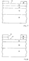
- Fig. 4 illustrates the preparation of a new layer 32 which overlies layer 26.
- This layer which ultimately disappears, as will be explained, plays a significant role both in avoiding multiple masking steps, and in controlling proper doping to create the desire junctions.
- the material in this layer must be etchable in a medium which is different than that in which layer 26 is etchable.
- layer 32 must be capable of withstanding (i.e., retaining structural integrity) at the high temperatures which characterize conventional diffusion steps.
- layer 32 must be impenetrable (100% penetration) to the doping substances which are used to form previously mentioned layers 22, 24.
- Particular materials other than polysilicon which may be used for this layer include silicon nitride, refractory-metal silicide, and doped oxides.
- a layer 34 over layer 32 is a negative photoresist.
- a positive photoresist could also be used to form this layer.
- Fig. 6 the single, independent mask which is employed herein during the photolithography steps is shown generally at 36.
- the pattern which will ultimately result in transistor 10 is suitably created in mask 36, and in Fig. 6, mask 36 can be seen to include light-transparent areas, such as area 36 a , and light-opaque areas, such as area 36 b .
- the assembly illustrated in Fig. 6 is exposed to light during a typical photolithography step, and as a consequence, the photoresist layer ends up with regions exposed (outside the dashed lines) and regions not exposed (inside the dashed lines) to light.
- Fig. 7 illustrates the next step, wherein photoresist, and specifically those regions which have not been exposed to light, is removed conventionally by a suitable photoresist developer. Such a removed region is shown generally at 38.
- Fig. 8 illustrates the next subsequent step, wherein the polysilicon layer is now etched, by any commercial etching technique, to transfer the image previously created in photoresist layer 34 into layer 32. Accordingly, a matching image for region 38 is created in layer 32, and such is indicated generally as a region at 40.
- Region 40 is referred to herein as a mask-surrogate pattern-definer, and more specifically, as a primary, mask-surrogate pattern-definer.
- the term "mask-surrogate pattern-definer" is used to point out an important operational feature of the invention, namely that through the creation of such a pattern-definer in the structure itself, one completely eliminates the need for the use of any independent mask other than mask 36. Obviously, this is an important contribution to the creation of a device free from masking-related defects, in that, such a defect can no longer develop in the structure through the subsequent processing steps.
- the pattern-definer thus formed has a defined outline (edge configuration). As will become apparent in the description which continues, this outline per se, with no alteration, is used as the only necessary self-alignment masking agency in manufacturing steps that follow.
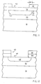
- Photoresist layer 34 is now removed by any convenient conventional technique, and this is illustrated in Fig. 9.
- Fig. 10 illustrates a first implant step, which takes the form of a boron implant that will result, as will be explained, in previously mentioned layer 22.
- the boron implant step is performed in a conventional implanter at an energy level of about 160-KEV to produce an implant density in layer 20 of about 6X10¹³-atoms-per-cubic-centimeter.
- Dashed line 42 illustrates the material implanted in layer 20 by this step, and this implant extends to a depth in layer 20 of about 0.27-micrometers. As can be seen, dashed line 42 extends laterally beyond the boundaries of pattern-definer 40, and this results from the action of the gate-oxide layer which functions as a dispersion medium.
- a dashed line shown at 44 illustrates that there is some penetration of boron into layer 32, but not a complete penetration of this layer.
- Layer 32's opaqueness to boron penetration functions, importantly, to achieve properly controlled doping in this step.
- Fig. 11 illustrates the first diffusion step, which is performed in a conventional diffusion furnace at a typical temperature of about 1150°C for about 3-8 hours.
- this diffused region has a depth, shown at 46 in Fig. 11, or about 3-6 microns.
- This region extends laterally beyond the margins of pattern-definer 40 by a dimension, shown generally at 48, which is about 60-80% of dimension 46.
- Fig. 12 illustrates the next step in the procedure, wherein layer 26 is etched by any commercial etching technique to transfer into layer 26 a matching pattern (image of first pattern-definer 40).
- a matching pattern image of first pattern-definer 40.
- Fig. 13 illustrates a second implant step which is performed herein using phosphorus.
- This step takes place in a conventional implanter at an energy level of about 160-KEV to produce a final implant density of about 5X10¹⁵ to 1X10¹⁶-atoms-per-cubic-centimeter.
- the implant which results in layer 20 is indicated by dashed line 50, and this extends to a depth, indicated at 52, of about 0.2-microns.
- dashed line 50 the implant just performed is contained completely within diffused region 22, and extends laterally slightly beyond the boundaries of pattern-definer 40.
- Dashed line 51 indicates slight penetration of phosphorus into layer 32, but nowhere complete penetration.
- dopant opaqueness in layer 32 functions significantly, as mentioned in connection with the boron doping implant step, to control and effect a proper final doped result.
- Fig. 14 illustrates the second and final diffusion step which is conducted to create transistor 10. This diffusion also takes place in a diffusion furnace, typically at a temperature of about 1100°C for about 1-3-hours. What results, completely within the region indicated at 22, is a new diffused region which will result ultimately in previously described source layer 24.
- Layer 24 has a depth dimension, shown at 54, of about 1-3-microns, and a lateral-extension dimension, shown at 56, (extension beyond the boundaries of pattern-definer 40) which is about 60-80% of dimension 54.
- this second diffusion step is the growth in region 49 of a thin oxide film 57 on the surface of layer 20. At this point in the procedure, this oxide is removed by any suitable conventional etching technique.
- Fig. 15 illustrates a subsequent step in which silicon in the upper portion of layer 20 is etched to produce the trench shown generally at 60.
- the silicon in the wafer mentioned earlier has a crystal orientation herein of ⁇ 100>.
- the etch just referred to is performed anisotropically using potassium hydroxide.
- the potassium hydroxide etch just mentioned is followed by an isotropic, planar etch using a mixture of nitric, acetic and hydrofluoric acids to remove any trace of remaining potassium, and to enlarge the trench slightly by what might be thought of as a removed wall thickness of about 0.25-0.5-microns, thus to create an overhang for the underside of layer 26. This is illustrated by dashed line 62 in Fig. 15.
- Fig. 15 also demonstrates yet another consequence of the planar etch--namely the removal of layer 32.
- Fig. 16 illustrates a final step in the manner now being described of practicing the invention.
- the step herein illustrated is the so-called metallization, or conductive-material-deposition, step where aluminum is preferably cold-evaporated to create source layer 28 and gate layer 30. It is important that this step be conducted in such a manner that metal which forms layer 28 contact layer 24, but not contact layer 30.
- transistor 10 With completion of the metallization step, the basic formation of transistor 10 is complete.
- mask-surrogate pattern-definer 40 is removal-formed directly in layer 32, either by laser-beam impingement, or by ion-beam bombardment. Also, instead of using such a technique to remove material in the formation of a mask-surrogate pattern-definer, the same technique could be employed to deposit such a pattern-definer. Thereafter, all of the other steps described earlier are performed in the same respective manners.
- Yet another advantage offered by the invention is that it eliminates the kind of defects which can result from temperature and humidity changes that occur in the working environment over the time now required to complete multiple masking steps.
- the mask-surrogate pattern-definers which are created, built into the structure as they are, eliminate these possibilities.
Landscapes
- Electrodes Of Semiconductors (AREA)
- Thin Film Transistor (AREA)
- Drying Of Semiconductors (AREA)
- Light Receiving Elements (AREA)
- Preparing Plates And Mask In Photomechanical Process (AREA)
- Insulated Gate Type Field-Effect Transistor (AREA)
- Metal-Oxide And Bipolar Metal-Oxide Semiconductor Integrated Circuits (AREA)
Claims (9)
- Procédé, utilisant un moyen de définition de dessin de substitution de masque, pour produire un dispositif MOS (10) de puissance et à effet de champ, dans une structure de substrat comprenant une couche (26) d'oxyde de grille sur la surface supérieure d'un substrat semiconducteur, ce procédé étant caractérisé par les étapes suivantes exécutées dans l'ordre donné:
formation d'une couche (32) de protection contre le dopant sur la couche (26) d'oxyde de grille;
masquage (34) de la couche de protection contre le dopant (32) et réalisation (36) d'un dessin sur cette couche par élimination sélective d'une partie de la couche de protection contre le dopant pour former un moyen (40) de définition de dessin de substitution de masque présentant une caractéristique de contour définie, de telle sorte que le moyen de définition de dessin protège une région sous-jacente (49) d'oxyde de grille et une première partie de la surface supérieure du substrat, et pour exposer une seconde partie de la surface supérieure du substrat dans une région définie par la caractéristique de contour définie;
exécution d'une première étape de dopage pour introduire un dopant (42) dans ladite seconde partie de surface supérieure exposée du substrat de manière à former une première région MOS (22), laquelle est une région de corps MOS d'un premier type de conductivité, ladite première région s'étendant sur une dimension latérale (48) en dessous du bord périphérique de la couche protectrice,
exécution d'une seconde étape de dopage pour introduire un dopant (50) dans ladite seconde surface supérieure exposée, de manière à former une seconde région MOS (24), laquelle est une région de corps MOS d'un second type de conductivité, opposé à celui de la première région MOS (22);
ladite seconde région (24) étant entièrement contenue dans ladite première région (22) et s'étendant sur une distance comprise dans ladite dimension (48) le long de la surface supérieure du substrat pour définir un canal MOS en dessous de ladite région (49) de la couche (26) d'oxyde de grille;
la couche (32) de protection contre le dopant étant opaque au dopant de manière à empêcher le dopant introduit (42, 50) de pénétrer dans la région sous-jacente (49) d'oxyde de grille;
attaque simultanée à l'acide de la couche de protection contre le dopant et de la surface supérieure exposée du substrat après les première et seconde étapes de dopage pour former une tranchée (60) dans la partie de surface supérieure exposée du substrat, la tranchée étant formée jusqu'à une profondeur de tranchée supérieure à l'épaisseur (52) de la seconde région mais inférieure à l'épaisseur (46) de la première région (22), et ayant une largeur inférieure à celle de la seconde région (24) de telle sorte que des régions séparées (24′) du second type de conductivité soient présentes au niveau des parois latérales de la tranchée, les régions séparées (24′) constituant des régions de source du dispositif MOS (10); et
dépôt d'une couche de matériau conducteur sur la totalité de la surface supérieure du dispositif pour former simultanément une première couche conductrice (28) dans la tranchée, cette couche étant en contact à la fois avec la région de source et les régions de corps pour former, entre lesdites régions, un court-circuit qui s'étend de façon continue le long des parois latérales de la tranchée, et une seconde couche conductrice (30) recouvrant la totalité de la région (49) d'oxyde de grille. - Procédé selon la revendication 1, dans lequel on réalise les parois latérales en contre-dépouille sous la région (49) d'oxyde de grille.
- Procédé selon la revendication 1 ou 2, dans lequel on forme les parois latérales de la tranchée par une attaque à l'acide,qui comprend une attaque anisotrope, pour qu'elles fassent saillie latéralement en direction l'une de l'autre, cette attaque anisotrope progressant dans le sens de la profondeur dans la tranchée (60) de telle sorte qu'une partie du substrat contenant la seconde région (24) dudit second type de conductivité soit découverte le long d'une région supérieure des parois latérales de la tranchée afin d'être en contact avec la couche conductrice.
- Procédé selon l'une quelconque des revendication 1 à 3, dans lequel on dépose la couche de matériau conducteur de telle sorte que ladite couche conductrice (28) dans la tranchée, quand elle a été déposée, soit séparée de ladite couche conductrice (30) recouvrant la région (49) d'oxyde de grille.
- Procédé selon l'une quelconque des revendications 1 à 4 dans lequel on forme la tranchée (60) jusqu'à une certaine profondeur de tranchée et on dépose la couche conductrice (28) dans la tranchée sur une certaine épaisseur par rapport à la profondeur de la tranchée pour espacer la couche conductrice (28) en dessous de la couche d'oxyde de manière que les régions séparées (24′) du substrat soient en contact le long des parois latérales de la tranchée et de manière que les deux couches conductrices précitées soient séparées du point de vue électrique le long de ladite caractéristique de contour définie.
- Procédé selon l'une quelconque des revendications 1 à 5, dans lequel la formation de la seconde région (24) dudit second type de conductivité est telle que ladite dimension latérale (48) de cette région s'étend sous le bord périphérique de la couche de protection contre le dopant sur 60% - 80% de la distance sur laquelle la première région s'étend vers le bas depuis la surface supérieure du substrat.
- Procédé selon l'une quelconque des revendications 1 à 6 dans lequel la seconde étape de dopage comprend un dopage par implantation ionique d'un dopant (50) dans la partie exposée du substrat avant la formation de la tranchée (60) de telle sorte que la tranchée divise la partie de substrat dopée en des régions de source séparées (24) s'étendant le long de chaque paroi latérale de la tranchée.
- Procédé selon l'une quelconque des revendications 1 à 7 dans lequel la couche (32) de protection contre le dopant comprend une couche de silicium polycristallin.
- Procédé selon l'une quelconque des revendications 1 à 8, dans lequel on élimine complètement la couche de dopant pendant l'étape d'attaque à l'acide pour former la tranchée de manière à découvrir la couche (26) d'oxyde de grille et on dépose la seconde couche conductrice (30) en contact direct avec la couche (26) d'oxyde de grille.
Applications Claiming Priority (2)
| Application Number | Priority Date | Filing Date | Title |
|---|---|---|---|
| US06/842,771 US4748103A (en) | 1986-03-21 | 1986-03-21 | Mask-surrogate semiconductor process employing dopant protective region |
| US842771 | 1986-03-21 |
Publications (3)
| Publication Number | Publication Date |
|---|---|
| EP0238362A2 EP0238362A2 (fr) | 1987-09-23 |
| EP0238362A3 EP0238362A3 (en) | 1988-11-30 |
| EP0238362B1 true EP0238362B1 (fr) | 1994-12-28 |
Family
ID=25288204
Family Applications (1)
| Application Number | Title | Priority Date | Filing Date |
|---|---|---|---|
| EP87302480A Expired - Lifetime EP0238362B1 (fr) | 1986-03-21 | 1987-03-23 | Procédé de fabrication de semi-conducteur à masque de substitution employant des régions opaques aux dopants |
Country Status (7)
| Country | Link |
|---|---|
| US (1) | US4748103A (fr) |
| EP (1) | EP0238362B1 (fr) |
| JP (1) | JP2575378B2 (fr) |
| KR (1) | KR960000387B1 (fr) |
| AT (1) | ATE116479T1 (fr) |
| CA (2) | CA1253262A (fr) |
| DE (1) | DE3750909T2 (fr) |
Families Citing this family (28)
| Publication number | Priority date | Publication date | Assignee | Title |
|---|---|---|---|---|
| GB2172427A (en) * | 1985-03-13 | 1986-09-17 | Philips Electronic Associated | Semiconductor device manufacture using a deflected ion beam |
| US5182234A (en) * | 1986-03-21 | 1993-01-26 | Advanced Power Technology, Inc. | Profile tailored trench etch using a SF6 -O2 etching composition wherein both isotropic and anisotropic etching is achieved by varying the amount of oxygen |
| US4895810A (en) * | 1986-03-21 | 1990-01-23 | Advanced Power Technology, Inc. | Iopographic pattern delineated power mosfet with profile tailored recessed source |
| JP2615667B2 (ja) * | 1987-09-28 | 1997-06-04 | 日産自動車株式会社 | Mos電界効果トランジスタの製造方法 |
| JPH0783122B2 (ja) * | 1988-12-01 | 1995-09-06 | 富士電機株式会社 | 半導体装置の製造方法 |
| US4970173A (en) * | 1989-07-03 | 1990-11-13 | Motorola, Inc. | Method of making high voltage vertical field effect transistor with improved safe operating area |
| US5155052A (en) * | 1991-06-14 | 1992-10-13 | Davies Robert B | Vertical field effect transistor with improved control of low resistivity region geometry |
| EP0534530B1 (fr) * | 1991-09-23 | 2000-05-03 | Koninklijke Philips Electronics N.V. | Procédé de fabrication d'un dispositif consistant à implanter une substance dans un corps |
| US5297001A (en) * | 1992-10-08 | 1994-03-22 | Sundstrand Corporation | High power semiconductor assembly |
| US5395777A (en) * | 1994-04-06 | 1995-03-07 | United Microelectronics Corp. | Method of producing VDMOS transistors |
| US5631484A (en) * | 1995-12-26 | 1997-05-20 | Motorola, Inc. | Method of manufacturing a semiconductor device and termination structure |
| GB2323703B (en) * | 1997-03-13 | 2002-02-13 | United Microelectronics Corp | Method to inhibit the formation of ion implantation induced edge defects |
| DE19840032C1 (de) | 1998-09-02 | 1999-11-18 | Siemens Ag | Halbleiterbauelement und Herstellungsverfahren dazu |
| US6218701B1 (en) * | 1999-04-30 | 2001-04-17 | Intersil Corporation | Power MOS device with increased channel width and process for forming same |
| US6825514B2 (en) * | 2001-11-09 | 2004-11-30 | Infineon Technologies Ag | High-voltage semiconductor component |
| US6819089B2 (en) | 2001-11-09 | 2004-11-16 | Infineon Technologies Ag | Power factor correction circuit with high-voltage semiconductor component |
| US20040036131A1 (en) * | 2002-08-23 | 2004-02-26 | Micron Technology, Inc. | Electrostatic discharge protection devices having transistors with textured surfaces |
| US8629019B2 (en) | 2002-09-24 | 2014-01-14 | Vishay-Siliconix | Method of forming self aligned contacts for a power MOSFET |
| US8080459B2 (en) * | 2002-09-24 | 2011-12-20 | Vishay-Siliconix | Self aligned contact in a semiconductor device and method of fabricating the same |
| ITMI20042243A1 (it) * | 2004-11-19 | 2005-02-19 | St Microelectronics Srl | Processo per la realizzazione di un dispositivo mos di potenza ad alta densita' di integrazione |
| US7875936B2 (en) * | 2004-11-19 | 2011-01-25 | Stmicroelectronics, S.R.L. | Power MOS electronic device and corresponding realizing method |
| US7544545B2 (en) | 2005-12-28 | 2009-06-09 | Vishay-Siliconix | Trench polysilicon diode |
| TWI435430B (zh) | 2006-01-18 | 2014-04-21 | 維雪 希里康尼克斯公司 | 具高靜電放電性能之低電壓輸出驅動器 |
| US8435873B2 (en) * | 2006-06-08 | 2013-05-07 | Texas Instruments Incorporated | Unguarded Schottky barrier diodes with dielectric underetch at silicide interface |
| US10600902B2 (en) | 2008-02-13 | 2020-03-24 | Vishay SIliconix, LLC | Self-repairing field effect transisitor |
| US9230810B2 (en) | 2009-09-03 | 2016-01-05 | Vishay-Siliconix | System and method for substrate wafer back side and edge cross section seals |
| JP2016051812A (ja) * | 2014-08-29 | 2016-04-11 | キヤノン株式会社 | 接合型電界効果トランジスタの製造方法、半導体装置の製造方法、撮像装置の製造方法、接合型電界効果トランジスタ及び撮像装置 |
| CN111106012B (zh) * | 2019-12-20 | 2022-05-17 | 电子科技大学 | 一种实现半导体器件局域寿命控制的方法 |
Family Cites Families (36)
| Publication number | Priority date | Publication date | Assignee | Title |
|---|---|---|---|---|
| GB1289740A (fr) * | 1969-12-24 | 1972-09-20 | ||
| NL161305C (nl) * | 1971-11-20 | 1980-01-15 | Philips Nv | Werkwijze voor het vervaardigen van een halfgeleiderin- richting. |
| US3863330A (en) * | 1973-08-02 | 1975-02-04 | Motorola Inc | Self-aligned double-diffused MOS devices |
| US4015278A (en) * | 1974-11-26 | 1977-03-29 | Fujitsu Ltd. | Field effect semiconductor device |
| FR2341943A1 (fr) * | 1976-02-20 | 1977-09-16 | Radiotechnique Compelec | Procede de realisation de transistors par implantation ionique |
| FR2454698A1 (fr) * | 1979-04-20 | 1980-11-14 | Radiotechnique Compelec | Procede de realisation de circuits integres a l'aide d'un masque multicouche et dispositifs obtenus par ce procede |
| US4383026A (en) * | 1979-05-31 | 1983-05-10 | Bell Telephone Laboratories, Incorporated | Accelerated particle lithographic processing and articles so produced |
| DE2930780C2 (de) * | 1979-07-28 | 1982-05-27 | Deutsche Itt Industries Gmbh, 7800 Freiburg | Verfahren zur Herstellung eines VMOS-Transistors |
| US4231811A (en) * | 1979-09-13 | 1980-11-04 | Intel Corporation | Variable thickness self-aligned photoresist process |
| US4545113A (en) * | 1980-10-23 | 1985-10-08 | Fairchild Camera & Instrument Corporation | Process for fabricating a lateral transistor having self-aligned base and base contact |
| JPS5793549A (en) * | 1980-12-03 | 1982-06-10 | Fujitsu Ltd | Manufacture of semiconductor device |
| US4329773A (en) * | 1980-12-10 | 1982-05-18 | International Business Machines Corp. | Method of making low leakage shallow junction IGFET devices |
| GB2102202A (en) * | 1981-07-17 | 1983-01-26 | Westinghouse Brake & Signal | Semiconductor device passivation |
| DE3279874D1 (en) * | 1981-08-21 | 1989-09-14 | Toshiba Kk | Method of manufacturing dielectric isolation regions for a semiconductor device |
| US4497107A (en) * | 1981-11-12 | 1985-02-05 | Gte Laboratories Incorporated | Method of making self-aligned high-frequency static induction transistor |
| US4437925A (en) * | 1981-11-12 | 1984-03-20 | Gte Laboratories Incorporated | Etched-source static induction transistor |
| US4375124A (en) * | 1981-11-12 | 1983-03-01 | Gte Laboratories Incorporated | Power static induction transistor fabrication |
| US4468682A (en) * | 1981-11-12 | 1984-08-28 | Gte Laboratories Incorporated | Self-aligned high-frequency static induction transistor |
| US4486943A (en) * | 1981-12-16 | 1984-12-11 | Inmos Corporation | Zero drain overlap and self aligned contact method for MOS devices |
| US4553316A (en) * | 1981-12-24 | 1985-11-19 | Texas Instruments Incorporated | Self-aligned gate method for making MESFET semiconductor |
| JPS58130575A (ja) * | 1982-01-29 | 1983-08-04 | Hitachi Ltd | 電界効果トランジスタの製造方法 |
| US4625388A (en) * | 1982-04-26 | 1986-12-02 | Acrian, Inc. | Method of fabricating mesa MOSFET using overhang mask and resulting structure |
| US4419811A (en) * | 1982-04-26 | 1983-12-13 | Acrian, Inc. | Method of fabricating mesa MOSFET using overhang mask |
| US4459605A (en) * | 1982-04-26 | 1984-07-10 | Acrian, Inc. | Vertical MESFET with guardring |
| US4503598A (en) * | 1982-05-20 | 1985-03-12 | Fairchild Camera & Instrument Corporation | Method of fabricating power MOSFET structure utilizing self-aligned diffusion and etching techniques |
| US4450041A (en) * | 1982-06-21 | 1984-05-22 | The United States Of America As Represented By The Secretary Of The Navy | Chemical etching of transformed structures |
| US4561168A (en) * | 1982-11-22 | 1985-12-31 | Siliconix Incorporated | Method of making shadow isolated metal DMOS FET device |
| US4414059A (en) * | 1982-12-09 | 1983-11-08 | International Business Machines Corporation | Far UV patterning of resist materials |
| US4586243A (en) * | 1983-01-14 | 1986-05-06 | General Motors Corporation | Method for more uniformly spacing features in a semiconductor monolithic integrated circuit |
| JPS6066862A (ja) * | 1983-09-22 | 1985-04-17 | Matsushita Electronics Corp | 縦型mosfetの製造方法 |
| JPS60128622A (ja) * | 1983-12-16 | 1985-07-09 | Hitachi Ltd | エツチング法 |
| US4644637A (en) * | 1983-12-30 | 1987-02-24 | General Electric Company | Method of making an insulated-gate semiconductor device with improved shorting region |
| US4543706A (en) * | 1984-02-24 | 1985-10-01 | Gte Laboratories Incorporated | Fabrication of junction field effect transistor with filled grooves |
| US4566172A (en) * | 1984-02-24 | 1986-01-28 | Gte Laboratories Incorporated | Method of fabricating a static induction type recessed junction field effect transistor |
| US4573257A (en) * | 1984-09-14 | 1986-03-04 | Motorola, Inc. | Method of forming self-aligned implanted channel-stop and buried layer utilizing non-single crystal alignment key |
| US4558508A (en) * | 1984-10-15 | 1985-12-17 | International Business Machines Corporation | Process of making dual well CMOS semiconductor structure with aligned field-dopings using single masking step |
-
1986
- 1986-03-21 US US06/842,771 patent/US4748103A/en not_active Expired - Lifetime
-
1987
- 1987-03-20 CA CA000532581A patent/CA1253262A/fr not_active Expired
- 1987-03-21 KR KR1019870002615A patent/KR960000387B1/ko not_active Expired - Fee Related
- 1987-03-23 AT AT87302480T patent/ATE116479T1/de not_active IP Right Cessation
- 1987-03-23 EP EP87302480A patent/EP0238362B1/fr not_active Expired - Lifetime
- 1987-03-23 DE DE3750909T patent/DE3750909T2/de not_active Expired - Lifetime
- 1987-03-23 JP JP62068747A patent/JP2575378B2/ja not_active Expired - Fee Related
-
1989
- 1989-04-24 CA CA000597651A patent/CA1277437C/fr not_active Expired - Lifetime
Non-Patent Citations (1)
| Title |
|---|
| VLSI Technology, S.M. Sze, 1983, Pub. McGraw-Hill, pp. 462-4. * |
Also Published As
| Publication number | Publication date |
|---|---|
| EP0238362A2 (fr) | 1987-09-23 |
| JP2575378B2 (ja) | 1997-01-22 |
| ATE116479T1 (de) | 1995-01-15 |
| US4748103A (en) | 1988-05-31 |
| JPS62279677A (ja) | 1987-12-04 |
| KR960000387B1 (ko) | 1996-01-05 |
| DE3750909D1 (de) | 1995-02-09 |
| DE3750909T2 (de) | 1995-05-11 |
| CA1253262A (fr) | 1989-04-25 |
| KR870009492A (ko) | 1987-10-27 |
| CA1277437C (fr) | 1990-12-04 |
| EP0238362A3 (en) | 1988-11-30 |
Similar Documents
| Publication | Publication Date | Title |
|---|---|---|
| EP0238362B1 (fr) | Procédé de fabrication de semi-conducteur à masque de substitution employant des régions opaques aux dopants | |
| US5019522A (en) | Method of making topographic pattern delineated power MOSFET with profile tailored recessed source | |
| EP0342952B1 (fr) | MOSFET de puissance délimitée par un motif topographique dont la source est encastrée avec un profil ajustable | |
| US5045903A (en) | Topographic pattern delineated power MOSFET with profile tailored recessed source | |
| US4757032A (en) | Method for DMOS semiconductor device fabrication | |
| EP0170250B1 (fr) | Transistor bipolaire et son procédé de fabrication | |
| US4874714A (en) | Method of making laterally oriented Schottky diode | |
| JPH0613617A (ja) | パワーmosfetトランジスタの製造方法 | |
| US4988632A (en) | Bipolar process using selective silicon deposition | |
| JPH02125623A (ja) | 自己整合トランジスタの製造方法 | |
| JPS6221269A (ja) | 半導体装置およびその製造方法 | |
| JPS6214459A (ja) | 半導体装置の製造方法 | |
| US4473941A (en) | Method of fabricating zener diodes | |
| US4290186A (en) | Method of making integrated semiconductor structure having an MOS and a capacitor device | |
| US4729967A (en) | Method of fabricating a junction field effect transistor | |
| US4675981A (en) | Method of making implanted device regions in a semiconductor using a master mask member | |
| US5089434A (en) | Mask surrogate semiconductor process employing dopant-opaque region | |
| JP2888749B2 (ja) | トランジスター及びその製造方法 | |
| US5256583A (en) | Mask surrogate semiconductor process with polysilicon gate protection | |
| EP0293979A2 (fr) | Structure d'oxyde isolant sans bird-beak pour circuits intégrés | |
| KR910000020B1 (ko) | 반도체장치의 제조방법 | |
| EP0405500B1 (fr) | Procédé de fabrication d'un dispositif semiconducteur | |
| US4202002A (en) | Ion-implanted layers with abrupt edges | |
| GB1595547A (en) | Method for forming very small contact windows in a semiconductor device | |
| JPH03173175A (ja) | 半導体装置 |
Legal Events
| Date | Code | Title | Description |
|---|---|---|---|
| PUAI | Public reference made under article 153(3) epc to a published international application that has entered the european phase |
Free format text: ORIGINAL CODE: 0009012 |
|
| AK | Designated contracting states |
Kind code of ref document: A2 Designated state(s): AT BE CH DE ES FR GB GR IT LI LU NL SE |
|
| PUAL | Search report despatched |
Free format text: ORIGINAL CODE: 0009013 |
|
| AK | Designated contracting states |
Kind code of ref document: A3 Designated state(s): AT BE CH DE ES FR GB GR IT LI LU NL SE |
|
| 17P | Request for examination filed |
Effective date: 19890306 |
|
| 17Q | First examination report despatched |
Effective date: 19910123 |
|
| K1C2 | Correction of patent application (partial reprint) published |
Effective date: 19870923 |
|
| GRAA | (expected) grant |
Free format text: ORIGINAL CODE: 0009210 |
|
| AK | Designated contracting states |
Kind code of ref document: B1 Designated state(s): AT BE CH DE ES FR GB GR IT LI LU NL SE |
|
| PG25 | Lapsed in a contracting state [announced via postgrant information from national office to epo] |
Ref country code: IT Free format text: LAPSE BECAUSE OF FAILURE TO SUBMIT A TRANSLATION OF THE DESCRIPTION OR TO PAY THE FEE WITHIN THE PRE;WARNING: LAPSES OF ITALIAN PATENTS WITH EFFECTIVE DATE BEFORE 2007 MAY HAVE OCCURRED AT ANY TIME BEFORE 2007. THE CORRECT EFFECTIVE DATE MAY BE DIFFERENT FROM THE ONE RECORDED.SCRIBED TIME-LIMIT Effective date: 19941228 Ref country code: BE Effective date: 19941228 Ref country code: GR Free format text: LAPSE BECAUSE OF FAILURE TO SUBMIT A TRANSLATION OF THE DESCRIPTION OR TO PAY THE FEE WITHIN THE PRESCRIBED TIME-LIMIT Effective date: 19941228 Ref country code: CH Effective date: 19941228 Ref country code: AT Effective date: 19941228 Ref country code: LI Effective date: 19941228 |
|
| REF | Corresponds to: |
Ref document number: 116479 Country of ref document: AT Date of ref document: 19950115 Kind code of ref document: T |
|
| ET | Fr: translation filed | ||
| REF | Corresponds to: |
Ref document number: 3750909 Country of ref document: DE Date of ref document: 19950209 |
|
| PG25 | Lapsed in a contracting state [announced via postgrant information from national office to epo] |
Ref country code: SE Effective date: 19950328 |
|
| PG25 | Lapsed in a contracting state [announced via postgrant information from national office to epo] |
Ref country code: LU Free format text: LAPSE BECAUSE OF NON-PAYMENT OF DUE FEES Effective date: 19950331 |
|
| PG25 | Lapsed in a contracting state [announced via postgrant information from national office to epo] |
Ref country code: ES Free format text: LAPSE BECAUSE OF FAILURE TO SUBMIT A TRANSLATION OF THE DESCRIPTION OR TO PAY THE FEE WITHIN THE PRESCRIBED TIME-LIMIT Effective date: 19950408 |
|
| REG | Reference to a national code |
Ref country code: CH Ref legal event code: PL |
|
| PLBE | No opposition filed within time limit |
Free format text: ORIGINAL CODE: 0009261 |
|
| STAA | Information on the status of an ep patent application or granted ep patent |
Free format text: STATUS: NO OPPOSITION FILED WITHIN TIME LIMIT |
|
| 26N | No opposition filed | ||
| REG | Reference to a national code |
Ref country code: GB Ref legal event code: IF02 |
|
| PGFP | Annual fee paid to national office [announced via postgrant information from national office to epo] |
Ref country code: GB Payment date: 20050323 Year of fee payment: 19 |
|
| PGFP | Annual fee paid to national office [announced via postgrant information from national office to epo] |
Ref country code: NL Payment date: 20060305 Year of fee payment: 20 |
|
| PGFP | Annual fee paid to national office [announced via postgrant information from national office to epo] |
Ref country code: FR Payment date: 20060308 Year of fee payment: 20 |
|
| PGFP | Annual fee paid to national office [announced via postgrant information from national office to epo] |
Ref country code: DE Payment date: 20060316 Year of fee payment: 20 |
|
| PG25 | Lapsed in a contracting state [announced via postgrant information from national office to epo] |
Ref country code: GB Free format text: LAPSE BECAUSE OF NON-PAYMENT OF DUE FEES Effective date: 20060323 |
|
| GBPC | Gb: european patent ceased through non-payment of renewal fee |
Effective date: 20060323 |
|
| PG25 | Lapsed in a contracting state [announced via postgrant information from national office to epo] |
Ref country code: NL Free format text: LAPSE BECAUSE OF EXPIRATION OF PROTECTION Effective date: 20070323 |
|
| NLV7 | Nl: ceased due to reaching the maximum lifetime of a patent |
Effective date: 20070323 |