EP0244577A1 - Elément Hall intégrable - Google Patents
Elément Hall intégrable Download PDFInfo
- Publication number
- EP0244577A1 EP0244577A1 EP87102488A EP87102488A EP0244577A1 EP 0244577 A1 EP0244577 A1 EP 0244577A1 EP 87102488 A EP87102488 A EP 87102488A EP 87102488 A EP87102488 A EP 87102488A EP 0244577 A1 EP0244577 A1 EP 0244577A1
- Authority
- EP
- European Patent Office
- Prior art keywords
- hall element
- semiconductor layer
- connections
- arrangements
- contact
- Prior art date
- Legal status (The legal status is an assumption and is not a legal conclusion. Google has not performed a legal analysis and makes no representation as to the accuracy of the status listed.)
- Granted
Links
Images


Classifications
-
- H—ELECTRICITY
- H10—SEMICONDUCTOR DEVICES; ELECTRIC SOLID-STATE DEVICES NOT OTHERWISE PROVIDED FOR
- H10N—ELECTRIC SOLID-STATE DEVICES NOT OTHERWISE PROVIDED FOR
- H10N52/00—Hall-effect devices
- H10N52/101—Semiconductor Hall-effect devices
-
- G—PHYSICS
- G01—MEASURING; TESTING
- G01R—MEASURING ELECTRIC VARIABLES; MEASURING MAGNETIC VARIABLES
- G01R33/00—Arrangements or instruments for measuring magnetic variables
- G01R33/02—Measuring direction or magnitude of magnetic fields or magnetic flux
- G01R33/06—Measuring direction or magnitude of magnetic fields or magnetic flux using galvano-magnetic devices
- G01R33/066—Measuring direction or magnitude of magnetic fields or magnetic flux using galvano-magnetic devices field-effect magnetic sensors, e.g. magnetic transistor
-
- G—PHYSICS
- G01—MEASURING; TESTING
- G01R—MEASURING ELECTRIC VARIABLES; MEASURING MAGNETIC VARIABLES
- G01R33/00—Arrangements or instruments for measuring magnetic variables
- G01R33/02—Measuring direction or magnitude of magnetic fields or magnetic flux
- G01R33/06—Measuring direction or magnitude of magnetic fields or magnetic flux using galvano-magnetic devices
- G01R33/07—Hall effect devices
-
- H—ELECTRICITY
- H10—SEMICONDUCTOR DEVICES; ELECTRIC SOLID-STATE DEVICES NOT OTHERWISE PROVIDED FOR
- H10B—ELECTRONIC MEMORY DEVICES
- H10B61/00—Magnetic memory devices, e.g. magnetoresistive RAM [MRAM] devices
-
- H—ELECTRICITY
- H10—SEMICONDUCTOR DEVICES; ELECTRIC SOLID-STATE DEVICES NOT OTHERWISE PROVIDED FOR
- H10N—ELECTRIC SOLID-STATE DEVICES NOT OTHERWISE PROVIDED FOR
- H10N59/00—Integrated devices, or assemblies of multiple devices, comprising at least one galvanomagnetic or Hall-effect element covered by groups H10N50/00 - H10N52/00
Definitions
- the invention relates to an integrable Hall element according to the preamble of claim 1.
- Hall elements of this type are advantageously used in electricity meters or power meters for measuring a magnetic field generated by an electrical current.
- An integrated Hall element of the type mentioned at the outset is e.g. known from EP 0 148 330 A2.
- This Hall element hereinafter referred to as vertical Hall element for short, measures a magnetic field which is effective parallel to its surface.
- the invention is based on the object, despite the presence of very thin semiconductor layers, of realizing an integrable, arbitrarily large Hall element with low non-linearity and low 1 / f noise.
- the effective length of a vertical Hall element is significantly greater than the thickness of the semiconductor layer.
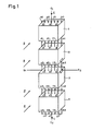
- the multi-divided Hall element shown in FIG. 1 consists of a known Hall element in the form of a right-angled parallelepiped made of semiconductor material, which has two current connections C, and C 2 and two sensor connections S, and S 2 , each on two opposite sides of the parallelepiped are arranged, the remaining two parallel sides of which are arranged perpendicular to a magnetic field H to be measured.
- This known Hall element is divided into several arrangements by at least one cut surface, the centers of the connection contacts of the sensor connections S. and S2 both lying together in a common cut surface. The cut surfaces need not be plane-parallel, nor flat and perpendicular to the current density in the Hall element.
- FIGS. 1, 2a and 2b it was assumed that there are three cut surfaces and thus four arrangements 1, 2, 3 and 4.
- FIGS. 3 to 8 the assumption applies that there is only one cutting surface and therefore two arrangements 2 and 3.
- Two points on each side of each cut surface are connected with a wire that is thought to be elastic and is electrically conductive. There are theoretically an infinite number of such points and such wires. For example, the points are all approximately on a straight line.
- Fig. 1 and in Figures 3 to 5 the presence of seven connections a to g per cut surface, in Figure 2a of five connections a to e per cut surface, in Figure 2b of three connections a to c per sectional area and in FIGS. 6 to 8 of four connections a to d per sectional area.
- the two equipotential points that must at least be present are those two points in the middle sectional area that have the same electrical potential as the sensor connections S, and S 2 . That is, each of the two external equipotential points
- the middle cut surface is to be connected to one of the two sensor connections S 1 and S 2 in such a way that it assumes its electrical potential.
- each upper and each lower surface of each arrangement 1 to 4 are each connected to an equipotential point of the opposite surface of an adjacent arrangement.
- the points of the outer surfaces of the two outer arrangements 1 and 4 selected as equipotential points are each electrically connected to one another and to the power connection C or C 2 respectively assigned to this surface, ie the eight connections a0 to g0 at the, in the illustration of the drawing , Upper surface of the upper arrangement 1 are all connected to the first power connection C, and those a4 to g4 on the lower surface of the lower arrangement 4 are all connected to the second power connection C 2 .
- a feed current I flows through the first power connection C, and the parallel connections a0 to g0 into the arrangement 1 and thus into the Hall element.
- the feed current I flows in the specified order through the arrangement 1, via the parallel connections a1 to g1, through the arrangement 2, via the parallel connections a2 to g2, through the arrangement 3, via the parallel connections a3 to g3, through the Arrangement 4 and via the parallel connections a4 to g4 to the second power connection C 2 and thus out of the Hall element.
- the through this feed current I and the magnetic field to be measured Hall voltage generated in the Hall element appears between the two sensor connections S, and S ,. It remains to be pointed out that each arrangement 1 to 4 does not represent a complete Hall element on its own.
- the arrangements 1 to 4 can be spaced apart from one another and even rotated relative to one another, on the condition that the vectorial directions of the magnetic field H, the current density in the Hall element and the electrical Hall field in the Hall element maintain their relative position (see FIGS. 2a, 3 and Fig. 5).
- the arrangements 1 to 4 are arranged approximately in a straight row next to one another, the arrangements 1 to 4 alternately not rotated (arrangements 1 and 3) or turned upside down (arrangements 2 and 4) displaced parallel so that at least the upper surfaces of the arrangements 1 to 4 finally all lie in a single common plane. All connections are parallel to each other. The relative position of the three vectorial directions mentioned has remained unchanged in relation to their original position.
- the connections a0 to e0, a2 to e2 and a4 to e4 are all arranged above and the connections a1 to e1 and a3 to e3 are all arranged below the arrangements 1 to 4.
- the integrated vertical Hall element shown in FIG. 2b represents a practical implementation of the schematic arrangement shown in FIG. 2a.
- the common plane in which the upper surfaces of the arrangements 1 to 4 lie is the surface plane of a semiconductor layer 5 in which all arrangements 1 to 4 are arranged together.
- the semiconductor layer 5 is, for. B. a thin epitaxial layer that has grown on a substrate 6.
- the connections a1 to c1 and a3 to c3 located below the arrangements 1 to 4 in the illustration of the drawing, ie part of the connections between equipotential points, each consist of a buried layer, each in the boundary layer are arranged between substrate 6 and semiconductor layer 5.
- the arrangements 1 and 2 each have the connections a1 to c1 as buried layers, which are only shown for the arrangement 2 in FIG. 2b, and the arrangements 3 and 4 each have the connections a3 to c3 as buried layers.
- each buried layer on the surface in the semiconductor layer 5 is opposite a contact diffusion.
- FIG. 2b for the arrangement 2 with 7 to 9, for the arrangement 3 with 10 to 12 and for the arrangement 4 with 13 to 15.
- a2 to c2 and a4 to c4 has one electrical contact each with one of the contact diffusions.
- These connections together form the so-called metallization of the integrated circuit and are applied to the surface of the semiconductor layer 5.
- the metallization consists of metal, for example aluminum, or of electrically conductive polysilicon.
- the metallization lies directly on this insulation layer 19, which in turn rests directly on the semiconductor layer 5.
- the connections a4 to c4 of the arrangement 4 are interconnected for the purpose of connection to their common power connection C2.
- each arrangement 1 to 4 is laterally surrounded by the neighboring arrangements with, for example, a rectangular insulation ring, two adjacent insulation rings each having a common web 16, 17 or 18.
- the insulation ring 16; 17 surrounds z. B. the arrangement 2 and the insulation ring 17; 18, for example the arrangement 3.
- the insulation rings extend from the surface of the semiconductor layer 5 to deep down, for example to spatial contact with the substrate 6.
- the substrate 6, the insulation rings and their webs 16, 17 and 18 all consist of a semiconductor material of the same material conductivity type, for example of P material. It could of course also be N-matter.
- the semiconductor layer 5, the buried layers and the contact diffusions 7 to 15 all consist of a semiconductor material of the other material conductivity type, that is to say in the example of N material.
- the buried layers and the contact diffusions 7 to 15 are all heavily doped with foreign atoms, ie they consist of N + material.
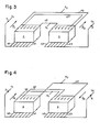
- FIG. 3 The schematic arrangement shown in FIG. 3 is similar to the arrangement shown in FIG. 2a, with the advantage that only two arrangements 2 and 3 are left, which leads to the connections to the two power connections C 1 and C 2 are located on the lower surfaces of arrangements 2 and 3 and not, as in FIG. 2a, on the upper surfaces of arrangements 1 and 4.
- the schematic arrangement shown in FIG. 4 corresponds to the arrangement shown in FIG. 3, with the difference that the connections on the surface of the arrangements 2 and 3 no longer run parallel, but crosswise.
- the magnetic field has practically rotated its relative position at the location of the arrangement 3 by 180 °. That is, the Hall element shown in FIG. 4 is no longer the sum like the Hall element shown in FIG. 3 H1 + H2 but the difference H1 H2 two magnetic fields H1 and H2 measures where H1 Magnetic field at the location of arrangement 2 and H2 .
- the magnetic field is at the location of the arrangement 3.
- a magnetic field gradient between two spatially distant points can be measured.
- the Hall element shown schematically in FIG. 5 corresponds approximately to that shown in FIG. 3, with the difference that the two arrangements 2 and 3 are not arranged approximately in a row next to one another, but rather approximately in a row one behind the other. However, the connections at the top in the illustration of the drawing run crosswise, this time to leave the relative position of the three vector directions unchanged.
- FIG. 6 shows the practical implementation of the Hall element shown schematically in FIG. 3 as an integrated circuit, again producing a vertical Hall element.
- the Hall element shown corresponds approximately to the integrated vertical Hall element shown in FIG. 2b with the difference that this time only two arrangements 2 and 3 are present.
- the points to be connected to a current connection C or C 2 on the lower surfaces of the two now outer arrangements 2 and 3 each form a single common buried layer a1; b1; c1; d1 or a3; b3; c3; d3 per arrangement 2 or 3, which each has a deep diffusion 20 or 21, which passes completely through the semiconductor layer 5, with the surface of the Hall element, ie the integrated circuit, and there with a current connection C 1 and C, respectively 2 of the Hall element are connected.
- the deep diffusions 20 and 21 consist of material which is of the same material conductivity type as the buried layers and which is heavily doped with foreign atoms, ie they consist of N + material.
- the integrated vertical Hall elements realized according to FIGS. 2b and 6 have the advantage that, in contrast to the known vertical Hall element, whose two power connections C, and C 2 are constructed very differently and have very different dimensions, they have exactly symmetrical properties in both current directions.
- the surface of the semiconductor layer 5 in FIG. 6 is covered with a thin surface layer 22.
- a thin surface layer 22 which consists of the same material P as the substrate 6. All contact diffusions 7 to 12. all webs 16 to 18 and the two deep diffusions 20 and 21 fully cross this thin Ob Surface layer 22.
- the vertical Hall element shown in FIG. 2b advantageously also has such a thin surface layer 22, which is not shown in FIG. 2b, however.
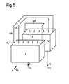
- FIGS. 7 and 8 represent the cross-section VII and the top view of the same horizontal Hall element. It also consists of two arrangements 2 and 3, which, however, are not in a row next to one another, but in plan view at an angle of approximately 90 ° to one another are arranged twisted in the semiconductor layer 5.
- the spatial arrangement and the material of the substrate 6, the semiconductor layer 5, the surface layer 22, the insulation layer 19, the metallization and the webs 16, 17 and 18 of the insulating rings, which are designated by 23 and 24 in FIG. 8, are the same as in FIG. 6. All connections a1 to d1, a2 to d2 and a3 to d3 are located as metallization on the surface of the integrated circuit. There are no buried layers this time.
- contact diffusions 25 to 32 have been replaced by contact diffusions 25 to 32, the contact diffusions 25 to 28 on the one hand and the contact diffusions 29 to 32 on the other hand advantageously being arranged approximately in a straight row.
- the contact diffusions 25 to 32 all consist of the same N + material as the contact diffusions 7 to 12.
- the connecting lines of the centers of the two contact diffusion rows 25; 26; 27; 28 and 29; 30; 31; 32 approximately form an angle of 90 ° with one another.
- Each arrangement 2 and 3 has two contact diffusion rows 25; 26; 27; 28 and 7; 8th; 9 or 10; 11; 12 and 29; 30; 31; 32, wherein in each case a contact diffusion of one row is opposite to a contact diffusion of the other row on the surface in the semiconductor layer 5.
- FIG. 8 In each of the two contact diffusion rows 7; 8th; 9 and 10; 11; 12, an unnumbered contact diffusion is drawn in FIG. 8, which lies opposite the contact diffusion 26 or 31.
- the contact diffusions 7 to 9 on the one hand and 10 to 12 on the other hand are also advantageously arranged approximately in a straight row, which is preferably parallel to the contact diffusion row 25; 26; 27; 28 and 29; 30; 31; 32.
- the connections a2 to d2 electrically connect the contact diffusions 7 to 9 to the contact diffusions 10 to 12, the connections a2 and d2 each having a sensor connection S or S 2 .
- the first current connection C, of the Hall element is connected via the connections a1 to d1 to the contact diffusions 25 to 28, which all four belong to the arrangement 2.
- the second current connection C z of the Hall element is connected to the contact diffusions 29 to 32 via the connections a3 to d3. which all four belong to arrangement 3.
- the horizontal Hall element shown in FIGS. 7 to 8 has the advantage that its zero voltage (“offset” voltage) is largely compensated for, which is explained in more detail below with reference to FIGS. 9a and 9b.
- FIG. 9a shows a bridge circuit consisting of four resistors, which represents the equivalent circuit diagram of a conventional Hall element.
- the bridge circuit contains two different resistance values R and R + AR, whereby two spatially parallel resistors, that is, two resistors diametrically opposite in the bridge circuit, are the same.
- the difference in resistance AR arises from piezoresistive effects, geometric tolerances, etc.
- the zero adjustment of the zero voltage Von can be realized in the vertical Hall element (see FIG. 3) by replacing the short-circuit connections a2 and b2 with two resistors (not shown) connected in series, the common pole of which is connected to one of the sensor connections S or S 2 is connected.
- These resistors can be implemented as adjustable trimming resistors.
- they preferably each consist of a junction field-effect transistor (JFET) or a MOS field-effect transistor, the source-drain channel resistance of which represents the resistance, the resistance value of which can be adjusted by means of the gate voltage of the field-effect transistor.
- All of the integrated Hall elements described can be produced using standard bipolar integrated circuit technology. Thanks to the use of multiple Hall elements, despite the presence of a thin epitaxial layer as the semiconductor layer 5, Hall elements of any size can be realized. This has the advantage. that the non-linearities of the Hall element are low and its 1ff noise is small.
Landscapes
- Physics & Mathematics (AREA)
- Condensed Matter Physics & Semiconductors (AREA)
- General Physics & Mathematics (AREA)
- Hall/Mr Elements (AREA)
- Measuring Magnetic Variables (AREA)
- Hard Magnetic Materials (AREA)
- Electrochromic Elements, Electrophoresis, Or Variable Reflection Or Absorption Elements (AREA)
- Cosmetics (AREA)
- Radiation-Therapy Devices (AREA)
- Magnetic Record Carriers (AREA)
- Semiconductor Integrated Circuits (AREA)
- Macromolecular Compounds Obtained By Forming Nitrogen-Containing Linkages In General (AREA)
- Pharmaceuticals Containing Other Organic And Inorganic Compounds (AREA)
Priority Applications (1)
| Application Number | Priority Date | Filing Date | Title |
|---|---|---|---|
| AT87102488T ATE59734T1 (de) | 1986-04-29 | 1987-02-21 | Integrierbares hallelement. |
Applications Claiming Priority (2)
| Application Number | Priority Date | Filing Date | Title |
|---|---|---|---|
| CH1759/86A CH669068A5 (de) | 1986-04-29 | 1986-04-29 | Integrierbares hallelement. |
| CH1759/86 | 1986-04-29 |
Publications (2)
| Publication Number | Publication Date |
|---|---|
| EP0244577A1 true EP0244577A1 (fr) | 1987-11-11 |
| EP0244577B1 EP0244577B1 (fr) | 1991-01-02 |
Family
ID=4217907
Family Applications (1)
| Application Number | Title | Priority Date | Filing Date |
|---|---|---|---|
| EP87102488A Expired - Lifetime EP0244577B1 (fr) | 1986-04-29 | 1987-02-21 | Elément Hall intégrable |
Country Status (15)
| Country | Link |
|---|---|
| US (1) | US4829352A (fr) |
| EP (1) | EP0244577B1 (fr) |
| JP (1) | JPS6393178A (fr) |
| KR (1) | KR870010391A (fr) |
| CN (1) | CN1007683B (fr) |
| AT (1) | ATE59734T1 (fr) |
| AU (1) | AU600484B2 (fr) |
| CA (1) | CA1263764A (fr) |
| CH (1) | CH669068A5 (fr) |
| DE (1) | DE3766875D1 (fr) |
| DK (1) | DK216787A (fr) |
| ES (1) | ES2019588B3 (fr) |
| FI (1) | FI871526A7 (fr) |
| NO (1) | NO871796L (fr) |
| YU (1) | YU54487A (fr) |
Cited By (8)
| Publication number | Priority date | Publication date | Assignee | Title |
|---|---|---|---|---|
| EP0503141A1 (fr) * | 1991-03-15 | 1992-09-16 | Landis & Gyr Business Support AG | Dispositif améliorant les propriétés de structures semi-conductrices comprenant des junctions PN |
| DE19857275A1 (de) * | 1998-12-11 | 2000-06-15 | Johannes V Kluge | Integrierbarer Magnetfeldsensor aus Halbleitermaterial |
| FR2829582A1 (fr) * | 2001-09-08 | 2003-03-14 | Bosch Gmbh Robert | Dispositif pour mesurer l'intensite d'une composante vectorielle d'un champ magnetique et dispositif de mesure d'une intensite de courant ainsi qu'application d'un transistor a effet de champ |
| DE10150955C1 (de) * | 2001-10-16 | 2003-06-12 | Fraunhofer Ges Forschung | Vertikaler Hall-Sensor |
| DE10150950C1 (de) * | 2001-10-16 | 2003-06-18 | Fraunhofer Ges Forschung | Kompakter vertikaler Hall-Sensor |
| EP1746426A1 (fr) * | 2005-07-22 | 2007-01-24 | Sentron Ag | Capteur de courant |
| DE102006028520B4 (de) * | 2005-06-21 | 2009-04-30 | Denso Corp., Kariya-shi | Stromsensor mit einem Hall-Element |
| EP2584304A1 (fr) * | 2011-10-21 | 2013-04-24 | Micronas GmbH | Procédé destiné à déterminer une distance et dispositif intégré de mesure de champ magnétique |
Families Citing this family (80)
| Publication number | Priority date | Publication date | Assignee | Title |
|---|---|---|---|---|
| EP0362493B1 (fr) * | 1988-09-21 | 1993-10-20 | Landis & Gyr Business Support AG | Elément de hall |
| JPH02192781A (ja) * | 1989-01-20 | 1990-07-30 | Mitsubishi Electric Corp | ホール素子および磁気センサシステム |
| JPH0390872A (ja) * | 1989-09-01 | 1991-04-16 | Toshiba Corp | 半導体装置 |
| KR0127282B1 (ko) * | 1992-05-18 | 1998-04-02 | 도요다 요시또시 | 반도체 장치 |
| EP0590222A1 (fr) * | 1992-09-30 | 1994-04-06 | STMicroelectronics S.r.l. | Capteur de position magnétique |
| US5323050A (en) * | 1993-06-01 | 1994-06-21 | Motorola, Inc. | Collector arrangement for magnetotransistor |
| JP3602611B2 (ja) * | 1995-03-30 | 2004-12-15 | 株式会社東芝 | 横型ホール素子 |
| US5572058A (en) * | 1995-07-17 | 1996-11-05 | Honeywell Inc. | Hall effect device formed in an epitaxial layer of silicon for sensing magnetic fields parallel to the epitaxial layer |
| US8397883B2 (en) * | 2001-10-25 | 2013-03-19 | Lord Corporation | Brake with field responsive material |
| AU2002322971A1 (en) * | 2002-09-10 | 2004-04-30 | Sentron Ag | Magnetic field sensor comprising a hall element |
| JP2005333103A (ja) * | 2004-03-30 | 2005-12-02 | Denso Corp | 縦型ホール素子およびその製造方法 |
| US7205622B2 (en) * | 2005-01-20 | 2007-04-17 | Honeywell International Inc. | Vertical hall effect device |
| US8169215B2 (en) * | 2006-04-13 | 2012-05-01 | Asahi Kasei Emd Corporation | Magnetic sensor and method of manufacturing thereof |
| WO2008080078A2 (fr) * | 2006-12-22 | 2008-07-03 | Lord Corporation | Frein commandable à interface d'opérateur, pourvu d'un matériau répondant à un champ magnétique |
| US20080234908A1 (en) * | 2007-03-07 | 2008-09-25 | St Clair Kenneth A | Operator input device for controlling a vehicle operation |
| CN101464479B (zh) * | 2007-12-20 | 2012-09-26 | 东光东芝测量仪器株式会社 | 电能表 |
| US7626377B2 (en) * | 2008-02-18 | 2009-12-01 | Honeywell International Inc. | Hall-effect device with merged and/or non-merged complementary structure |
| US7782050B2 (en) | 2008-04-11 | 2010-08-24 | Infineon Technologies Ag | Hall effect device and method |
| CH699933A1 (de) * | 2008-11-28 | 2010-05-31 | Melexis Technologies Sa | Vertikaler Hallsensor. |
| US8093891B2 (en) * | 2009-03-02 | 2012-01-10 | Robert Bosch Gmbh | Vertical Hall Effect sensor |
| DE102009027338A1 (de) * | 2009-06-30 | 2011-01-05 | Robert Bosch Gmbh | Hall-Sensorelement und Verfahren zur Messung eines Magnetfelds |
| DE102009029528A1 (de) * | 2009-09-17 | 2011-03-24 | Robert Bosch Gmbh | Integrierter Schaltkreis zur Informationsübertragung |
| JP5679906B2 (ja) * | 2010-07-05 | 2015-03-04 | セイコーインスツル株式会社 | ホールセンサ |
| US8896303B2 (en) | 2011-02-08 | 2014-11-25 | Infineon Technologies Ag | Low offset vertical Hall device and current spinning method |
| US8829900B2 (en) | 2011-02-08 | 2014-09-09 | Infineon Technologies Ag | Low offset spinning current hall plate and method to operate it |
| US8786279B2 (en) | 2011-02-25 | 2014-07-22 | Allegro Microsystems, Llc | Circuit and method for processing signals generated by a plurality of sensors |
| US9062990B2 (en) | 2011-02-25 | 2015-06-23 | Allegro Microsystems, Llc | Circular vertical hall magnetic field sensing element and method with a plurality of continuous output signals |
| US8729890B2 (en) | 2011-04-12 | 2014-05-20 | Allegro Microsystems, Llc | Magnetic angle and rotation speed sensor with continuous and discontinuous modes of operation based on rotation speed of a target object |
| US8860410B2 (en) | 2011-05-23 | 2014-10-14 | Allegro Microsystems, Llc | Circuits and methods for processing a signal generated by a plurality of measuring devices |
| US8890518B2 (en) | 2011-06-08 | 2014-11-18 | Allegro Microsystems, Llc | Arrangements for self-testing a circular vertical hall (CVH) sensing element and/or for self-testing a magnetic field sensor that uses a circular vertical hall (CVH) sensing element |
| DE102011107767A1 (de) * | 2011-07-15 | 2013-01-17 | Micronas Gmbh | Hallsensor |
| US8988072B2 (en) | 2011-07-21 | 2015-03-24 | Infineon Technologies Ag | Vertical hall sensor with high electrical symmetry |
| US9007060B2 (en) | 2011-07-21 | 2015-04-14 | Infineon Technologies Ag | Electronic device with ring-connected hall effect regions |
| US8793085B2 (en) | 2011-08-19 | 2014-07-29 | Allegro Microsystems, Llc | Circuits and methods for automatically adjusting a magnetic field sensor in accordance with a speed of rotation sensed by the magnetic field sensor |
| US8922206B2 (en) * | 2011-09-07 | 2014-12-30 | Allegro Microsystems, Llc | Magnetic field sensing element combining a circular vertical hall magnetic field sensing element with a planar hall element |
| US9285438B2 (en) | 2011-09-28 | 2016-03-15 | Allegro Microsystems, Llc | Circuits and methods for processing signals generated by a plurality of magnetic field sensing elements |
| US8922207B2 (en) | 2011-11-17 | 2014-12-30 | Infineon Technologies Ag | Electronic device comprising hall effect region with three contacts |
| US9046383B2 (en) | 2012-01-09 | 2015-06-02 | Allegro Microsystems, Llc | Systems and methods that use magnetic field sensors to identify positions of a gear shift lever |
| US9312472B2 (en) | 2012-02-20 | 2016-04-12 | Infineon Technologies Ag | Vertical hall device with electrical 180 degree symmetry |
| US9182456B2 (en) | 2012-03-06 | 2015-11-10 | Allegro Microsystems, Llc | Magnetic field sensor for sensing rotation of an object |
| US10215550B2 (en) | 2012-05-01 | 2019-02-26 | Allegro Microsystems, Llc | Methods and apparatus for magnetic sensors having highly uniform magnetic fields |
| US9484525B2 (en) * | 2012-05-15 | 2016-11-01 | Infineon Technologies Ag | Hall effect device |
| CN103576101A (zh) * | 2012-07-31 | 2014-02-12 | 北京嘉岳同乐极电子有限公司 | 一种多通道集成式磁传感器 |
| US9606190B2 (en) | 2012-12-21 | 2017-03-28 | Allegro Microsystems, Llc | Magnetic field sensor arrangements and associated methods |
| US9417295B2 (en) | 2012-12-21 | 2016-08-16 | Allegro Microsystems, Llc | Circuits and methods for processing signals generated by a circular vertical hall (CVH) sensing element in the presence of a multi-pole magnet |
| US8749005B1 (en) | 2012-12-21 | 2014-06-10 | Allegro Microsystems, Llc | Magnetic field sensor and method of fabricating a magnetic field sensor having a plurality of vertical hall elements arranged in at least a portion of a polygonal shape |
| US9548443B2 (en) | 2013-01-29 | 2017-01-17 | Allegro Microsystems, Llc | Vertical Hall Effect element with improved sensitivity |
| US9377285B2 (en) | 2013-02-13 | 2016-06-28 | Allegro Microsystems, Llc | Magnetic field sensor and related techniques that provide varying current spinning phase sequences of a magnetic field sensing element |
| US9389060B2 (en) | 2013-02-13 | 2016-07-12 | Allegro Microsystems, Llc | Magnetic field sensor and related techniques that provide an angle error correction module |
| US9099638B2 (en) | 2013-03-15 | 2015-08-04 | Allegro Microsystems, Llc | Vertical hall effect element with structures to improve sensitivity |
| KR102019514B1 (ko) * | 2013-06-28 | 2019-11-15 | 매그나칩 반도체 유한회사 | 반도체 기반의 홀 센서 |
| US9400164B2 (en) | 2013-07-22 | 2016-07-26 | Allegro Microsystems, Llc | Magnetic field sensor and related techniques that provide an angle correction module |
| US9312473B2 (en) | 2013-09-30 | 2016-04-12 | Allegro Microsystems, Llc | Vertical hall effect sensor |
| US9574867B2 (en) | 2013-12-23 | 2017-02-21 | Allegro Microsystems, Llc | Magnetic field sensor and related techniques that inject an error correction signal into a signal channel to result in reduced error |
| US10120042B2 (en) | 2013-12-23 | 2018-11-06 | Allegro Microsystems, Llc | Magnetic field sensor and related techniques that inject a synthesized error correction signal into a signal channel to result in reduced error |
| US9547048B2 (en) | 2014-01-14 | 2017-01-17 | Allegro Micosystems, LLC | Circuit and method for reducing an offset component of a plurality of vertical hall elements arranged in a circle |
| US9753097B2 (en) | 2014-05-05 | 2017-09-05 | Allegro Microsystems, Llc | Magnetic field sensors and associated methods with reduced offset and improved accuracy |
| US9425385B2 (en) | 2014-05-09 | 2016-08-23 | Infineon Technologies Ag | Vertical hall effect device |
| US9316705B2 (en) * | 2014-05-09 | 2016-04-19 | Infineon Technologies Ag | Vertical hall effect-device |
| US9448288B2 (en) | 2014-05-20 | 2016-09-20 | Allegro Microsystems, Llc | Magnetic field sensor with improved accuracy resulting from a digital potentiometer |
| EP2963435B1 (fr) * | 2014-07-01 | 2017-01-25 | Nxp B.V. | Système de capteur de champ magnétique latéral différentiel avec annulation de décalage et mis en oeuvre à l'aide de la technologie silicium sur isolant |
| EP2966462B1 (fr) * | 2014-07-11 | 2022-04-20 | Senis AG | Capteur à effet Hall vertical |
| GB2531536A (en) * | 2014-10-21 | 2016-04-27 | Melexis Technologies Nv | Vertical hall sensors with reduced offset error |
| US9823092B2 (en) | 2014-10-31 | 2017-11-21 | Allegro Microsystems, Llc | Magnetic field sensor providing a movement detector |
| US9638766B2 (en) | 2014-11-24 | 2017-05-02 | Allegro Microsystems, Llc | Magnetic field sensor with improved accuracy resulting from a variable potentiometer and a gain circuit |
| US9684042B2 (en) | 2015-02-27 | 2017-06-20 | Allegro Microsystems, Llc | Magnetic field sensor with improved accuracy and method of obtaining improved accuracy with a magnetic field sensor |
| US11163022B2 (en) | 2015-06-12 | 2021-11-02 | Allegro Microsystems, Llc | Magnetic field sensor for angle detection with a phase-locked loop |
| US10481220B2 (en) | 2016-02-01 | 2019-11-19 | Allegro Microsystems, Llc | Circular vertical hall (CVH) sensing element with signal processing and arctangent function |
| US9739848B1 (en) | 2016-02-01 | 2017-08-22 | Allegro Microsystems, Llc | Circular vertical hall (CVH) sensing element with sliding integration |
| US9739847B1 (en) | 2016-02-01 | 2017-08-22 | Allegro Microsystems, Llc | Circular vertical hall (CVH) sensing element with signal processing |
| US10385964B2 (en) | 2016-06-08 | 2019-08-20 | Allegro Microsystems, Llc | Enhanced neutral gear sensor |
| US10585147B2 (en) | 2016-06-14 | 2020-03-10 | Allegro Microsystems, Llc | Magnetic field sensor having error correction |
| US10739164B2 (en) | 2017-01-27 | 2020-08-11 | Allegro Microsystems, Llc | Circuit for detecting motion of an object |
| US10495701B2 (en) | 2017-03-02 | 2019-12-03 | Allegro Microsystems, Llc | Circular vertical hall (CVH) sensing element with DC offset removal |
| US10823586B2 (en) | 2018-12-26 | 2020-11-03 | Allegro Microsystems, Llc | Magnetic field sensor having unequally spaced magnetic field sensing elements |
| US11237020B2 (en) | 2019-11-14 | 2022-02-01 | Allegro Microsystems, Llc | Magnetic field sensor having two rows of magnetic field sensing elements for measuring an angle of rotation of a magnet |
| US11280637B2 (en) | 2019-11-14 | 2022-03-22 | Allegro Microsystems, Llc | High performance magnetic angle sensor |
| CN112038484B (zh) * | 2020-08-25 | 2021-06-01 | 深圳市金誉半导体股份有限公司 | 一种双霍尔传感器及其制备方法 |
| US11802922B2 (en) | 2021-01-13 | 2023-10-31 | Allegro Microsystems, Llc | Circuit for reducing an offset component of a plurality of vertical hall elements arranged in one or more circles |
| US11473935B1 (en) | 2021-04-16 | 2022-10-18 | Allegro Microsystems, Llc | System and related techniques that provide an angle sensor for sensing an angle of rotation of a ferromagnetic screw |
Citations (2)
| Publication number | Priority date | Publication date | Assignee | Title |
|---|---|---|---|---|
| EP0035103A1 (fr) * | 1980-01-18 | 1981-09-09 | Siemens Aktiengesellschaft | Dispositif integré monolithique comprenant deux sondes à effet Hall |
| EP0148330A2 (fr) * | 1983-12-19 | 1985-07-17 | LGZ LANDIS & GYR ZUG AG | Elément Hall intégrable |
Family Cites Families (10)
| Publication number | Priority date | Publication date | Assignee | Title |
|---|---|---|---|---|
| NL173335C (nl) * | 1972-06-01 | 1984-01-02 | Philips Nv | Hall-element. |
| US4141026A (en) * | 1977-02-02 | 1979-02-20 | Texas Instruments Incorporated | Hall effect generator |
| US4253107A (en) * | 1978-10-06 | 1981-02-24 | Sprague Electric Company | Integrated circuit with ion implanted hall-cell |
| JPS5748264A (en) * | 1980-08-29 | 1982-03-19 | Rohm Co Ltd | Magnetic coupler |
| JPS582084A (ja) * | 1981-06-26 | 1983-01-07 | Toshiba Corp | ホ−ル素子装置 |
| JPS58154263A (ja) * | 1982-03-09 | 1983-09-13 | Seiko Instr & Electronics Ltd | ホ−ルic |
| JPS58155761A (ja) * | 1982-03-10 | 1983-09-16 | Sharp Corp | ホ−ル効果半導体集積回路 |
| EP0090665B1 (fr) * | 1982-03-30 | 1989-05-31 | Fujitsu Limited | Dispositif semi-conducteur à mémoire |
| CH668147A5 (de) * | 1985-05-22 | 1988-11-30 | Landis & Gyr Ag | Einrichtung mit einem hallelement in integrierter halbleitertechnologie. |
| JPS62206889A (ja) * | 1986-03-07 | 1987-09-11 | Seiko Instr & Electronics Ltd | 磁気センサ |
-
1986
- 1986-04-29 CH CH1759/86A patent/CH669068A5/de not_active IP Right Cessation
-
1987
- 1987-02-10 CA CA000529383A patent/CA1263764A/fr not_active Expired
- 1987-02-21 EP EP87102488A patent/EP0244577B1/fr not_active Expired - Lifetime
- 1987-02-21 ES ES87102488T patent/ES2019588B3/es not_active Expired - Lifetime
- 1987-02-21 DE DE8787102488T patent/DE3766875D1/de not_active Expired - Fee Related
- 1987-02-21 AT AT87102488T patent/ATE59734T1/de not_active IP Right Cessation
- 1987-03-10 JP JP62053222A patent/JPS6393178A/ja active Pending
- 1987-03-27 YU YU00544/87A patent/YU54487A/xx unknown
- 1987-04-07 FI FI871526A patent/FI871526A7/fi not_active Application Discontinuation
- 1987-04-21 US US07/040,854 patent/US4829352A/en not_active Expired - Fee Related
- 1987-04-25 CN CN87102998A patent/CN1007683B/zh not_active Expired
- 1987-04-27 AU AU72106/87A patent/AU600484B2/en not_active Ceased
- 1987-04-28 DK DK216787A patent/DK216787A/da not_active Application Discontinuation
- 1987-04-28 KR KR870004114A patent/KR870010391A/ko not_active Ceased
- 1987-04-29 NO NO871796A patent/NO871796L/no unknown
Patent Citations (2)
| Publication number | Priority date | Publication date | Assignee | Title |
|---|---|---|---|---|
| EP0035103A1 (fr) * | 1980-01-18 | 1981-09-09 | Siemens Aktiengesellschaft | Dispositif integré monolithique comprenant deux sondes à effet Hall |
| EP0148330A2 (fr) * | 1983-12-19 | 1985-07-17 | LGZ LANDIS & GYR ZUG AG | Elément Hall intégrable |
Cited By (11)
| Publication number | Priority date | Publication date | Assignee | Title |
|---|---|---|---|---|
| EP0503141A1 (fr) * | 1991-03-15 | 1992-09-16 | Landis & Gyr Business Support AG | Dispositif améliorant les propriétés de structures semi-conductrices comprenant des junctions PN |
| DE19857275A1 (de) * | 1998-12-11 | 2000-06-15 | Johannes V Kluge | Integrierbarer Magnetfeldsensor aus Halbleitermaterial |
| FR2829582A1 (fr) * | 2001-09-08 | 2003-03-14 | Bosch Gmbh Robert | Dispositif pour mesurer l'intensite d'une composante vectorielle d'un champ magnetique et dispositif de mesure d'une intensite de courant ainsi qu'application d'un transistor a effet de champ |
| DE10150955C1 (de) * | 2001-10-16 | 2003-06-12 | Fraunhofer Ges Forschung | Vertikaler Hall-Sensor |
| DE10150950C1 (de) * | 2001-10-16 | 2003-06-18 | Fraunhofer Ges Forschung | Kompakter vertikaler Hall-Sensor |
| WO2003036732A3 (fr) * | 2001-10-16 | 2003-10-30 | Fraunhofer Ges Forschung | Capteur vertical a effet hall de type compact |
| WO2003036733A3 (fr) * | 2001-10-16 | 2003-10-30 | Fraunhofer Ges Forschung | Capteur vertical a effet hall |
| DE102006028520B4 (de) * | 2005-06-21 | 2009-04-30 | Denso Corp., Kariya-shi | Stromsensor mit einem Hall-Element |
| EP1746426A1 (fr) * | 2005-07-22 | 2007-01-24 | Sentron Ag | Capteur de courant |
| EP2584304A1 (fr) * | 2011-10-21 | 2013-04-24 | Micronas GmbH | Procédé destiné à déterminer une distance et dispositif intégré de mesure de champ magnétique |
| US8878524B2 (en) | 2011-10-21 | 2014-11-04 | Micronas Gmbh | Method for determining a distance and an integrated magnetic field measuring device |
Also Published As
| Publication number | Publication date |
|---|---|
| DK216787A (da) | 1987-10-30 |
| FI871526A0 (fi) | 1987-04-07 |
| AU600484B2 (en) | 1990-08-16 |
| CH669068A5 (de) | 1989-02-15 |
| DE3766875D1 (de) | 1991-02-07 |
| NO871796D0 (no) | 1987-04-29 |
| ES2019588B3 (es) | 1991-07-01 |
| CA1263764A (fr) | 1989-12-05 |
| ATE59734T1 (de) | 1991-01-15 |
| CN87102998A (zh) | 1987-11-11 |
| AU7210687A (en) | 1987-11-05 |
| YU54487A (en) | 1989-12-31 |
| NO871796L (no) | 1987-10-30 |
| FI871526A7 (fi) | 1987-10-30 |
| EP0244577B1 (fr) | 1991-01-02 |
| JPS6393178A (ja) | 1988-04-23 |
| DK216787D0 (da) | 1987-04-28 |
| CN1007683B (zh) | 1990-04-18 |
| KR870010391A (ko) | 1987-11-30 |
| US4829352A (en) | 1989-05-09 |
Similar Documents
| Publication | Publication Date | Title |
|---|---|---|
| EP0244577B1 (fr) | Elément Hall intégrable | |
| EP0148330B1 (fr) | Elément Hall intégrable | |
| EP1540748B2 (fr) | Capteur de champ magnetique pourvu d'un element a effet hall | |
| EP0204135B1 (fr) | Dispositif à circuit intégré contenant un élément Hall intégrable | |
| DE2326731C3 (de) | Halbleiteranordnung mit mehreren Hall-Elementen | |
| DE4037876C2 (de) | Laterale DMOS-FET-Vorrichtung mit reduziertem Betriebswiderstand | |
| EP0202508B1 (fr) | Dispositif à circuit intégré à élément Hall intégrable | |
| DE2426954C3 (de) | Halbleiteranordnung mit Hall-Elementen | |
| DE2334405B2 (de) | Hochintegrierte (LSI-) Halbleiterschaltung und Verfahren zur Herstellung einer Vielzahl derartiger Halbleiterschaltungen | |
| DE2852621C3 (de) | Isolierschicht-Feldeffekttransistor mit einer Drif tstrecke zwischen Gate-Elektrode und Drain-Zone | |
| DE102015208430B4 (de) | Vertikale Hall-Effekt-Vorrichtungen und System mit solchen | |
| DE68920491T2 (de) | Integrierte Halbleiterschaltung, bestehend aus einer Differenztransistorschaltung mit einem Paar von FETs. | |
| DE69602555T2 (de) | Pilot-Transistor für quasi-vertikale DMOS-Anordnung | |
| EP0362493B1 (fr) | Elément de hall | |
| DE69325994T2 (de) | Integrierte Struktur eines Strom-Fühlwiderstandes für Leistungs-MOSFET-Vorrichtungen, insbesondere für Leistungs-MOSFET-Vorrichtungen mit einer Überstrom-Selbst-Schutzschaltung | |
| DE2625989A1 (de) | Halbleiterelement | |
| DE2313196A1 (de) | Transistorppaaranordnung | |
| DE1297762B (de) | Sperrschicht-Feldeffekttransistor | |
| EP0106943B1 (fr) | Elément à effet Hall | |
| EP0693672B1 (fr) | Dispositif de mesure de longueurs ou d'angles | |
| DE102023133256B3 (de) | Halbleiter-die und entsprechendes verfahren | |
| CH683388A5 (de) | Anordnung zur Eigenschaftsverbesserung von mit P/N-Uebergängen versehenen Halbleiterstrukturen. | |
| DE3855930T2 (de) | Monolitisch integrierte Leistungsschaltung in Semibrückenkonfiguration, insbesondere für die Steuerung elektrischer Motoren | |
| DE102011086761A1 (de) | Halbleitervorrichtung | |
| EP0515815B1 (fr) | Dispositif semi-conducteur à jonction PN et arrangement d'électrodes |
Legal Events
| Date | Code | Title | Description |
|---|---|---|---|
| PUAI | Public reference made under article 153(3) epc to a published international application that has entered the european phase |
Free format text: ORIGINAL CODE: 0009012 |
|
| AK | Designated contracting states |
Kind code of ref document: A1 Designated state(s): AT BE CH DE ES FR GB IT LI NL SE |
|
| 17P | Request for examination filed |
Effective date: 19871127 |
|
| 17Q | First examination report despatched |
Effective date: 19891221 |
|
| RAP1 | Party data changed (applicant data changed or rights of an application transferred) |
Owner name: LANDIS & GYR BETRIEBS AG |
|
| GRAA | (expected) grant |
Free format text: ORIGINAL CODE: 0009210 |
|
| AK | Designated contracting states |
Kind code of ref document: B1 Designated state(s): AT BE CH DE ES FR GB IT LI NL SE |
|
| REF | Corresponds to: |
Ref document number: 59734 Country of ref document: AT Date of ref document: 19910115 Kind code of ref document: T |
|
| REF | Corresponds to: |
Ref document number: 3766875 Country of ref document: DE Date of ref document: 19910207 |
|
| GBT | Gb: translation of ep patent filed (gb section 77(6)(a)/1977) | ||
| ET | Fr: translation filed | ||
| PLBE | No opposition filed within time limit |
Free format text: ORIGINAL CODE: 0009261 |
|
| STAA | Information on the status of an ep patent application or granted ep patent |
Free format text: STATUS: NO OPPOSITION FILED WITHIN TIME LIMIT |
|
| 26N | No opposition filed | ||
| PGFP | Annual fee paid to national office [announced via postgrant information from national office to epo] |
Ref country code: CH Payment date: 19920527 Year of fee payment: 6 |
|
| PGFP | Annual fee paid to national office [announced via postgrant information from national office to epo] |
Ref country code: GB Payment date: 19930125 Year of fee payment: 7 |
|
| PGFP | Annual fee paid to national office [announced via postgrant information from national office to epo] |
Ref country code: FR Payment date: 19930204 Year of fee payment: 7 |
|
| PGFP | Annual fee paid to national office [announced via postgrant information from national office to epo] |
Ref country code: BE Payment date: 19930209 Year of fee payment: 7 |
|
| PGFP | Annual fee paid to national office [announced via postgrant information from national office to epo] |
Ref country code: AT Payment date: 19930210 Year of fee payment: 7 |
|
| PGFP | Annual fee paid to national office [announced via postgrant information from national office to epo] |
Ref country code: SE Payment date: 19930211 Year of fee payment: 7 |
|
| PGFP | Annual fee paid to national office [announced via postgrant information from national office to epo] |
Ref country code: ES Payment date: 19930212 Year of fee payment: 7 |
|
| PG25 | Lapsed in a contracting state [announced via postgrant information from national office to epo] |
Ref country code: LI Effective date: 19930228 Ref country code: CH Effective date: 19930228 |
|
| PGFP | Annual fee paid to national office [announced via postgrant information from national office to epo] |
Ref country code: NL Payment date: 19930228 Year of fee payment: 7 |
|
| PGFP | Annual fee paid to national office [announced via postgrant information from national office to epo] |
Ref country code: DE Payment date: 19930331 Year of fee payment: 7 |
|
| REG | Reference to a national code |
Ref country code: CH Ref legal event code: PL |
|
| PG25 | Lapsed in a contracting state [announced via postgrant information from national office to epo] |
Ref country code: GB Effective date: 19940221 Ref country code: AT Effective date: 19940221 |
|
| PG25 | Lapsed in a contracting state [announced via postgrant information from national office to epo] |
Ref country code: SE Effective date: 19940222 Ref country code: ES Free format text: LAPSE BECAUSE OF NON-PAYMENT OF DUE FEES Effective date: 19940222 |
|
| PG25 | Lapsed in a contracting state [announced via postgrant information from national office to epo] |
Ref country code: BE Effective date: 19940228 |
|
| BERE | Be: lapsed |
Owner name: LANDIS & GYR BETRIEBS A.G. Effective date: 19940228 |
|
| PG25 | Lapsed in a contracting state [announced via postgrant information from national office to epo] |
Ref country code: NL Effective date: 19940901 |
|
| NLV4 | Nl: lapsed or anulled due to non-payment of the annual fee | ||
| GBPC | Gb: european patent ceased through non-payment of renewal fee |
Effective date: 19940221 |
|
| PG25 | Lapsed in a contracting state [announced via postgrant information from national office to epo] |
Ref country code: FR Effective date: 19941031 |
|
| PG25 | Lapsed in a contracting state [announced via postgrant information from national office to epo] |
Ref country code: DE Effective date: 19941101 |
|
| REG | Reference to a national code |
Ref country code: FR Ref legal event code: ST |
|
| EUG | Se: european patent has lapsed |
Ref document number: 87102488.1 Effective date: 19940910 |
|
| REG | Reference to a national code |
Ref country code: ES Ref legal event code: FD2A Effective date: 19990201 |
|
| PG25 | Lapsed in a contracting state [announced via postgrant information from national office to epo] |
Ref country code: IT Free format text: LAPSE BECAUSE OF NON-PAYMENT OF DUE FEES;WARNING: LAPSES OF ITALIAN PATENTS WITH EFFECTIVE DATE BEFORE 2007 MAY HAVE OCCURRED AT ANY TIME BEFORE 2007. THE CORRECT EFFECTIVE DATE MAY BE DIFFERENT FROM THE ONE RECORDED. Effective date: 20050221 |