EP0246602A2 - Dispositif comportant une couche mince en polymère - Google Patents
Dispositif comportant une couche mince en polymère Download PDFInfo
- Publication number
- EP0246602A2 EP0246602A2 EP87107225A EP87107225A EP0246602A2 EP 0246602 A2 EP0246602 A2 EP 0246602A2 EP 87107225 A EP87107225 A EP 87107225A EP 87107225 A EP87107225 A EP 87107225A EP 0246602 A2 EP0246602 A2 EP 0246602A2
- Authority
- EP
- European Patent Office
- Prior art keywords
- group
- thin film
- carbon atoms
- recurring units
- polymer
- Prior art date
- Legal status (The legal status is an assumption and is not a legal conclusion. Google has not performed a legal analysis and makes no representation as to the accuracy of the status listed.)
- Granted
Links
Images














Classifications
-
- H—ELECTRICITY
- H10—SEMICONDUCTOR DEVICES; ELECTRIC SOLID-STATE DEVICES NOT OTHERWISE PROVIDED FOR
- H10P—GENERIC PROCESSES OR APPARATUS FOR THE MANUFACTURE OR TREATMENT OF DEVICES COVERED BY CLASS H10
- H10P14/00—Formation of materials, e.g. in the shape of layers or pillars
- H10P14/60—Formation of materials, e.g. in the shape of layers or pillars of insulating materials
- H10P14/63—Formation of materials, e.g. in the shape of layers or pillars of insulating materials characterised by the formation processes
- H10P14/6326—Deposition processes
- H10P14/6342—Liquid deposition, e.g. spin-coating, sol-gel techniques or spray coating
- H10P14/6344—Liquid deposition, e.g. spin-coating, sol-gel techniques or spray coating using Langmuir-Blodgett techniques
-
- B—PERFORMING OPERATIONS; TRANSPORTING
- B05—SPRAYING OR ATOMISING IN GENERAL; APPLYING FLUENT MATERIALS TO SURFACES, IN GENERAL
- B05D—PROCESSES FOR APPLYING FLUENT MATERIALS TO SURFACES, IN GENERAL
- B05D1/00—Processes for applying liquids or other fluent materials
- B05D1/18—Processes for applying liquids or other fluent materials performed by dipping
- B05D1/20—Processes for applying liquids or other fluent materials performed by dipping substances to be applied floating on a fluid
- B05D1/202—Langmuir Blodgett films (LB films)
-
- B—PERFORMING OPERATIONS; TRANSPORTING
- B82—NANOTECHNOLOGY
- B82Y—SPECIFIC USES OR APPLICATIONS OF NANOSTRUCTURES; MEASUREMENT OR ANALYSIS OF NANOSTRUCTURES; MANUFACTURE OR TREATMENT OF NANOSTRUCTURES
- B82Y30/00—Nanotechnology for materials or surface science, e.g. nanocomposites
-
- B—PERFORMING OPERATIONS; TRANSPORTING
- B82—NANOTECHNOLOGY
- B82Y—SPECIFIC USES OR APPLICATIONS OF NANOSTRUCTURES; MEASUREMENT OR ANALYSIS OF NANOSTRUCTURES; MANUFACTURE OR TREATMENT OF NANOSTRUCTURES
- B82Y40/00—Manufacture or treatment of nanostructures
-
- H—ELECTRICITY
- H10—SEMICONDUCTOR DEVICES; ELECTRIC SOLID-STATE DEVICES NOT OTHERWISE PROVIDED FOR
- H10D—INORGANIC ELECTRIC SEMICONDUCTOR DEVICES
- H10D64/00—Electrodes of devices having potential barriers
- H10D64/60—Electrodes characterised by their materials
- H10D64/66—Electrodes having a conductor capacitively coupled to a semiconductor by an insulator, e.g. MIS electrodes
- H10D64/68—Electrodes having a conductor capacitively coupled to a semiconductor by an insulator, e.g. MIS electrodes characterised by the insulator, e.g. by the gate insulator
- H10D64/691—Electrodes having a conductor capacitively coupled to a semiconductor by an insulator, e.g. MIS electrodes characterised by the insulator, e.g. by the gate insulator comprising metallic compounds, e.g. metal oxides or metal silicates
-
- H—ELECTRICITY
- H10—SEMICONDUCTOR DEVICES; ELECTRIC SOLID-STATE DEVICES NOT OTHERWISE PROVIDED FOR
- H10P—GENERIC PROCESSES OR APPARATUS FOR THE MANUFACTURE OR TREATMENT OF DEVICES COVERED BY CLASS H10
- H10P14/00—Formation of materials, e.g. in the shape of layers or pillars
- H10P14/60—Formation of materials, e.g. in the shape of layers or pillars of insulating materials
- H10P14/66—Formation of materials, e.g. in the shape of layers or pillars of insulating materials characterised by the type of materials
- H10P14/668—Formation of materials, e.g. in the shape of layers or pillars of insulating materials characterised by the type of materials the materials being characterised by the deposition precursor materials
-
- H—ELECTRICITY
- H10—SEMICONDUCTOR DEVICES; ELECTRIC SOLID-STATE DEVICES NOT OTHERWISE PROVIDED FOR
- H10P—GENERIC PROCESSES OR APPARATUS FOR THE MANUFACTURE OR TREATMENT OF DEVICES COVERED BY CLASS H10
- H10P14/00—Formation of materials, e.g. in the shape of layers or pillars
- H10P14/60—Formation of materials, e.g. in the shape of layers or pillars of insulating materials
- H10P14/63—Formation of materials, e.g. in the shape of layers or pillars of insulating materials characterised by the formation processes
- H10P14/6326—Deposition processes
- H10P14/6342—Liquid deposition, e.g. spin-coating, sol-gel techniques or spray coating
-
- H—ELECTRICITY
- H10—SEMICONDUCTOR DEVICES; ELECTRIC SOLID-STATE DEVICES NOT OTHERWISE PROVIDED FOR
- H10P—GENERIC PROCESSES OR APPARATUS FOR THE MANUFACTURE OR TREATMENT OF DEVICES COVERED BY CLASS H10
- H10P14/00—Formation of materials, e.g. in the shape of layers or pillars
- H10P14/60—Formation of materials, e.g. in the shape of layers or pillars of insulating materials
- H10P14/68—Organic materials, e.g. photoresists
- H10P14/683—Organic materials, e.g. photoresists carbon-based polymeric organic materials, e.g. polyimides, poly cyclobutene or PVC
-
- Y—GENERAL TAGGING OF NEW TECHNOLOGICAL DEVELOPMENTS; GENERAL TAGGING OF CROSS-SECTIONAL TECHNOLOGIES SPANNING OVER SEVERAL SECTIONS OF THE IPC; TECHNICAL SUBJECTS COVERED BY FORMER USPC CROSS-REFERENCE ART COLLECTIONS [XRACs] AND DIGESTS
- Y10—TECHNICAL SUBJECTS COVERED BY FORMER USPC
- Y10T—TECHNICAL SUBJECTS COVERED BY FORMER US CLASSIFICATION
- Y10T428/00—Stock material or miscellaneous articles
- Y10T428/31504—Composite [nonstructural laminate]
-
- Y—GENERAL TAGGING OF NEW TECHNOLOGICAL DEVELOPMENTS; GENERAL TAGGING OF CROSS-SECTIONAL TECHNOLOGIES SPANNING OVER SEVERAL SECTIONS OF THE IPC; TECHNICAL SUBJECTS COVERED BY FORMER USPC CROSS-REFERENCE ART COLLECTIONS [XRACs] AND DIGESTS
- Y10—TECHNICAL SUBJECTS COVERED BY FORMER USPC
- Y10T—TECHNICAL SUBJECTS COVERED BY FORMER US CLASSIFICATION
- Y10T428/00—Stock material or miscellaneous articles
- Y10T428/31504—Composite [nonstructural laminate]
- Y10T428/31721—Of polyimide
Definitions
- the present invention relates to a thin film of a polymer and a device having the thin film, and more particularly to a thin film formed from a modified polymer by the Langmuir-Blodgett technique and a device having the thin film.
- the LB films of the straight-chain saturated fatty acids are poor in heat resistance and mechanical strength and are not suitable for practical uses.
- polymerizing films formed from unsaturated fatty acids such as co-tricosenoic acid, ⁇ -heptadecenoic acid and a-octadecylacrylic acid, unsaturated fatty acid esters such as vinyl stearate and octadecyl acrylate, or diacetylene derivatives.
- unsaturated fatty acids such as co-tricosenoic acid, ⁇ -heptadecenoic acid and a-octadecylacrylic acid
- unsaturated fatty acid esters such as vinyl stearate and octadecyl acrylate
- diacetylene derivatives unsaturated fatty acids
- hydrophilic group-containing polymers such as polyacrylic acids, polyvinyl alcohols, polyethyl acrylates and polypeptides, also have film-forming properties.
- polyacrylic acids such as polyacrylic acids, polyvinyl alcohols, polyethyl acrylates and polypeptides
- polypeptides such as polypeptides, amino acids, amino acids, amino acids, amino acids, amino acids, amino acids, amino acids, amino acids, polyvinyl alcohols, polyethyl acrylates and polypeptides.
- films of polyimide have excellent heat resistance.
- the thickness of the films prepared, for instance, by spin coating is at least 1,000 A, usually 1 U m or more. It is very difficult to form a heat resistant polyimide film with a thickness of less than 1,000 A and with no pin-hole, and it is impossible to prepare devices having such thin polyimide films.
- a further object of the present invention is to provide a device having the above polymer thin film.
- a thin film comprising a polymer having linear recurring units wherein an organic group R 1 is combined alternately with an organic group R 2 through a bivalent bonding group, wherein each of said group R 1 and said group R 2 has a valence of at least 2 and has at least 2 carbon atoms; each of said linear recurring units having at least one hydrocarbon-containing group R 3 having 10 to 30 carbon atoms bonded with covalent bond; and a device having the same.
- a thin film comprising a polymer having a structure of 5-membered or a 6-membered hetero ring; and a device having the above thin film.
- one of materials for forming the LB film is the polymer having the linear recurring unit wherein the organic group R 1 is bonded alternately with the organic group R 2 through the bivalent bonding group, wherein each of the group R 1 and the group R. 2 has a valence of at least 2 and has at least 2 carbon atoms; each of the linear recurring units having at least one hydrocarbon-containing group R 3 having 10 to 30 carbon atoms, which may have a substituent group, with covalent bond.
- the polymer used in the invention has the linear recurring units of the formula (1), (2) or (3) as the basic skelton of the polymer.
- R 1 is the organic group having the valence of at least 2 and having at least 2 carbon atoms
- R 2 is the organic group having the valence of at least 2 and having at least 2 carbon atoms. It is preferable that at least one R1 and R 2 is a group characterized by benzenoid unsaturation having at least 6 carbon atoms.
- Each of AB and BA in the above formulas is a bivalent group produced by reacting an acid group A having a hetero atom such as 0, N, S, P or B with a basic group B having a hetero group such as O, N, S, P or B, and more particularly, is a group produced by reacting the acid group.
- A such as -COOR wherein R is an alkyl group or hydrogen atom, hereinafter the same, -COX wherein X is Cl or Br, hereinafter the same, -NCO, -NCS, -CN or -CONHR with the basic group B such as -NHR, -OR, -SR or -X.
- Examples of the group AB are, for instance, and the like.
- Examples of the group BA are, for instance, and the like.
- the groups AB and BA are not limited thereto.
- the polymer used in the present invention is a polymer in which at least one, preferably two hydrocarbon-containing group R 3 is combined with the linear recurring units of the formula (1), (2) or (3) as the backbone of the polymer with covalent bond, the group R 3 having optionally a substituent group and having 10 to 30 carbon atoms, preferably 16 to 22 carbon atoms, and the so modified polymer can be formed into a film by the LB technique.
- the three methods [I] to [III] may be carried out alone or in admixture thereof.
- the groups R 3 may be same or different.
- the groups AB and BA in which the group R 3 is substituted are not limited thereto. As shown above, according to the method [I], the group R 3 is substituted for hydrogen atom attached to nitrogen atom of the group AB or the group BA.
- Examples of the recurring units in which the group R 3 is substituted according, to the method [II] are for instance, recurring units having the formula: recurring units having the formula: recurring unit having the formula: The recurring units are not limited thereto.
- the valences of the groups R 1 and R 2 are not limited thereto, but the group R 1 and the group R 2 having the valence of up to 4 are preferred,
- the group R 3 is substituted for the atom of the group A and/or the group B which are not used for forming the recurring unit.
- each of the group R l and the group R 2 is at least bivalent group having at least two carbon atoms, preferably 5 to 20 carbon atoms. It may be an aromatic group; an alicyclic group; an aliphatic group; a group wherein an aromatic group and an aliphatic group are combined; a group wherein each of the above-mentioned groups is substituted by a monovalent group having 1 to 30 carbon atoms selected from the group consisting of an aliphatic group, an alicyclic group, an aromatic group, and a group in which an aliphatic group is combined with an alicyclic group or an aromatic group; or a group wherein each of the preceding groups is substituted by a monovalent group such as a halogen atom, nitro group, amino group, cyano group, methoxyl group or acetoxyl group, or by a group in which the above monovalent group bonds to -O-, -COO-, -NHCO-, -CO
- benzenoid unsaturation as used herein is a technical term used in.contradistinction to the quinoid structfire, as shown below, and means structures same as those of carbon rings included in usual aromatic compounds.
- each of the group R 1 and the group 2 are, for instance [whérein R 4 is (OH 2 ) 1-3 , in which R 5. is an alkyl or aryl group], [wherein R 4 is as defined above] [wherein R 4 is as defined above] and the like.
- the group R 3 is a hydrocarbon-containing group having 10 to 30 carbon atoms, preferably from 16 to 22 carbon atoms.
- a monovalent aliphatic group a monovalent group wherein an alicyclic group is combined with an aliphatic group
- a monovalent group wherein an aromatic group is combined with an aliphatic group or their substituted groups
- Preferable examples of the group R 3 are, for instance, CH CH 2 CH 2 -CH(CH 2 , wherein n is an integer of 10 to 30, preferably from 16 to 22, and l + m - n-5.
- a straight-chain aliphatic hydrocarbon group is the most preferable.
- the group R 3 is bonded with each of the recurring units with covalent bond, and may have a substituent.
- substituents are, for instance, a halogen atom, nitro group, amino group, cyano group, methoxy group, acetoxy group, and the like. It is not essential that the above-mentioned substituent is included in the group R 3 , but it is preferable that fluorine atoms are included in the group R 3 , because fluorine atoms improve the hydrophobic property as compared with hydrogen atoms. That is to say, the alkyl group as the substituent can be shortened by including fluorine atoms in the substituent of the group R 3 . For instance, when the group of the formula: C 8 F 17 ( ⁇ CH 2 ) ⁇ k is used as the group R 3 , by using the group wherein k is 2, that is the group having 10 carbon atoms, it is satisfactory possible to form a film.
- the polymers having the recurring units (1) to (75) used in the present invention may include a homopolymer comprising a single kind of recurring units, a copolymer comprising different kinds of recurring units which is considered from the formulas (1) to (75), and a mixture thereof.
- polymer used in the invention may be substituted with a hydrocarbon-containing group having 1 to 9 carbon atoms according to the method [I], [II] or [III], although it may be dispensable.
- the molecular weight of the polymer used in the present invention is not particularly limited, but it is preferable that the number average molecular weight of the polymer is from about 2,000 to about 300,000 preferably about 10,000 to 150,000.
- the number average molecular weight is less than 2,000, though the film can be formed according to the LB technique, there cannot be obtained the film having the excellent heat resistance, mechanical strength, and chemical resistance.
- the molecular weight is more than 300,000, the viscosity of the polymer is too high to form a film.
- polymer used in the invention are, for instance,
- the post reaction may be completed at a temperature not lower than 20°C.
- Acylation and amidation are usually carried out at a temperature lower than 0°C and usually about -10°C. It can, however, be preferable in this invention to carry out the acylation and the amidation at a temperature in the temperature range described above since the substituent groups, such as long chain alkyl groups, of the high polymer have a tendency to be frozen and solidified. It is a matter of course that, in the above production, starting materials having different substitutional groups can be used in combination, so as to produce a copolymer. Tetracarboxylic acid dianhydrides and diamines, which may have no substituent groups may have substituent groups containing not more than 10 carbon atoms, can also be used in an amount up to about 30 %.
- the thus obtained polymer may be separated from the reaction mixture and purified to give a material for preparing films, or to the reaction mixture may be added chloroform, benzene, or the like, after completing the reaction, if necessary, to directly make a spreading solution for preparing films.
- Films can be formed from the above polymer by any methods such as the solvent cast method, the spin coat method and the LB method.
- the LB method is preferable since the LB method can provide oriented thin films having a less amount of pin holes and can control the thickness of the films in several tens angstroms.
- the modified polymer or the mixture thereof is dissolved in a solvent such as benzene, chloroform, ethyl ether, ethyl acetate, tetrahydrofuran, dimethyl formamide, or N,N-dimethylacetoamide, and the obtained solution is coated on a substrate.
- a solvent such as benzene, chloroform, ethyl ether, ethyl acetate, tetrahydrofuran, dimethyl formamide, or N,N-dimethylacetoamide
- LB films of the invention can be formed from the above polymer by any of the so-called LB technique without restriction, e.g. the vertical dipping method (LB method), the horizontal dipping method, the revolving cylindrical method and so on (as discribed in Shin J ikken K agaku Koza, V ol. 18, "Interface and Colloid", pages 498-508).
- the LB technique is a method in which a L B material is spraed onto the surface of water and compressed at a constant surface pressure to form monomolecular layer film and the monomolecular layer is transferred onto a substrate.
- the oriented films and the thickness of the films can be controlled in sereral tens angstroms.
- the LB technique is excellent since there can be obtained thin films having a thickness of not more than 2000 A, not more than 1000 A, not more than several hundreds angstroms or several tens angstroms.
- the 0 0 films having the thickness of 10,000 A or over 10,000 A can be obtained according to the LB technique.
- the thin film can be formed from the above modified polymer alone, but when the above modified polymer is mixed with a known compound capable of forming LB films (hereinafter referred to as "known LB compound"), the film forming properties can be improved.
- known LB compound a compound containing a hydrocarbon group having from about 16 to about 22 carbon atoms and a hydrophilic group is preferred.
- the compound having the formula: CH 3 (CH 2 ) 0-1 Z wherein Z and o are as defined above is preferable for improving the film forming properties and from the point of the cost.
- the compound having unsaturated bonds have a characteristic that the polymerization is conducted by irradiating light or radiation.
- the mixing ratio of the above modified polymer to the known LB compound is not particularly limited. It is preferable that the ratio of the modified polymer to the known LB compound is from 0.2 to 2.
- a solvent such as benzene or chloroform which evaporates into a gas phase without dissolving in water, is used for spreading an LB film forming material onto the water surface.
- a solvent such as benzene or chloroform which evaporates into a gas phase without dissolving in water, is used for spreading an LB film forming material onto the water surface.
- organic polar solvent examples include, for instance, N,N-dimethylformamide, N , N -dimethylacetamide, N,N-diethylformamide, N , N -diethylacetamide, N,N-dimethylmethoxyacetoamide, dimethylsulfoxide, N-methyl-2-pyrrolidone, pyridine, dimethylsulfone, hexamethylphosphoramide, tetramethylenesulfone, dimethyltetramethylenesulfone, and the like.
- the solvent such as benzene or chloroform in combination with the organic polar solvent.
- the concentration of the precursor solution to be spread onto the water surface is not particularly limited, but is usually selected from 2 X 10 -3 to 5 X 10 -3 M.
- the substrates used for forming LB films of the invention thereon are not particularly limited, and are selected according to the uses of the formed LB film.
- the substrate used in forming the LB films are, for instance, an inorganic substrate such as glass, alumina or quartz, a metal substrate, a plastic substrate, a substrate of a semiconductor of Groups IV, III-V, II-VI of the Periodic Table such as Si, GaAs or ZnS, a substrate of a ferroelectric substance such as PbTi03, BaTi03, LiNb0 3 or LiTaO 3 , a substrate of a magnetic substance, and the like.
- the substrates may be surface-treated in a usual manner.
- a silane coupling agent especially a silane coupling agent having amino group or epoxy group, or with a chelate compound of aluminum, and to heat the treated substrate, because of improving the adhesion between the thin film of the invention and the substrate.
- the modified polymer can provide thin films having no or a little defect and having a good heat resistance by the LB method, and can provide thin films having a further improved heat resistance by partially or completely converting the polymer thin film into a polyimide.
- a five-membered ring or a six-membered ring having a hetero atom can be partially or completely ring-closed.
- Examples of the polymers completely ring-closed are as follows:
- Methods for ring-closure are not particularly limited, and, for instance, the polyimide is produced from the polymer having the recurring units (80) by heating it at a temperature of 200° to 400 o C, according to the following reaction scheme.
- the groups introduced for imparting the hydrophobic property to a polyamide acid is eliminated in the form of an alcohol. Since the eliminated alcohol can be removed away or scattered away, for instance, by conducting the conversion into polyimide in a gas stream or under vacuum at a temperature of about 200° to about 400 0 C, polyimide films having excellent heat resistance and electric insulation property can be obtained.
- a known LB compound from the above-mentioned examples which is able to be removed under the condition of a ring closure reaction.
- chemical curing agents such as acetic anhydride, pyridine and isoquinoline which have been conventionally used in converting polyamide acids into polyimides, may be used in the invention, and such means may be used in combination with thermal reaction.
- the films of the invention which are obtained by forming the built-up film from the polymer on the substrate according to the LB technique, and then, if necessary, conducting the ring-closure, have excellent heat resistance, for instance, not less than 300°C, mechanical strength, chemical resistance, electric insulation properties, and the thickness of not more than 10,000 A, e.g. 5000 A, 2000 A or 10 to 1000 A.
- the thin films of the invention have excellent properties such as a high dielectric strength of not less than 1 x 10 6 V/cm even if the film thickness is less than 1000 A, several hundreds of angstroms, or 50 to.100 A.
- thin films having a heat resistance of not less than 300°C, preferably not less than 400°C, more preferably not less than S00°C can be obtained.
- precursors wherein R 1 has a valence of 3, having structures capable of forming a 5-membered hetero ring or a 6-membered hetero ring can provide polymers having excellent heat resistance, e.g.
- the thin films of the invention can be used in various devices such as electric or electronic devices. Particularly, in the thin film having a thickness of about 50 A to several hundreds angstroms, the unique effects produced by the film thickness, e.g. the tunnel effect, are expected, and many attractive applications utilizing them become possible.
- heat resistance used herein is defined that when the dielectric property and the insulation property of a thin film are not almost changed after heating the thin film at a definite temperature for 1 hour in nitrogen stream, the thin film has a heat resistance of more than the definite temperature. Also, it is defined that when a change of an inverse capacitance of a thin film after heating the film at a definite temperature for 1 hour in nitrogen stream is within 10 %, the film has a heat resistance of more than the definite temperature.
- the weight change of the heat resistant polymer having a hetero ring prepared from a precursor after heating at a definite temperature for 1 hour in nitrogen stream is below 10 % by weight
- the thin film prepared from the polymer has a heat resistance of more than the definite temperature.
- the heat resistance of thin films can be easily estimated by infrared absorption spectra of polymer films before and after heating (that is, when there is no change between the spectrum of the polymer film before heating and that of the polymer film after heating at a definite temperature, the polymer has a heat resistance of more than the definite temperature).
- the thin films of the present invention are usable as electric and electronic devices in the field of electronics.
- MIS device devices having MIS structure wherein various semiconductors and metals are combined with insulation films-, (hereinafter referred to as "MIS device") and the M IS devices are the fundamental structual in plane electronics devices or integrated circuits.
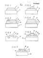
- Figs. 1 to 7 are schematic view showing typical embodiments of the MIS devices of the invention.
- Fig. 1 is a schematic view showing an MIS device wherein the thin film of the present invention is formed as an insulation film 2 on a substrate of a semiconductor 3, on which a metal 1 is provided as an electrode.
- a semiconductor of Group IV of the Periodic Table such as Si or Ge
- a semiconductor of Group III-V such as GaAs or GaP
- a semicondictor of Group II-VI such as CdTe, Cds, ZnS, ZnSe or CdHgTe
- various transducer e.g.
- photoelectric conversion element such as solar cell
- light emitting element such as LED (light emitting diode), EL (electroluminescence) or photodiode
- light receiving element light detecting element
- gas sensor temperature sensor, and the like.
- semiconductor used in the invention any of singlecrystalline semiconductors, polycrystalline semiconductors and amorphous semiconductors can be used.
- Fig. 2 is a schematic view showing an MIS device wherein 4 shows metals, 5 shows an insulation film, and 6 shows a semiconductor, having the same structure as the MIS device shown in Fig. 1 except that a plurality of metal electrodes 4 are placed on the insolution film 5.
- a plurality of metal electrodes are provided.
- charge-transfer devices such as CCD (charge-coupled device) can be prepared, which are interesting applications.
- Fig. 3 is a schematic view showing an MIS device wherein a semiconductor 9 is formed mostly in the state of a thin film on an electrode 10 which may be transparent and, of course, may be patterned, which is provided on an insulation substrate 11, insulation film 8 of the thin film of the invention is formed on the semiconductor 9, and an electrode 7 is placed on the insulation film 8.
- Fig. 4 is a schematic view showing an MIS device having the same structure as the device shown in Fig. 3 except that the thin film 14 of the invention is placed between the electrode 15 provided on the insulation substrate 16 and the thin film of the semiconductor 13.
- Fig. 4, 12 shows an electrode.
- the thin film of the semiconductor used in the invention can be prepared according to usual manners for preparing semiconductor thin films such as molecular beam epitaxy (MBE), metal organic chemical vapor deposition (MOCVD) or atomic layer epitaxy (ALE) deposition method, spatter method, spray pyrolysis method, or coating method.
- MBE molecular beam epitaxy
- MOCVD metal organic chemical vapor deposition
- ALE atomic layer epitaxy
- the preparation temperature of the MIS device is over the heat resistance of the thin film 14 of the invention since the thin film of the semiconductor 13 is formed on the thin film 14 of the invention, but it is possible to built-up amorphous silicon on the thin film conducted-the ring-closure and another semiconductors will able to be formed on the thin film with developing the film forming technique at low temperature.
- FIGs. 5 and 6 are schematic views showing typical embodiments of an MIS devices having a field effect transistor (FET) structure (hereinafter referred to as "MISFET device”), which are drived by controlling channel current with gate electrodes and which are the most important device among MIS devices.
- FET field effect transistor
- Fig. 5 is the schematic view showing the MISFET device wherein a thin film of the invention as an insulation film 18 is formed on a substate of semiconductor 21 having a source 19 and a drain 20, on which a gate electrode 17 is formed.
- Fig. 6 is the schematic view showing the MISFET device having the same structure as shown in Fig. 5 except, that a semiconductor 26 is formed mostly in the form of a thin film on a insulation substate 27.
- 22 shows a gate electrode
- 23 shows a thin film of the invention used as an insulation film
- 24 shows a source
- 25 shows a drain.
- Various electric and electronic devices can be prepared from the MISFET device, and it is one of the fundamentals.
- a thin film transistor capable of driving liquid crystal display can be prepared by using a substrate having large area, or an integrated circuit (IC) can be obtained by increasing the element number.
- IC integrated circuit
- ion-sensitive FET ISFET
- gas-sensitive FET Chem FET
- IFET immune FET
- ENFET enzyme FET
- These devices can be obtained by providing an insulation film, if necessary, with a film capable of responding ion, gas or active substances.
- the devices act due to electric field effect caused by acting the ion, gas or active substances with the surface of the gate insulation film.
- the thin film of the invention is more advantageous than conventional inorganic thin films upon further modifying the thin film with various organic substances.
- the interaction between the hydrophobic property of alkyl group and the hydrophobic part of proteins can be utilized.
- Fig. 7 is a schematic view showing the ISFET wherein the semiconductor film 32 is formed on a quartz substrate 33 as an insulation substrate, on which the ion-sensitive film 28 and the thin film of the invention 29 as an insulation film are formed.
- Fig. 7 30 shows a source and 31 shows a drain.
- the effect of the present invention can be exhibited.
- the obtained devices have a metal-semiconductor FET (MESFET) structure from the point that insulation films having good properties cannot be obtained.
- the devices having MIS structure can be obtained and the improvement of the properties of the devices can be expected by utilizing MIS structure.
- the MIS integrated circuits are prepared by using GaAs, not only the effect of lowering the driving voltage is obtained but also there can be easily obtained integrated circuits capable of driving at high speed (HEMT) which utilize large carrier mobility in the GaAs semiconductor.
- HEMT high speed
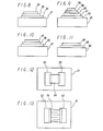
- Figs. 8 to 10 are schematic view showing typical embodiments of the devices having the MIM structure wherein a metal, an insulation film and a metal are formed in order on an insulation substrate or a semiconductor substrate.
- 34 and 36 show metals
- 35 shows an insulation film and 37 shows an insulation substrate
- 38, 40 and 42 show metals
- 39 and 41 shows insulation films and 43 shows an insulation substrate
- 44 and 46 show metals
- 45 shows an insulation film and 47 shows a semiconductor.
- Fig. 8 is a schematic view of a capacitor. There is provided a moisture sensor in case that the change of capacitance due to moisture is tracked and also there is provided a transistor having the MIM structure by utilizing the structure shown in Fig. 8.
- the MIM device is used as a capacitor of a memory cell in VLSI by forming the capacitor on a semiconductor or a semiconductor device, as shown in Fig. 10.
- a semiconductor or a semiconductor device as shown in Fig. 10.
- JJ Josephson Junction
- Fig. 11 is a schematic view showing a device having an IM structure wherein the thin film 48 of the invention is formed on the metal 49 as the insulation film, which is placed on an insulation substrate.
- the IM device is applied to liquid crystal orientation film obtained by forming the thin film of the present invention on a patterned electrode, usually a transparent electrode such as ITO.
- the IM device is used as a moisture sensor or gas senstor by forming the thin film 54 of the invention on or under two electrodes 52 and 53 shown in Figs. 12 and 13 wherein 51 shows an insulation substrate.
- the films of the invention have the reactivity to heat
- the films can be patterned by utilizing the reactivity to heat, that is, by obtaining the thin film partially ring-closed with heating and removing a part of the thin film which is not ring-closed with a solvent.
- the remainder can be used as a resist film, since the remainder is excellent in heat resistance, mechanical strength, and chemical resistance. It is possible that the thin film of the invention become have the reactivity to light by using the polymer having a double bond or triple bond in the alkyl chain.
- the films of the invention can be utilized as a cladding material for waveguide and a component for optical circuit.
- the optical circuits can be prepared by patterning the film in the same manner as above.
- the film thickness can be exactly controlled and the index of refraction can be controlled by changing the compound used in the thin film of the invention, which are very important factors in the optical circuits.
- the thin films of the invention are suitable as protective coating materials in various fields.
- various functionalities can be revealed and the uses utilizing them are considered.
- photoelectric devices and biosensors can be fabricated by forming films containing pigments or enzymes.
- the thin films of the invention are applied to a material separation. Recently, there have been many attempts utilizing thin films for material separation, the thin films having fine holes and being formed on a substrate of porous film.
- the thin films of the invention are prepared in the presence of the known LB compounds and then the ring-closure is conducted to give thin films having fine holes. For instance, a polyimide precursor is formed into a film in the presence of excess stearic alcohol on a porous polyimide film and then the conversion of the precursor into polyimide is conducted at a temperature of 300° to 400°C to give a polyimide thin film having fine holes, formed on porous polyimide film.
- a flask was charged with 2.18 g (0.01 mole) of pyromellitic dianhydride and 5.40 g (0.02 mole) of stearyl alcohol, and they were reacted at about 100°C for 3 hours in a dry nitrogen stream.
- the resulting reaction product was dissolved in 40 ml of hexamethylphosphoramide and cooled to 0° to 5°C. To the solution was added dropwise 2.38 g of thionyl chloride at about 5°C. After the completion of the addition, the solution was maintained at about 5°C for 1 hour to complete the reaction.
- reaction mixture was then added dropwise 2 g (0.01 mole) of diaminodiphenyl ether dissolved in 50 ml of dimethylacetamide at a temperature of 0° to 5°C, and after the completion of the addition, the reaction was further continued for 1 hour.
- the reaction mixture was poured into 600 ml of distilled water to precipitate the reaction product.
- the precipitate was filtered and dried under reduced pressure at about 40°C to give about 9 g of a light yellow powder.
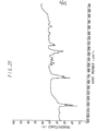
- the thermal analysis of the product was also conducted by raising the temperature to 400°C at a rate of 10 0 C/minute, maintaining the temperature at 400°C for 1 hour, dropping the temperature to room temperature and raising the temperature again to 1,000°C at a rate of 10°C/minute. The results are shown in Fig. 16.
- the number average molecular weight of the product measured by using N,N-dimethylacetamide as a solvent was about 50,000 (calculated in terms of polystyrene).
- a solution of a polymer to be spread onto the surface of water for forming a monomolecular film was prepared by dissolving 55.1 mg of the product obtained in Example 1 in a mixed solvent of distilled chloroform and dimethylacetamide in a ratio of 8 : 2 by volume so that the total volume was 25 ml.
- the obtained solution was spread onto the surface of bidistilled water, and the relationship between the surface pressure (7L) and the area per recurring unit (unit) was measured at 20°C. The result is shown in Fig. 17.
- the surface pressure suddenly increased from about 75 ⁇ 2 /unit and a good condensed film was formed.
- the limiting area was 60 ⁇ 2 /unit, and collapse pressure was 55 dyne/cm which was very high for a polymer film.
- the monolayer on the water surface was so stable that even if it was maintained on the water surface with keeping the surface pressure at 25 dyne/cm, no decrease in area was observed over 2 hours.
- a built-up film of 60 layers was formed on a glass substrate or a CaF 2 plate substrate according to the LB method by raising and lowering the substrate through the water surface at a speed of 10 mm/minute, while maintaining the surface pressure of the monolayer on the water surface at 25 dyne/cm at 20°C.
- the film formed on the CaF 2 plate was analyzed by FT-IR analysis.
- n ⁇ 2d sin ⁇
- n is a positive integer
- ⁇ is a wave length
- d is a lattice spacing
- e is Bragg angle.
- n 3 and ⁇ of X-ray is 1.5418 A
- d that is, the thickness of the monomolecular layer is calculated as 28.5 A.
- the calculated value almost agrees to an value calculated supposing that a long chain alkyl group in an amphiphilic precursor of polyimide is perpendicularly standed.
- the built-up film was heated at 400°C for 1 hour, and subjected to FT-IR analysis. From the presence of peaks at 1,790 and 1,710 cm -1 in the IR spectrum, it was confirmed that imide with ⁇ , ⁇ -unsaturated 5-membered ring was produced.
- a polymer was prepared in the same manner as in Example 1 except that n-decyl alcohol (n-C 10 ,H 21 OH) was used instead of stearyl alcohol.
- the results of IR analysis, thermal analysis and measurement of molecular weight by GPC of the obtained polymer showed approximately the same characteristics as those of the product obtained in Example 1, but the surface pressure-area curve thereof was different.
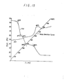
- the surface pressure-area curve is shown in Fig. 19.
- the obtained polymer showed only a liquid expansion phase, and did not show the presence of a condensed monomolecular layer. From this result, it is understood that the introduction of an alkyl group having 10 carbon atom into a polyamide acid is too short in chain length to obtain a stable monomolecular layer. For instance, the film maintained at 20 dyne/cm in surface pressure on the water surface was unstable, thus the polymer obtained in this example did not give a good built-up film.
- Polymers were prepared in the same manner as in Example 1 except that lauryl alcohol (C 12 ), myristyl alcohol (C 14 ) or cetyl alcohol (C 16 ) was used instead of stearyl alcohol.
- the obtained polymer by using the C1 2 or C 14 alcohol showed behaviors intermediate between those for C10 and C18 , and formed a sufficiently stable monolayer and could form a built-up film.
- the polymer obtained by using the Cl6 alcohol formed a very stable monolayer on the water surface and could form a good built-up film as well as the polymeS obtained by using the C 18 alcohol.
- the number average molecular weight measured using a chloroform/N,N-dirnethylacetamide mixed solvent in a volume ratio of 8/2 was about 15,000 (calculated in terms of polystyrene).
- Example 6 In a distilled chloroform/dimethylacetamide mixed solvent in a volume ratio of 8/2 was dissolved 55.1 mg of the product obtained in Example 6 to give 25 ml of a solution of the polymer to be used for forming the LB film.
- the obtained solution was spread onto the surface of bidistilled water, and the relationship between the surface pressure and the area per recurring unit was measured at 20 0 C. The result is shown in Fig. 22.
- the surface pressure suddenly increased from about 65 A /unit and a good condensed monolayer was formed.
- the limiting area was about 55 A/unit and the collapse pressure was 45 dyne/cm (Fig. 22-A).
- a solution of stearyl alcohol having the same molar concentration as the above polymer solution was mixed with the polymer solution in an amount of an equal volume to the polymer solution, and relationship between the surface pressure and the area per recurring unit was measured under the condition that the total amount of the number of the recurring units of the product obtained in Example 6 and the number of the molecules of stearyl alcohol is equalized to the number of the recurring units of the product obtained in Example 6 using no stearyl alcohol (Fig. 22-A). The result is shown in Fig. 22-B. It is understood that by adding stearyl alcohol to the solution of the polymer, the film is stabilized, since the surface pressure more suddenly increases and the collapse pressure rises to about 60 dyne/cm.
- a multilayer film was formed on a germanium sabstrate from a mixture of the product in Example 6 and stearyl alcohol in a molar ratio of 1 : 1, and the built-up film was heated in a nitrogen stream at 400°C for 1 hour. It was observed by FT-IR method that the stearyl group disappeared and the absorptions of 5-membered ring imide appeared at 1,790 cm 1 and 1,710 cm -1 . cm
- the relationship between the surface pressure and the area per recurring unit were measured in the same manner as in Example 7 except that, instead of stearyl alcohol, stearic acid, ⁇ -heptadecene acid or octadecane was used. In all of the above cases, the surface pressure more suddenly increased than the solution having the polymer alone and the collapse pressure rised, similarly to the case using stearyl alcohol.
- the values of the collapse pressures of the film prepared from the mixture of the polymer and stearic acid or the mixture of the polymer and heptadecene acid are similar to the value of the film prepared from the mixture of the polymer and stearic alcohol, and are more excellent than the value of the film prepared from the mixture of the polymer and octadecane.
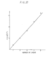
- the capacitance was measured at room temperature and at a frequency of 1 K H z.
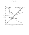
- the inverse capacitance values were plotted with respect to the number of layers. The result is shown in Fig. 23 wherein bars indicate the distribution of 10 data.
- the loss factors of the all films were about 0.02.
- A4/ heat resistance polyimide thin film/Al devices having a device area of 0.18 cm 2 were prepared by forming built-up films of 11, 21, 31, 51, 101 and 151 layers on an aluminum electrods, heating the films in a nitrogen stream at 400°C for 1 hour.
- the thicknesses of the respective polyimide films were about 50, 100, 150, 200, 250, 500 and 750 angstroms.
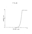
- the current-voltage curve of the device having the heat resistant polyimide film of about 100 A in thick are shown in Figs. 24 and 25. As shown in Figs. 24 and 25, it was obvious that the Ohmic conductance was shown until the electric field is 0.5 X 10 V/cm and the conductance according to In I ⁇ V 1 ⁇ 2 was shown over the above range. Also, as shown in Fig. 25, the thin film having the thickness of about 100 A can withstand 10 V, that is, the electric field of 1 X 10 7 V/ em.
- the thin film of the present invention can used as the insulating film in various electric and electronic elements.
- ZnS(Mn) layers on a patterned ITO glass having a sheet resistance of 15 ⁇ / ⁇ and a visible light transmittance of about 80 %, using ZnS having 0.7 % of Mn as a target, according to electron beam deposition under the conditions of about 1 x 10⁻⁶ torr in pressure, about 170°C in a substrate temperature 0 and about 10 A/sec in film forming speed.
- the obtained ZnS(Mn) thin film had a thickness of 0.1 um and was a polycrystalline film having a preferential orientation of (111) direction.
- the thin film was treated in nitrogen stream at 600°C for 1 hour.
- the built-up film of 21 layers were formed on the above film by using a mixture of the polymer obtained in Example 6 and stearyl alcohol in a molar ratio of 1 : 1 in the same conditions as in Example 9.
- a Y-type film was formed on ZnS(Mn) layer in a nearly ideal state. After drying overnight, the sample was heated in nitrogen stream at 400°C for 1 hour to convert the polymer into polyimide and aluminum electrode was formed by deposition on the surface of the obtained polyimide film so as to cross at a right angle with respect to the ITO electrode to give an EL device of MIS structure.
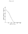
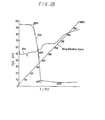
- the brightness-voltage curve as to two devices were plotted in case of applying direct current voltage (d.c. voltage) to ITO at plus and aluminum at minus.
- the results of the two typical devices are shown in Fig. 26.
- the threshold voltage was 13 V and the maximum brightness was 11 fL (at 21 V), with emission of a yellowish orange light. Also, even if the device was heated at 150°C for 30 minutes, the initial performance was not changed.
- Al/heat resistant polyimide thin film heat treated/Al devices were produced by depositing an aluminum on the heat treated films to form an electrode.
- the dielectric properties and insulation properties such as specific resistivity and dielectric breakdown strength of the above device having the heat treated thin film were similar to those of the device having the thin film which was not heat treated, and accordingly, it was obvious that the heat resistant thin film of the invention had a heat resistance of more than 400°C.
- the obtained powder was subjected to IR analysis, thermal analysis and the measurement of molecular weight by GPC.
- the number avergae molecular weight measured in the same manner as in Example 6 was about 7,000 (calculated in terms of polystyrene).
- Example 12 In a chloroform/dimethylacetamide mixed solvent in a volume ratio of 19/1 was dissolved 17.3 mg of the product obtained in Example 12 to give 10 ml of a solution to be used for forming the LB film.
- Fig. 29 (as the curve A).
- the curve A is expansive and the film was collapsed at the surface pressure of about 30 dyne/cm.
- Polymers were prepared by reacting a compound of group A with a compound of group B shown in the following Table 1 in the same manner as in Example 1, 6 or 12.
- the identification of the obtained polymers were carried out according to IR spectrum analysis and l H -N M R analysis. Also, the polymers had the same results of the thermal analysis and the measurement of molecular weight by GPC as those of the polylmers obtained in Example 1, 6 or 12. Particularly, it was confirmed that in each of the polymers obtained in Examples 16 to 22, the ring-closure and the elimination of stearyl alcohol (in case of the polymer obtained in Example 18, distearyl ether probably was eliminated) occured by heating the polymer at 300° to 400°C to form the heat resistant ring structure. Further, it was confirmed that a stable monolayer could be formed on the surface of water from each of the polymers obtained in Examples 14 to 22 and the film could be transferred to a substrate according tc LB method in the same manner as in Example 2, 7 or 13.
- the polymers modified so as to form films according to the LB method provide further stable films on the surface of water, and good built-up films are formed on substrates. Also, by heating the films to ring-close partially or completely and to eliminate the known LB compound from the films, there can be obtained the ultrathin films having good heat resistance, chemical resistance and mechanical properties, and having a thickness of not more than 10,000 A, and if desired, a thickness of 10 to 1000 A, which is hard to prepare usually.
- various devices utilizing the thin films of the present invention can be prepared.
- the thin films having a thickness of not more than 1000 A and good insulation properties are important as the insulation film for electric and electronic elements, that is, the thin films of the invention have effects that the driving voltage of the device is lowered and that the dielectric breakdown strength of the device is improved.
- the thin films of the present invention there can be prepared devices utilizing the unique effects such as hot electrons produced in insulation films having high electric field and the tunnelling effect.
- a built-up film of 61 layers was formed on an aluminum deposited substrate according to LB method by using a mixture of the polymer obtained in Example 17 and stearyl alcohol in a molar ratio of 1 : 1 (Example 23), a mixture of the polymer obtained in Example 19 and stearyl alcohol in a molar ratio of 1 : 1 (Example 24), or the polymer obtained in Example 20.
- the obtained films were good Y-types and good built-up films with a deposition ratio of about 1.
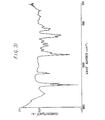
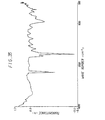
- FT-IR spectrum of each of the obtained built-up films is shown in Fig. 30 (Example 23), Fig. 31 (Example 24) or Fig. 32 (Example 25), and the same characteristic absorption as the polymer obtained in Example 17, 19 or 20 is observed.
- the built-up film was heated at 300°C (Example 23), at 450°C (Example 24) or at 400°C (Example 25) in a nitrogen stream for 1 hour, and subjected to FT-IR analysis.
- the spectra are shown in Figs. 33 (Example 23), 34 (Example 24) and 35 (Example 25), respectively.
- a polyamide acid was prepared by reacting a compound A with a compound B shown below.
- the obtained polyamide acid was converted into a lithium salt with lithium acetate and then was esterified with stearyl bromide.
- the structure of the obtained polymer was as follows: The identification of the polymer was carried out by means of IR spectrum analysis, elemental analysis and thermal analysis.
- the polymer was converted into a polymer having a heat resistant ring structure (polybenzoxadinone) shown below by heating to 300°C to 400°C to ring-close.
- a Y-type built-up film was formed by using a mixture of the obtained polymer (91) and stearyl alcohol in a molar ratio of 1 : 2 according to LB method. From FT-IR spectrum analysis, it was confirmed that a polybenzoxazinone thin film was formed by beating the built-up film.
- the thin film prepared from the above mixture was heated in a nitrogen stream at 300° C for 1 hour and was further heated in a nitrogen stream at 300°C for 1 hour, on which aluminum was deposited on the film to form an electrode to give an Al/heat-treated heat resistant polyamide-imide thin film/At device.
- the dielectric property and the insulation property of the device having the heat treated film were similar to those of the device having the thin film which was not heat treated, and accordingly, it was obvious that the heat resistant polyamide imide thin film had a heat resistance of more than 300°C.
- MIM devices were prepared in the same manner as in Example 27 except that a mixture of the polymer obtained in Example 20 and stearyl alcohol was used instead of the mixture of the polymer obtained in Example 17 and stearyl alcohol.
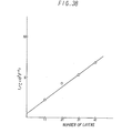
- the capacitance was measured at room temperature and at a fraquency of 120 Hz.
- the inverse capacitance values were plotted with respect to the number of layers. The result is shown in Fig. 39. It shows a good linear relationship.
- a thin film prepared from the above mixture was heated in a nitrogen stream at 5000C for 1 hour and was further heated at 500°C for 1 hour, on which aluminum was deposited to give an Al/heat treated heat resistant polyimide-isoindroquinazolinedione thin film/Al device.
- the dielectric property and the insulation property of the device having the heat treated thin film were similar to those of the device having the thin film which was not heat treated, and accordingly, it was obvious that the heat resistant polyimide-isoindroquinazolinedione thin film had a heat resistance of more than 500°C.
Landscapes
- Engineering & Computer Science (AREA)
- Chemical & Material Sciences (AREA)
- Nanotechnology (AREA)
- Condensed Matter Physics & Semiconductors (AREA)
- Physics & Mathematics (AREA)
- General Physics & Mathematics (AREA)
- Crystallography & Structural Chemistry (AREA)
- Materials Engineering (AREA)
- Composite Materials (AREA)
- Manufacturing & Machinery (AREA)
- Macromolecular Compounds Obtained By Forming Nitrogen-Containing Linkages In General (AREA)
- Manufacture Of Macromolecular Shaped Articles (AREA)
- Laminated Bodies (AREA)
- Formation Of Insulating Films (AREA)
- Polymers With Sulfur, Phosphorus Or Metals In The Main Chain (AREA)
- Application Of Or Painting With Fluid Materials (AREA)
Applications Claiming Priority (4)
| Application Number | Priority Date | Filing Date | Title |
|---|---|---|---|
| JP116391/86 | 1986-05-20 | ||
| JP11639086 | 1986-05-20 | ||
| JP11639186 | 1986-05-20 | ||
| JP116390/86 | 1986-05-20 |
Publications (3)
| Publication Number | Publication Date |
|---|---|
| EP0246602A2 true EP0246602A2 (fr) | 1987-11-25 |
| EP0246602A3 EP0246602A3 (fr) | 1991-01-02 |
| EP0246602B1 EP0246602B1 (fr) | 1994-09-28 |
Family
ID=26454727
Family Applications (1)
| Application Number | Title | Priority Date | Filing Date |
|---|---|---|---|
| EP19870107225 Expired - Lifetime EP0246602B1 (fr) | 1986-05-20 | 1987-05-19 | Dispositif comportant une couche mince en polymère |
Country Status (4)
| Country | Link |
|---|---|
| US (1) | US4839219A (fr) |
| EP (1) | EP0246602B1 (fr) |
| CA (1) | CA1302675C (fr) |
| DE (1) | DE3750591T2 (fr) |
Cited By (7)
| Publication number | Priority date | Publication date | Assignee | Title |
|---|---|---|---|---|
| WO1989003588A1 (fr) * | 1987-10-09 | 1989-04-20 | Hughes Aircraft Company | DISPOSITIFS DE CIRCUITS ELECTRIQUES GaAs AVEC COUCHE ISOLANTE LANGMUIR-BLODGETT |
| EP0237017A3 (en) * | 1986-03-11 | 1990-03-28 | Kanegafuchi Kagaku Kogyo Kabushiki Kaisha | Electric-electronic device including polyimide thin film |
| EP0239980A3 (fr) * | 1986-04-01 | 1990-04-11 | Kanegafuchi Kagaku Kogyo Kabushiki Kaisha | Dispositif électrique-électronique incluant une couche mince en polyimide |
| EP0354432A3 (fr) * | 1988-08-12 | 1991-04-10 | Bayer Ag | Supports revêtus ayant un revêtement ultramince à une ou plusieurs couches, leur procédé de fabrication et polyuréthanes comme intermédiaires pour les supports revêtus |
| US5079179A (en) * | 1987-10-09 | 1992-01-07 | Hughes Aircraft Company | Process of making GaAs electrical circuit devices with Langmuir-Blodgett insulator layer |
| US5246784A (en) * | 1990-10-09 | 1993-09-21 | Basf Aktiengesellschaft | Ultrathin thermostable bismaleimide films and production thereof |
| WO1998008086A1 (fr) * | 1996-08-23 | 1998-02-26 | Eugen Ermantraut | Nouveaux types de films minces pour la technique des microsystemes et la microstructuration, et leur utilisation |
Families Citing this family (18)
| Publication number | Priority date | Publication date | Assignee | Title |
|---|---|---|---|---|
| GB8322418D0 (en) * | 1983-08-19 | 1983-09-21 | Emi Ltd | Humidity sensor |
| US4988570A (en) * | 1985-09-11 | 1991-01-29 | Kanegafuchi Kagaku Kogyo Kabushiki Kaisha | Process for forming a film |
| US4943471A (en) * | 1986-05-20 | 1990-07-24 | Kanegafuchi Kagaku Kogyo Kabushiki Kaisha | Patterned thin film and process for preparing the same |
| CA2010169A1 (fr) * | 1989-02-21 | 1990-08-21 | Masakazu Uekita | Epargne multicouche |
| US5689428A (en) * | 1990-09-28 | 1997-11-18 | Texas Instruments Incorporated | Integrated circuits, transistors, data processing systems, printed wiring boards, digital computers, smart power devices, and processes of manufacture |
| US5567550A (en) * | 1993-03-25 | 1996-10-22 | Texas Instruments Incorporated | Method of making a mask for making integrated circuits |
| JP3479358B2 (ja) * | 1994-08-08 | 2003-12-15 | アヴェンティス・リサーチ・ウント・テクノロジーズ・ゲーエムベーハー・ウント・コー・カーゲー | 有機エレクトロルミネッセンス素子 |
| JP4238416B2 (ja) * | 1999-05-27 | 2009-03-18 | 宇部興産株式会社 | 多孔質炭化膜およびその製造方法 |
| WO2000079617A1 (fr) * | 1999-06-21 | 2000-12-28 | Cambridge University Technical Services Limited | Polymeres alignes pour tft organique |
| CN100483774C (zh) * | 1999-12-21 | 2009-04-29 | 造型逻辑有限公司 | 半导体器件及其形成方法 |
| US7432371B2 (en) * | 2002-02-07 | 2008-10-07 | Covalent Partners, Llc | Nanofilm and membrane compositions |
| US20040034223A1 (en) * | 2002-02-07 | 2004-02-19 | Covalent Partners, Llc. | Amphiphilic molecular modules and constructs based thereon |
| US20040106741A1 (en) * | 2002-09-17 | 2004-06-03 | Kriesel Joshua W. | Nanofilm compositions with polymeric components |
| US20070202648A1 (en) * | 2006-02-28 | 2007-08-30 | Samsung Electronics Co. Ltd. | Memory device and method of manufacturing the same |
| EP2161758A1 (fr) * | 2008-09-05 | 2010-03-10 | Flexucell ApS | Cellule solaire et son procédé de fabrication |
| US8120134B2 (en) | 2009-10-15 | 2012-02-21 | Micron Technology, Inc. | High-performance diode device structure and materials used for the same |
| JP5416546B2 (ja) | 2009-10-23 | 2014-02-12 | 日東電工株式会社 | 透明基板 |
| CN112510163A (zh) * | 2020-12-09 | 2021-03-16 | 福州大学 | 一种倒置结构量子点发光二极管及其制备方法 |
Family Cites Families (6)
| Publication number | Priority date | Publication date | Assignee | Title |
|---|---|---|---|---|
| JPS5952822B2 (ja) * | 1978-04-14 | 1984-12-21 | 東レ株式会社 | 耐熱性感光材料 |
| JPS5839437B2 (ja) * | 1978-08-24 | 1983-08-30 | 岩崎通信機株式会社 | ボタン電話装置における本電話機接続方式 |
| JPS57181146A (en) * | 1981-04-30 | 1982-11-08 | Hitachi Ltd | Resin-sealed semiconductor device |
| EP0146811A3 (fr) * | 1983-11-29 | 1985-08-07 | Philip A. Hunt Chemical Corporation | Films résistant à la chaleur et compositions de revêtement pour fabriquer des circuits intégrés semi-conducteurs |
| JPS6261673A (ja) * | 1985-09-11 | 1987-03-18 | Kanegafuchi Chem Ind Co Ltd | 製膜方法 |
| JPS62180777A (ja) * | 1986-02-04 | 1987-08-08 | Kanegafuchi Chem Ind Co Ltd | 製膜の方法 |
-
1987
- 1987-05-15 CA CA 537289 patent/CA1302675C/fr not_active Expired - Lifetime
- 1987-05-19 EP EP19870107225 patent/EP0246602B1/fr not_active Expired - Lifetime
- 1987-05-19 DE DE3750591T patent/DE3750591T2/de not_active Expired - Fee Related
- 1987-05-19 US US07/051,350 patent/US4839219A/en not_active Expired - Fee Related
Cited By (8)
| Publication number | Priority date | Publication date | Assignee | Title |
|---|---|---|---|---|
| EP0237017A3 (en) * | 1986-03-11 | 1990-03-28 | Kanegafuchi Kagaku Kogyo Kabushiki Kaisha | Electric-electronic device including polyimide thin film |
| EP0239980A3 (fr) * | 1986-04-01 | 1990-04-11 | Kanegafuchi Kagaku Kogyo Kabushiki Kaisha | Dispositif électrique-électronique incluant une couche mince en polyimide |
| WO1989003588A1 (fr) * | 1987-10-09 | 1989-04-20 | Hughes Aircraft Company | DISPOSITIFS DE CIRCUITS ELECTRIQUES GaAs AVEC COUCHE ISOLANTE LANGMUIR-BLODGETT |
| US5079179A (en) * | 1987-10-09 | 1992-01-07 | Hughes Aircraft Company | Process of making GaAs electrical circuit devices with Langmuir-Blodgett insulator layer |
| EP0354432A3 (fr) * | 1988-08-12 | 1991-04-10 | Bayer Ag | Supports revêtus ayant un revêtement ultramince à une ou plusieurs couches, leur procédé de fabrication et polyuréthanes comme intermédiaires pour les supports revêtus |
| US5246784A (en) * | 1990-10-09 | 1993-09-21 | Basf Aktiengesellschaft | Ultrathin thermostable bismaleimide films and production thereof |
| WO1998008086A1 (fr) * | 1996-08-23 | 1998-02-26 | Eugen Ermantraut | Nouveaux types de films minces pour la technique des microsystemes et la microstructuration, et leur utilisation |
| US6821692B1 (en) | 1996-08-23 | 2004-11-23 | Clondiag Chip Technologies Gmbh | Kind of thin films for microsystem technology and microstructuring and their use |
Also Published As
| Publication number | Publication date |
|---|---|
| DE3750591T2 (de) | 1995-01-26 |
| CA1302675C (fr) | 1992-06-09 |
| EP0246602B1 (fr) | 1994-09-28 |
| EP0246602A3 (fr) | 1991-01-02 |
| DE3750591D1 (de) | 1994-11-03 |
| US4839219A (en) | 1989-06-13 |
Similar Documents
| Publication | Publication Date | Title |
|---|---|---|
| EP0246602B1 (fr) | Dispositif comportant une couche mince en polymère | |
| US5072262A (en) | Electric-electronic device including polyimide thin film | |
| US4988795A (en) | Amphiphilic polyimide precursor and process for preparing the same from fatty-substituted polyamide-acids | |
| US4910293A (en) | Langmuir-Blodgett films of polymers having pendent C10 -C30 hydrocarbon groups | |
| US4801420A (en) | Process for forming a film | |
| US4740396A (en) | Process for forming film | |
| US4987219A (en) | Copolymeric and amphiphilic polyimide precursor, process for preparing the same and thin film | |
| JPH0626704B2 (ja) | 基板との接着性が改良された超薄膜とその製法 | |
| US4868281A (en) | Ionic bond containing condensation polymers | |
| EP0239980A2 (fr) | Dispositif électrique-électronique incluant une couche mince en polyimide | |
| JPS63126578A (ja) | 薄膜を含む複合物品 | |
| US5171829A (en) | Copolymeric and amphiphilic polyimide precursor, process for preparing the same and thin film | |
| US4988570A (en) | Process for forming a film | |
| JPH0671575B2 (ja) | 薄 膜 | |
| JPH058094B2 (fr) | ||
| JPH0749110B2 (ja) | ポリイミド前駆体薄膜を含む複合物品 | |
| JPH0259069A (ja) | パターン化された超薄膜の製法 | |
| CA1303281C (fr) | Couche mince a motif alterne, procede de fabrication | |
| JPS63218728A (ja) | 両性高分子化合物およびその製造法 | |
| EP0355810A2 (fr) | Procédé de structuration de films minces | |
| JPH02232265A (ja) | パターン化された超薄膜の製法 | |
| JPS62232169A (ja) | 3−v族化合物半導体デバイス | |
| JPH0236237A (ja) | パターン化された簿膜およびその製法 | |
| JPH01232037A (ja) | 感光性両性高分子化合物の薄膜を含む複合物品 | |
| JPS62230827A (ja) | 耐熱性ポリイミド薄膜 |
Legal Events
| Date | Code | Title | Description |
|---|---|---|---|
| PUAI | Public reference made under article 153(3) epc to a published international application that has entered the european phase |
Free format text: ORIGINAL CODE: 0009012 |
|
| AK | Designated contracting states |
Kind code of ref document: A2 Designated state(s): BE DE FR GB |
|
| PUAL | Search report despatched |
Free format text: ORIGINAL CODE: 0009013 |
|
| AK | Designated contracting states |
Kind code of ref document: A3 Designated state(s): BE DE FR GB |
|
| 17P | Request for examination filed |
Effective date: 19910622 |
|
| 17Q | First examination report despatched |
Effective date: 19920410 |
|
| RBV | Designated contracting states (corrected) |
Designated state(s): DE FR GB |
|
| GRAA | (expected) grant |
Free format text: ORIGINAL CODE: 0009210 |
|
| AK | Designated contracting states |
Kind code of ref document: B1 Designated state(s): DE FR GB |
|
| REF | Corresponds to: |
Ref document number: 3750591 Country of ref document: DE Date of ref document: 19941103 |
|
| ET | Fr: translation filed | ||
| PLBE | No opposition filed within time limit |
Free format text: ORIGINAL CODE: 0009261 |
|
| STAA | Information on the status of an ep patent application or granted ep patent |
Free format text: STATUS: NO OPPOSITION FILED WITHIN TIME LIMIT |
|
| 26N | No opposition filed | ||
| PGFP | Annual fee paid to national office [announced via postgrant information from national office to epo] |
Ref country code: GB Payment date: 19960510 Year of fee payment: 10 Ref country code: FR Payment date: 19960510 Year of fee payment: 10 |
|
| PGFP | Annual fee paid to national office [announced via postgrant information from national office to epo] |
Ref country code: DE Payment date: 19960528 Year of fee payment: 10 |
|
| PG25 | Lapsed in a contracting state [announced via postgrant information from national office to epo] |
Ref country code: GB Effective date: 19970519 |
|
| GBPC | Gb: european patent ceased through non-payment of renewal fee |
Effective date: 19970519 |
|
| PG25 | Lapsed in a contracting state [announced via postgrant information from national office to epo] |
Ref country code: FR Free format text: LAPSE BECAUSE OF NON-PAYMENT OF DUE FEES Effective date: 19980130 |
|
| PG25 | Lapsed in a contracting state [announced via postgrant information from national office to epo] |
Ref country code: DE Free format text: LAPSE BECAUSE OF NON-PAYMENT OF DUE FEES Effective date: 19980203 |
|
| REG | Reference to a national code |
Ref country code: FR Ref legal event code: ST |