EP0249132A2 - Montage pour l'addition de bits en parallèle de nombre binaires avec correction de débordement par sauvegarde des retenues - Google Patents
Montage pour l'addition de bits en parallèle de nombre binaires avec correction de débordement par sauvegarde des retenues Download PDFInfo
- Publication number
- EP0249132A2 EP0249132A2 EP87107981A EP87107981A EP0249132A2 EP 0249132 A2 EP0249132 A2 EP 0249132A2 EP 87107981 A EP87107981 A EP 87107981A EP 87107981 A EP87107981 A EP 87107981A EP 0249132 A2 EP0249132 A2 EP 0249132A2
- Authority
- EP
- European Patent Office
- Prior art keywords
- adder
- carry
- bit
- channel type
- adn
- Prior art date
- Legal status (The legal status is an assumption and is not a legal conclusion. Google has not performed a legal analysis and makes no representation as to the accuracy of the status listed.)
- Granted
Links
Images


Classifications
-
- G—PHYSICS
- G06—COMPUTING OR CALCULATING; COUNTING
- G06F—ELECTRIC DIGITAL DATA PROCESSING
- G06F7/00—Methods or arrangements for processing data by operating upon the order or content of the data handled
- G06F7/38—Methods or arrangements for performing computations using exclusively denominational number representation, e.g. using binary, ternary, decimal representation
- G06F7/48—Methods or arrangements for performing computations using exclusively denominational number representation, e.g. using binary, ternary, decimal representation using non-contact-making devices, e.g. tube, solid state device; using unspecified devices
- G06F7/50—Adding; Subtracting
- G06F7/505—Adding; Subtracting in bit-parallel fashion, i.e. having a different digit-handling circuit for each denomination
- G06F7/509—Adding; Subtracting in bit-parallel fashion, i.e. having a different digit-handling circuit for each denomination for multiple operands, e.g. digital integrators
-
- G—PHYSICS
- G06—COMPUTING OR CALCULATING; COUNTING
- G06F—ELECTRIC DIGITAL DATA PROCESSING
- G06F7/00—Methods or arrangements for processing data by operating upon the order or content of the data handled
- G06F7/38—Methods or arrangements for performing computations using exclusively denominational number representation, e.g. using binary, ternary, decimal representation
- G06F7/48—Methods or arrangements for performing computations using exclusively denominational number representation, e.g. using binary, ternary, decimal representation using non-contact-making devices, e.g. tube, solid state device; using unspecified devices
- G06F7/499—Denomination or exception handling, e.g. rounding or overflow
- G06F7/49905—Exception handling
- G06F7/4991—Overflow or underflow
Definitions
- the invention relates to an arrangement for the bit-parallel addition of binary numbers in two's complement with carry-save overbought correction according to the preamble of patent claim 1.
- each first adder has three inputs, each of which is assigned the equivalent bits of three binary numbers to be added together.
- the sum outputs of the first adders are led to first inputs of the adder, the carry outputs of the first adders (with the exception of the most significant adder) to second inputs of the adder.
- a sum word appears at the outputs of the latter as a result of the addition.
- the one supplied by the first adders can be used because of the separate representation Sum in the form of a subtotal word and a carry word an overflow effect occur, which leads to an incorrect addition result or sum word.
- Such an error occurs when relatively small sum words are formed from larger subtotal words and carry words with opposite signs.
- the invention has for its object to provide an arrangement of the type mentioned, in which the overflow effect does not occur and which is made up of simple, fast and space-saving adding circuits.
- This is achieved according to the invention by designing the arrangement according to the characterizing part of patent claim 1.
- the advantage that can be achieved with the invention consists in particular in that subtotals and carry words, which would cause such an overflow effect and thus an addition error, are brought into a form by simple corrective measures only in the area of the two most significant first adders, which prevent the occurrence of incorrect addition results safely avoids and that the most significant adder with correction element are integrated in an arrangement and this arrangement and all other adders each have the same number of transistors.
- Claim 2 is directed to a preferred embodiment of the invention.
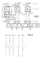
- AD n-1 shows three adders AD n-1 , AD n-2 and AD n-3 , each of which has three inputs.
- the first input of AD n-1 is assigned the most significant bit an-1 of an n-digit binary number A shown in two's complement, the first input of AD n-2 with a n-2 and the first input of AD n-3 with a n-3 .
- the first inputs of further adders, not shown, are occupied with the further bits a n-4 to a0.
- second inputs of the individual adders AD i are each occupied with the individual bits b n-1 , b n-2 ...
- the number D is to be understood as an (n-1) digit binary number, which is supplemented by doubling its sign bit to an n-digit number, the sign bits being fed to the third inputs of AD n-1 and AD n-2, respectively will.
- the result of adding A, B and D is indicated according to the "carry save" principle by two separate signals, one by bit at the sum outputs of the adders AD i Tangible subtotal word s n-1 , s n-2 , s n-3 ... s 0 and a carry word c n , c n-1 , c n-2 ... c 1 which can be tapped bit by bit at the carry outputs of AD i .
- Both words are now combined in an adder AS with individual adders AS n-1 , AS n-2 .... AS0 to form the sum word representing the result of A + B + D.
- Such a previously common input assignment of AS could be shown in FIG. 1 by direct connections (not shown there) of the output of AD n-1 emitting bit s n-1 to input 11 and the carry output of AD n- emitting c n-1. 2 with the entrance 21 and illustrated by the assignments of 12, 13 and 22.
- the most significant adder AD n-1 is now followed by a correction element 1 which has three inputs 2 to 4 and which is integrated with the adder AD n-1 in an arrangement AD kn-1 .
- input 2 is assigned c n
- input 3 is s n-1
- input 4 is c n-1
- An output 5 of the correction element 1 is connected to the input 21 of AS, a second output 6 to the input 11 of AS.
- c n and c n-1 are compared with one another. If this shows that c ⁇ n n-1 is applied to the carry bit c n 2 at instead of s n-1 connected through to the output.
- s 1k 1, so that the sum word s 1k , s0 becomes 1, 1 and thus results in a corrected partial sum of -1.
- Both corrected partial sums result at outputs 31, 32 .. a sum word which corresponds to the desired addition result of -3.
- the corrective measures taken by means of the correction element 1 can also be used when adding three or more digit binary numbers A, B and D, since the carry bit c n-2 , which in this case can no longer be neglected, is not included in the corrective measures mentioned had to become.
- Buffer bits 7, 9, 14 ... and 8, 10 ... which are arranged upstream of the inputs 11, 12 ... and 21, 22 ..., allow carry bits and subtotal bits of the adders AD i to be buffered and when they occur a clock pulse together to the adder AS i .
- Such an arrangement can be expanded in such a way that the outputs of registers 7, 9, 14 ... and 8, 10 ... are fed to the first and second inputs of a row of second adders AD i ⁇ , where the outputs of these subordinate registers 7 ⁇ , 9 ⁇ ... and 8 ⁇ , 10 ⁇ ... are connected to the inputs 11, 12 ... and 21, 22 ... of AS.
- the row of second adders can be followed in the same way by rows of third and fourth adders, each with intermediate buffers connected downstream, the buffer store outputs of the last of these adder rows being connected to the inputs of the adder AS given.
- the buffers are clocked in such a way that the subtotals and carry words of a line in question are each transferred together to the next line, the line in question being acted on with the same clock with the subtotals and carry words of the previous line, which belong to a different addition process.
- FIG. 2 shows a function table for the adder AD n-2 without a correction element, which is also valid for the adders Ad o ... AD n-3 .
- the bits a n-2 , b n-2 , d n-2 supplied to the three inputs of this subcircuit are listed first, and in the last two columns the bits c n-1 and s n-2 , which are indicated in inverted form as c n-1 and s n-2 .
- FIG. 3 shows a circuit example of the adder AD n-1 implemented in CMOS technology, which corresponds to the other adders AD o and A Dn-2 in terms of structure and mode of operation and satisfies the function table in accordance with FIG.
- a circuit point P1 is connected to a connection 15, which is connected to a supply voltage V DD, via three transistor circuits each having two sections.
- the first transistor series circuit consists of the P-channel switching transistors T1 and T2, the second of the P-channel switching transistors T1 and T3 and the third of the P-channel switching transistors T4 and T5.
- the gate of T1 can be controlled via the third input of AD n-1 occupied by d n-2 , the gates of T2 and T4 via the second input occupied by b n-1 and the gates of T3 and T5 via the one of a n -1 wired first input.
- P1 is connected via three two-part transistor series circuits to a connection 16 which is connected to the reference potential. These series circuits T6 and T7, T6 and T8 as well as T9 and T10 are each made up of N-channel field effect transistors.
- the gate of T6 is driven with d n-2 , the gates of T7 and T9 with b n-1 and the gates of T8 and T10 with a n-1 .
- the circuit point P1 corresponds to a carry output AGC from AD n-1 , at which the inverted carry signal c n ⁇ can be tapped.
- Another switching point P2 is connected to the connection via three P-channel switching transistors T11 to T13, a third switching point P3 is connected to connection 16 via three N-channel switching transistors T14 to T16.
- T11 and T14 are each connected via d n- 2 controllable, T12 and T15 each via b n-1 and T13 and T16 each via a n-1 .
- the circuit points P2 and P3 are via the series connection of a P-channel switching transistor T17 and an N-channel switching transistor T18 are connected to one another, the gates of T17 and T18 being connected to P1, while the connection point of T17 and T18 represents an output AGS of AD n-1 at which the inverted sum bit s n-1 ⁇ occurs.
- This latter output is also connected via a three-part series connection of P-channel switching transistors T19 to T21 and via a three-part series connection of N-channel switching transistors T22 to T24 to node 16.
- the gates of T19 and T22 are d n -2 controllable, the gates of T20 and T23 with b n-1 and the gates of T21 and T24 with a n-1 .
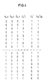
- FIG. 4 shows a function table for the most significant adders AD n-1 and the integrated correction element 1.
- the bits a n-1 , b n-1 , d n-1 and c n-1 fed to the four inputs of this subcircuit are initially listed, but the latter in inverted form c n-1 , and in the last two columns then in each case the bits c n and s (n-1) k that occur as a function thereof at the outputs 5 and 6, these likewise being indicated in inverted form as c n ⁇ and s (n-1) k ⁇ .
- FIG. 5 shows a circuit example implemented in CMOS technology of the subcircuit consisting of AD n-1 and the correction element 1, which is sufficient for the function table according to FIG. 4.
- This subcircuit results from slight changes or expansions from the circuit according to FIG. 3.
- the AGC output is still connected to point P1.
- the gates of the switching transistors T17 and T18 are not driven via point P1 but with the inverted transmission bit c n-1 ⁇ .
Landscapes
- Engineering & Computer Science (AREA)
- Physics & Mathematics (AREA)
- General Physics & Mathematics (AREA)
- Theoretical Computer Science (AREA)
- Pure & Applied Mathematics (AREA)
- Mathematical Analysis (AREA)
- Computational Mathematics (AREA)
- Computing Systems (AREA)
- Mathematical Optimization (AREA)
- General Engineering & Computer Science (AREA)
- Complex Calculations (AREA)
- Compression, Expansion, Code Conversion, And Decoders (AREA)
- Analogue/Digital Conversion (AREA)
- Processing Of Color Television Signals (AREA)
- Transmission Systems Not Characterized By The Medium Used For Transmission (AREA)
Priority Applications (1)
| Application Number | Priority Date | Filing Date | Title |
|---|---|---|---|
| AT87107981T ATE93635T1 (de) | 1986-06-10 | 1987-06-02 | Anordnung zur bitparallelen addition von binaerzahlen mit carry-save ueberlaufkorrektur. |
Applications Claiming Priority (2)
| Application Number | Priority Date | Filing Date | Title |
|---|---|---|---|
| DE3619437 | 1986-06-10 | ||
| DE3619437 | 1986-06-10 |
Publications (3)
| Publication Number | Publication Date |
|---|---|
| EP0249132A2 true EP0249132A2 (fr) | 1987-12-16 |
| EP0249132A3 EP0249132A3 (en) | 1990-05-30 |
| EP0249132B1 EP0249132B1 (fr) | 1993-08-25 |
Family
ID=6302659
Family Applications (1)
| Application Number | Title | Priority Date | Filing Date |
|---|---|---|---|
| EP87107981A Expired - Lifetime EP0249132B1 (fr) | 1986-06-10 | 1987-06-02 | Montage pour l'addition de bits en parallèle de nombre binaires avec correction de débordement par sauvegarde des retenues |
Country Status (5)
| Country | Link |
|---|---|
| US (1) | US4888723A (fr) |
| EP (1) | EP0249132B1 (fr) |
| JP (1) | JPH0724014B2 (fr) |
| AT (1) | ATE93635T1 (fr) |
| DE (1) | DE3787123D1 (fr) |
Families Citing this family (2)
| Publication number | Priority date | Publication date | Assignee | Title |
|---|---|---|---|---|
| JPH0391832A (ja) * | 1989-09-05 | 1991-04-17 | Sony Corp | 加算回路 |
| US5351207A (en) * | 1992-08-31 | 1994-09-27 | Intel Corporation | Methods and apparatus for subtraction with 3:2 carry-save adders |
Family Cites Families (3)
| Publication number | Priority date | Publication date | Assignee | Title |
|---|---|---|---|---|
| US4110832A (en) * | 1977-04-28 | 1978-08-29 | International Business Machines Corporation | Carry save adder |
| DE3524797A1 (de) * | 1985-07-11 | 1987-01-22 | Siemens Ag | Anordnung zur bitparallelen addition von binaerzahlen |
| DE3524981A1 (de) * | 1985-07-12 | 1987-01-22 | Siemens Ag | Anordnung mit einem saettigbaren carry-save-addierer |
-
1987
- 1987-06-02 AT AT87107981T patent/ATE93635T1/de not_active IP Right Cessation
- 1987-06-02 DE DE87107981T patent/DE3787123D1/de not_active Expired - Fee Related
- 1987-06-02 EP EP87107981A patent/EP0249132B1/fr not_active Expired - Lifetime
- 1987-06-05 JP JP62142129A patent/JPH0724014B2/ja not_active Expired - Lifetime
- 1987-06-10 US US07/060,169 patent/US4888723A/en not_active Expired - Fee Related
Also Published As
| Publication number | Publication date |
|---|---|
| JPH0724014B2 (ja) | 1995-03-15 |
| DE3787123D1 (de) | 1993-09-30 |
| ATE93635T1 (de) | 1993-09-15 |
| EP0249132A3 (en) | 1990-05-30 |
| EP0249132B1 (fr) | 1993-08-25 |
| US4888723A (en) | 1989-12-19 |
| JPS62290928A (ja) | 1987-12-17 |
Similar Documents
| Publication | Publication Date | Title |
|---|---|---|
| DE4302898C2 (de) | Arithmetische Recheneinheit mit Akkumulierfunktion | |
| EP0086904B1 (fr) | Circuit digital de calcul en parallèle pour des nombres binaires positifs et négatifs | |
| EP0209014B1 (fr) | Dispositif ayant un additionneur à réservation de retenue saturable | |
| DE2607042A1 (de) | Spannungs-auswahlschaltung | |
| EP0176981B1 (fr) | Convertisseur numérique-analogique | |
| DE68927560T2 (de) | Hochgeschwindige, hochleistende Nulldetektorschaltung mit Parallelverarbeitung | |
| EP0208275B1 (fr) | Dispositif d'addition parallèle par bit de nombres binaires | |
| DE3940897C2 (de) | Schaltungsanordnung und Verfahren zur Berechnung digitaler Summen in einem Halbleiteraddierer mit Parallelübertrag | |
| EP0051079A1 (fr) | Additionneur/soustracteur binaire parallèle en technique MOS à propagation des retenues et étage d'addition/soustraction approprié | |
| EP0249132B1 (fr) | Montage pour l'addition de bits en parallèle de nombre binaires avec correction de débordement par sauvegarde des retenues | |
| EP0257362A1 (fr) | Additionneur | |
| EP0052157A1 (fr) | Additionneur binaire parallèle en technique MOS à prévision des retenues | |
| EP0086851A1 (fr) | Détecteur de débordement pour circuits additionneurs algébriques | |
| DE3880825T2 (de) | Anordnung zur schnellen addition von binärzahlen. | |
| DE2017132A1 (de) | Binarer Parallel Addierer | |
| DE2623374A1 (de) | Digitale multipliziereinrichtung | |
| EP0333884B1 (fr) | Circuit multiplieur parallèle-série ainsi que ses étages de multiplication et d'addition | |
| EP0088135B1 (fr) | Circuit à transistors à effet de champ, à porte isolée, pour un système un parmi n | |
| DE69622486T2 (de) | Übertragvorgriffsgerät mit alternierender polarität | |
| DE69026363T2 (de) | Multipositionsverschieber mit Paritätsbitgenerator | |
| DE1109422B (de) | Asynchrone binaere Additions- und Subtraktionseinrichtung | |
| DE69222054T2 (de) | Einzelbitaddierer | |
| EP0106000A1 (fr) | Circuit digital de suppression des changements d'un signal digital | |
| EP0433315A1 (fr) | Circuits d'addition ou de soustraction d'operandes codes selon un code bcd ou dual | |
| DE3339985A1 (de) | Schaltungsanordnung zur zaehlung von 1-belegungen in (0,1)-vektoren |
Legal Events
| Date | Code | Title | Description |
|---|---|---|---|
| PUAI | Public reference made under article 153(3) epc to a published international application that has entered the european phase |
Free format text: ORIGINAL CODE: 0009012 |
|
| AK | Designated contracting states |
Kind code of ref document: A2 Designated state(s): AT CH DE FR GB IT LI |
|
| PUAL | Search report despatched |
Free format text: ORIGINAL CODE: 0009013 |
|
| AK | Designated contracting states |
Kind code of ref document: A3 Designated state(s): AT CH DE FR GB IT LI |
|
| 17P | Request for examination filed |
Effective date: 19900625 |
|
| 17Q | First examination report despatched |
Effective date: 19911114 |
|
| GRAA | (expected) grant |
Free format text: ORIGINAL CODE: 0009210 |
|
| AK | Designated contracting states |
Kind code of ref document: B1 Designated state(s): AT CH DE FR GB IT LI |
|
| REF | Corresponds to: |
Ref document number: 93635 Country of ref document: AT Date of ref document: 19930915 Kind code of ref document: T |
|
| REF | Corresponds to: |
Ref document number: 3787123 Country of ref document: DE Date of ref document: 19930930 |
|
| ITF | It: translation for a ep patent filed | ||
| GBT | Gb: translation of ep patent filed (gb section 77(6)(a)/1977) |
Effective date: 19931109 |
|
| ET | Fr: translation filed | ||
| PLBE | No opposition filed within time limit |
Free format text: ORIGINAL CODE: 0009261 |
|
| STAA | Information on the status of an ep patent application or granted ep patent |
Free format text: STATUS: NO OPPOSITION FILED WITHIN TIME LIMIT |
|
| 26N | No opposition filed | ||
| PGFP | Annual fee paid to national office [announced via postgrant information from national office to epo] |
Ref country code: GB Payment date: 19950518 Year of fee payment: 9 |
|
| PG25 | Lapsed in a contracting state [announced via postgrant information from national office to epo] |
Ref country code: GB Effective date: 19960602 |
|
| GBPC | Gb: european patent ceased through non-payment of renewal fee |
Effective date: 19960602 |
|
| PGFP | Annual fee paid to national office [announced via postgrant information from national office to epo] |
Ref country code: FR Payment date: 19970626 Year of fee payment: 11 |
|
| PGFP | Annual fee paid to national office [announced via postgrant information from national office to epo] |
Ref country code: CH Payment date: 19971028 Year of fee payment: 11 |
|
| PGFP | Annual fee paid to national office [announced via postgrant information from national office to epo] |
Ref country code: AT Payment date: 19980604 Year of fee payment: 12 |
|
| PG25 | Lapsed in a contracting state [announced via postgrant information from national office to epo] |
Ref country code: LI Free format text: LAPSE BECAUSE OF NON-PAYMENT OF DUE FEES Effective date: 19980630 Ref country code: CH Free format text: LAPSE BECAUSE OF NON-PAYMENT OF DUE FEES Effective date: 19980630 |
|
| PGFP | Annual fee paid to national office [announced via postgrant information from national office to epo] |
Ref country code: DE Payment date: 19980819 Year of fee payment: 12 |
|
| REG | Reference to a national code |
Ref country code: CH Ref legal event code: PL |
|
| PG25 | Lapsed in a contracting state [announced via postgrant information from national office to epo] |
Ref country code: FR Free format text: LAPSE BECAUSE OF NON-PAYMENT OF DUE FEES Effective date: 19990226 |
|
| REG | Reference to a national code |
Ref country code: FR Ref legal event code: ST |
|
| PG25 | Lapsed in a contracting state [announced via postgrant information from national office to epo] |
Ref country code: AT Free format text: LAPSE BECAUSE OF NON-PAYMENT OF DUE FEES Effective date: 19990602 |
|
| PG25 | Lapsed in a contracting state [announced via postgrant information from national office to epo] |
Ref country code: DE Free format text: LAPSE BECAUSE OF NON-PAYMENT OF DUE FEES Effective date: 20000503 |
|
| PG25 | Lapsed in a contracting state [announced via postgrant information from national office to epo] |
Ref country code: IT Free format text: LAPSE BECAUSE OF NON-PAYMENT OF DUE FEES;WARNING: LAPSES OF ITALIAN PATENTS WITH EFFECTIVE DATE BEFORE 2007 MAY HAVE OCCURRED AT ANY TIME BEFORE 2007. THE CORRECT EFFECTIVE DATE MAY BE DIFFERENT FROM THE ONE RECORDED. Effective date: 20050602 |