EP0249371B1 - Dispositif semi-conducteur comprenant deux semi-conducteurs composés et sa méthode de fabrication - Google Patents
Dispositif semi-conducteur comprenant deux semi-conducteurs composés et sa méthode de fabrication Download PDFInfo
- Publication number
- EP0249371B1 EP0249371B1 EP87304812A EP87304812A EP0249371B1 EP 0249371 B1 EP0249371 B1 EP 0249371B1 EP 87304812 A EP87304812 A EP 87304812A EP 87304812 A EP87304812 A EP 87304812A EP 0249371 B1 EP0249371 B1 EP 0249371B1
- Authority
- EP
- European Patent Office
- Prior art keywords
- compound semiconductor
- layer
- impurity
- semiconductor
- semiconductor region
- Prior art date
- Legal status (The legal status is an assumption and is not a legal conclusion. Google has not performed a legal analysis and makes no representation as to the accuracy of the status listed.)
- Expired - Lifetime
Links
Images

Classifications
-
- H—ELECTRICITY
- H10—SEMICONDUCTOR DEVICES; ELECTRIC SOLID-STATE DEVICES NOT OTHERWISE PROVIDED FOR
- H10D—INORGANIC ELECTRIC SEMICONDUCTOR DEVICES
- H10D62/00—Semiconductor bodies, or regions thereof, of devices having potential barriers
- H10D62/80—Semiconductor bodies, or regions thereof, of devices having potential barriers characterised by the materials
- H10D62/82—Heterojunctions
- H10D62/824—Heterojunctions comprising only Group III-V materials heterojunctions, e.g. GaN/AlGaN heterojunctions
-
- H—ELECTRICITY
- H10—SEMICONDUCTOR DEVICES; ELECTRIC SOLID-STATE DEVICES NOT OTHERWISE PROVIDED FOR
- H10D—INORGANIC ELECTRIC SEMICONDUCTOR DEVICES
- H10D62/00—Semiconductor bodies, or regions thereof, of devices having potential barriers
- H10D62/60—Impurity distributions or concentrations
- H10D62/605—Planar doped, e.g. atomic-plane doped or delta-doped
-
- H—ELECTRICITY
- H10—SEMICONDUCTOR DEVICES; ELECTRIC SOLID-STATE DEVICES NOT OTHERWISE PROVIDED FOR
- H10D—INORGANIC ELECTRIC SEMICONDUCTOR DEVICES
- H10D64/00—Electrodes of devices having potential barriers
- H10D64/60—Electrodes characterised by their materials
- H10D64/602—Heterojunction gate electrodes for FETs
-
- H—ELECTRICITY
- H10—SEMICONDUCTOR DEVICES; ELECTRIC SOLID-STATE DEVICES NOT OTHERWISE PROVIDED FOR
- H10P—GENERIC PROCESSES OR APPARATUS FOR THE MANUFACTURE OR TREATMENT OF DEVICES COVERED BY CLASS H10
- H10P14/00—Formation of materials, e.g. in the shape of layers or pillars
- H10P14/20—Formation of materials, e.g. in the shape of layers or pillars of semiconductor materials
- H10P14/29—Formation of materials, e.g. in the shape of layers or pillars of semiconductor materials characterised by the substrates
- H10P14/2901—Materials
- H10P14/2907—Materials being Group IIIA-VA materials
- H10P14/2909—Phosphides
-
- H—ELECTRICITY
- H10—SEMICONDUCTOR DEVICES; ELECTRIC SOLID-STATE DEVICES NOT OTHERWISE PROVIDED FOR
- H10P—GENERIC PROCESSES OR APPARATUS FOR THE MANUFACTURE OR TREATMENT OF DEVICES COVERED BY CLASS H10
- H10P14/00—Formation of materials, e.g. in the shape of layers or pillars
- H10P14/20—Formation of materials, e.g. in the shape of layers or pillars of semiconductor materials
- H10P14/29—Formation of materials, e.g. in the shape of layers or pillars of semiconductor materials characterised by the substrates
- H10P14/2901—Materials
- H10P14/2907—Materials being Group IIIA-VA materials
- H10P14/2911—Arsenides
-
- H—ELECTRICITY
- H10—SEMICONDUCTOR DEVICES; ELECTRIC SOLID-STATE DEVICES NOT OTHERWISE PROVIDED FOR
- H10P—GENERIC PROCESSES OR APPARATUS FOR THE MANUFACTURE OR TREATMENT OF DEVICES COVERED BY CLASS H10
- H10P14/00—Formation of materials, e.g. in the shape of layers or pillars
- H10P14/20—Formation of materials, e.g. in the shape of layers or pillars of semiconductor materials
- H10P14/32—Formation of materials, e.g. in the shape of layers or pillars of semiconductor materials characterised by intermediate layers between substrates and deposited layers
- H10P14/3202—Materials thereof
- H10P14/3214—Materials thereof being Group IIIA-VA semiconductors
- H10P14/3218—Phosphides
-
- H—ELECTRICITY
- H10—SEMICONDUCTOR DEVICES; ELECTRIC SOLID-STATE DEVICES NOT OTHERWISE PROVIDED FOR
- H10P—GENERIC PROCESSES OR APPARATUS FOR THE MANUFACTURE OR TREATMENT OF DEVICES COVERED BY CLASS H10
- H10P14/00—Formation of materials, e.g. in the shape of layers or pillars
- H10P14/20—Formation of materials, e.g. in the shape of layers or pillars of semiconductor materials
- H10P14/32—Formation of materials, e.g. in the shape of layers or pillars of semiconductor materials characterised by intermediate layers between substrates and deposited layers
- H10P14/3202—Materials thereof
- H10P14/3214—Materials thereof being Group IIIA-VA semiconductors
- H10P14/3221—Arsenides
-
- H—ELECTRICITY
- H10—SEMICONDUCTOR DEVICES; ELECTRIC SOLID-STATE DEVICES NOT OTHERWISE PROVIDED FOR
- H10P—GENERIC PROCESSES OR APPARATUS FOR THE MANUFACTURE OR TREATMENT OF DEVICES COVERED BY CLASS H10
- H10P14/00—Formation of materials, e.g. in the shape of layers or pillars
- H10P14/20—Formation of materials, e.g. in the shape of layers or pillars of semiconductor materials
- H10P14/34—Deposited materials, e.g. layers
- H10P14/3402—Deposited materials, e.g. layers characterised by the chemical composition
- H10P14/3414—Deposited materials, e.g. layers characterised by the chemical composition being group IIIA-VIA materials
- H10P14/3418—Phosphides
-
- H—ELECTRICITY
- H10—SEMICONDUCTOR DEVICES; ELECTRIC SOLID-STATE DEVICES NOT OTHERWISE PROVIDED FOR
- H10P—GENERIC PROCESSES OR APPARATUS FOR THE MANUFACTURE OR TREATMENT OF DEVICES COVERED BY CLASS H10
- H10P14/00—Formation of materials, e.g. in the shape of layers or pillars
- H10P14/20—Formation of materials, e.g. in the shape of layers or pillars of semiconductor materials
- H10P14/34—Deposited materials, e.g. layers
- H10P14/3402—Deposited materials, e.g. layers characterised by the chemical composition
- H10P14/3414—Deposited materials, e.g. layers characterised by the chemical composition being group IIIA-VIA materials
- H10P14/3421—Arsenides
-
- H—ELECTRICITY
- H10—SEMICONDUCTOR DEVICES; ELECTRIC SOLID-STATE DEVICES NOT OTHERWISE PROVIDED FOR
- H10P—GENERIC PROCESSES OR APPARATUS FOR THE MANUFACTURE OR TREATMENT OF DEVICES COVERED BY CLASS H10
- H10P14/00—Formation of materials, e.g. in the shape of layers or pillars
- H10P14/20—Formation of materials, e.g. in the shape of layers or pillars of semiconductor materials
- H10P14/34—Deposited materials, e.g. layers
- H10P14/3402—Deposited materials, e.g. layers characterised by the chemical composition
- H10P14/3414—Deposited materials, e.g. layers characterised by the chemical composition being group IIIA-VIA materials
- H10P14/3422—Antimonides
-
- H—ELECTRICITY
- H10—SEMICONDUCTOR DEVICES; ELECTRIC SOLID-STATE DEVICES NOT OTHERWISE PROVIDED FOR
- H10P—GENERIC PROCESSES OR APPARATUS FOR THE MANUFACTURE OR TREATMENT OF DEVICES COVERED BY CLASS H10
- H10P14/00—Formation of materials, e.g. in the shape of layers or pillars
- H10P14/20—Formation of materials, e.g. in the shape of layers or pillars of semiconductor materials
- H10P14/34—Deposited materials, e.g. layers
- H10P14/3438—Doping during depositing
- H10P14/3441—Conductivity type
- H10P14/3442—N-type
-
- H—ELECTRICITY
- H10—SEMICONDUCTOR DEVICES; ELECTRIC SOLID-STATE DEVICES NOT OTHERWISE PROVIDED FOR
- H10P—GENERIC PROCESSES OR APPARATUS FOR THE MANUFACTURE OR TREATMENT OF DEVICES COVERED BY CLASS H10
- H10P14/00—Formation of materials, e.g. in the shape of layers or pillars
- H10P14/20—Formation of materials, e.g. in the shape of layers or pillars of semiconductor materials
- H10P14/34—Deposited materials, e.g. layers
- H10P14/3438—Doping during depositing
- H10P14/3441—Conductivity type
- H10P14/3444—P-type
Definitions
- the present invention relates to a semiconductor device including two compound semiconductors, and a method of manufacturing such a device.
- In x Ga 1-x As y P 1-y mixed crystals which are lattice-matched to InP substrates, especially (InGa)As ternary mixed crystals, exhibit high mobilities such as e.g. 8000 cm 2 /V-sec at room temperature. Therefore, such mixed crystals have been considered as materials for forming high-speed FETs. Since a suitable Schottky junction cannot be formed, a method has been employed wherein a semiconductor device is formed by growing lattice-matched (InAl)As on the surface of the mixed crystals so as to form a Schottky junction on the grown layer (refer to H. Ohno et al: IEEE, Electron Device Lett. Vol. EDL-1, p.154, 1980).
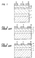
- Such a semiconductor device is shown in Fig. 2 of the accompanying drawings.
- the device has a buffer layer 2 on a substrate, a compound semiconductor layer 3 on the buffer layer 2, and a cap layer 4 of lattice matched InAlAs on the compound semiconductor layer 3.
- Source and drain electrodes 61,62 and a gate electrode 5 are formed on the cap layer 4.
- InAlAs has two disadvantages. It is very prone to oxidation because the mol ratio of AlAs is 0.5, and also it exhibits a Schottky barrier of 0.6 V which is not very high.
- a FET has recently been fabricated experimentally which, as shown in Fig. 3 of the accompanying drawings, has a thin film of GaAs (41) having a lattice constant greatly different from that of an InP substrate (1) is grown on InGaAs layer (3).
- the device shown in Fig. 3 is otherwise similar to that shown in Fig. 2 and corresponding parts are indicated by the same reference numerals.
- a thick film of or above approximately 40 nm cannot afford a good surface because of lattice mismatching which is as much as 4%.
- the leakage current flows through the dislocations, and characteristics satisfactory for the gate electrode of a FET has not been obtained (refer to C.Y. Chen et al: Appl. Phys. Lett., Vol, 46 (1985), p. 1145, and C.Y. Chen et al: IEEE, Electron Device Lett., Vol. EDL-6 (1985), p. 20).
- the present invention seeks to solve, or at least reduce, the problems of the prior art devices discussed above.
- a semiconductor device having a first and a second compound semiconductor regions with a different lattice constants the second compound semiconductor region having at least two semiconductor layers and one impurity layer between these two semiconductor layers.
- the disclosure of this document corresponds to the pre-characterising part of claim 1 of this application.
- a semiconductor device having a first compound semiconductor region (3) with a first lattice constant, and a second compound semiconductor region (41,42,43) on the first compound semiconductor region (3), with a second lattice constant different from the first lattice constant; the second compound semiconductor region (41,42,43) having at least two second compound semiconductor layers (41,43) and there being at least one impurity layer (42) between adjacent second compound semiconductor layers (41,43) of the second compound semiconductor region (41,42,43) respectively; characterized in that:
- the present invention also provides a semiconductor device which has advantages in the fabrication thereof, particularly in that it becomes possible to reduce a device with a very small number of defects.
- a semiconductor device according to the present invention may operate in a stable manner and may have significantly enhanced characteristics.
- a method of manufacturing a semiconductor device comprising forming a first semiconductor layer (41) on a first compound semiconductor region (3) which has a first lattice constant, the first semiconductor layer (41) being a second compound semiconductor with a second lattice constant different from the first lattice constant; forming at least one impurity layer (42) on the first compound semiconductor layer (41); and forming a second semiconductor layer (43) of the second compound semiconductor over the at least one impurity layer (42); characterized in that: the first and second lattice constants differ such that the mismatch thereof causes dislocation networks in the first semiconductor layer (4); and the at least one impurity layer (42) has impurities which are selectively adsorbed or gettered around the dislocations and of such type that they neutralize the resulting charges of the dislocation cores; and in that the impurity concentration in the at least one impurity layer (42) is adapted to the thickness of the second compound semiconductor layers (41,43) such that tunnel currents through the
- first GaAs 41 is grown on an InGaAs layer 3, the GaAs 41 being grown to a thickness of 5 to 30 nm, before growth is suspended.
- a donor impurity 42 such as Si, is adsorbed on the grown surface.
- the growth of further GaAs 43 is restarted, and that growth is stopped at a thickness of at most about 60 nm, being the limit at which the surface morphology of a film deteriorates.
- the thickness is about 40 nm.
- Fig. 5(a) depicts the bending of energy band of GaAs due to a defect caused by a dislocation, so that current tends to flow along the dislocation, i.e. perpendicularly to the plane of the drawing.
- a deep acceptor level 11 induced by a defect such as a dislocation
- holes 21 accumulated by the bending of the energy band in the vicinity of the dislocation.
- the broken line in the figure denotes the Fermi level E f .
- Fig. 5(b) depicts the band gap of GaAs in the semiconductor device according to the present invention.
- a deep acceptor level 11 caused by a defect such as a dislocation.
- the energy band of GaAs is not distorted so much as in Fig. 5(a).
- the GaAs layer is doped with an impurity such as Si. Therefore a donor level 31 based on the doping is formed.
- an impurity such as Si is adsorbed to the dislocation by doping, thereby causing charge neutralization and the suppression of bending of the band. In this example, therefore, holes are not accumulated, and the leakage current decreases significantly.
- the only donor impurity discussed is Si
- another group-IV element for example, Ge or C
- a group-VI element such as S, Se or Te can be used.
- the only grown film, discussed above is of GaAs (the Schottky barrier height of which is about 0.8 eV), but Al z Ga 1-z As which has a higher Schottky barrier may alternatively be used.
- Al z Ga 1-z As when 0 ⁇ z ⁇ 0.5, the barrier height can be increased continuously from 0.8 eV to 1.2 eV.
- the mol ratio of AlAs exceeds 0.7, there is a risk of surface oxidation, as in the case of InAlAs in Fig. 2. Therefore, a mixing ratio of approximately 0 ⁇ z ⁇ 0.5 is more desirable when considering processes for the prevention of oxidation, etc. and also when considering the reliability of the device.
- a method of doping in which, after the suspension of the growth of the film, impurity is adsorbed or ion-implanted into the grown surface, and then the impurity is buried by regrowth, shall be referred to as "atomic layer doping".
- the method of atomic layer doping does not act merely as a doping method, but that it works as passivation for inactivating the high-density dislocation networks existing in the compound semiconductor film. Suspension of the growth of that film may only be performed once, but repetition thereof with growth of each 10 nm of film is more effective. However, when the impurity concentration becomes too high, the apparent height of the Schottky barrier decreases due to the doping effect, and hence, it is more advantageous to form the thickest possible undoped region adjacent the Schottky electrode.
- FIGs. 4(a) and 4(b) are diagrams showing the increase of the leakage current when the impurity doping is excessive.
- Fig. 4(a) depicts the energy band structure of a semiconductor device when an appropriate amount of impurity has been introduced by atomic layer doping.
- a deep level 72 caused by a dislocation or similar defect.
- impurities are introduced by doping in order to reduce the distortion of the band due to the deep level.
- Region 71 is the donor level of the impurity.
- the impurity doping does not affect significantly the height of the Schottky barrier and poses no problem.
- Fig. 4(b) depicts the energy band structure when the amount of the atomic layer doping with impurity is excessive.
- the energy band of a strained cap layer is bent downwards greatly, and tunnel currents 74 due to carriers (electrons) 73 increase, causing leakage current.
- the shape of the potential becomes triangular, so the thickness of the barrier, in effect, decreases.
- the undoped region is as thick as possible adjacent the Schottky electrode.
- FIG. 1 A semi-insulating Fe-doped InP substrate 1 was etched with a mixture of Br-methanol and sulphuric acid : hydrogen peroxide : water to a ratio of 4 : 1 : 1 (volumetric ratio).
- an undoped InP buffer layer 2 was grown to a thickness of about 300 nm
- an n-doped InGaAs layer 3 (the dopant concentration being of the order of 1 x 10 17 cm -3 ) was grown to a thickness of 150 nm
- undoped GaAs 41 was grown to a thickness of 10 nm. The growth of the GaAs was then suspended.
- MOCVD metal-organic chemical vapour deposition
- Si was supplied in the form of disilane (Si 2 H 6 ) and was caused to flow at such a rate that an Si layer 42 with, at most, a uniatomic thickness was adsorbed to the surface of the undoped GaAs 41.
- a GaAs layer 43 was grown again until the whole of the GaAs material was about 40 nm thick.
- a source electrode 61 and a drain electrode 62 were formed by ohmic contact electrodes of AnGe/Ni/An, and a gate electrode 5 was formed by a Schottky electrode of Al/Ti. The static characteristics of the FET thus manufactured were measured.
- n-GaAs (the dopant concentration being of the order of 1 x 10 17 cm -3 and being about 150 nm thick) was grown on semi-insulating GaAs by MOCVD, and an FET was manufactured by the same processes. It was found that the leakage current perforamce of the gate of both the FETs was substantially the same.
- an InGaAs-based MESFET equivalent to a MESFET of GaAs can be produced according to the method of the present invention.
- the growth was carried out with the growth temperature lowered from 640 °C to 600 °C and 550 °C, to form devices of the structure in Fig. 1, and the characteristics of the devices were compared. It was found that, at the lower growth temperature, the FET was improved, as the leakage current of the gate was reduced.
- a sample device grown as in Fig. 1 was produced by molecular beam epitaxy (MBE) and favourable FET characteristics with a reduced leakage current were attained.
- MBE molecular beam epitaxy
- InAlAs lattice-matched with InP instead of InP, similar favourable characteristics were attained.
- the method of the present invention is similarly applicable to any situation where a thin layer of a material of higher Schottky barrier, such as GaAs, is grown on a material of lower Schottky barrier, for example, InP, InAs, or InSb(InGa)(AsP).
- Ion implantation of Si was also effective as a method of achieving impurity adsorption when the growth of the compound semiconductor was by MBE. On this occasion, growth was suspended, the ions were implanted to shallow depth several tens of nanometres in the surface of the grown layer, and the growth was thereafter restarted.
- the operating layer of a device and a material for forming a Schottky junction need not always be lattice-matched.
- the combination of optimum materials can be used in each case, and there may be enhancement in performance and expansion in the versatility of design of an FET and other devices employing Schottky junctions.
- the idea that defects such as dislocations generated at a high density in a hetero-boundary are passivated by the electron layer doping based on impurity adsorption is important from the viewpoint of improving the reliability of the device.
Landscapes
- Junction Field-Effect Transistors (AREA)
- Recrystallisation Techniques (AREA)
Claims (10)
- Dispositif à semiconducteurs comportant une première région semiconductrice composite (3) possédant une première constante de réseau, et une seconde région semiconductrice composite (41,42,43) située sur la première région semiconductrice composite (3) et possédant une seconde constante de réseau différente de la première constante de réseau;
la seconde région semiconductrice composite (41, 42,43) possédant au moins deux secondes couches semiconductrices composites (41,43), avec au moins une couche d'impuretés (42) disposée respectivement entre des secondes couches semiconductrices composites adjacentes (41,43) de la seconde région semiconductrice composite (41,42,43);
caractérisé en ce que :
les première et seconde constantes de réseau des première et seconde régions semiconductrices composites (3;41,42,43) diffèrent de telle sorte que leur désadaptation de réseau produit des réseaux de dislocation dans les secondes couches semiconductrices composites (41) voisines de la première région semiconductrice composite (3); en ce que la ou les couches d'impuretés (42) comportent des impuretés qui sont adsorbées ou dégazées sélectivement autour des dislocations et sont d'un type tel qu'elles neutralisent les charges résultantes des noyaux de dislocation; et en ce que la concentration en impuretés dans la ou les couches d'impuretés (42) est adaptée à l'épaisseur des secondes couches semiconductrices composites (41,43) de telle sorte que des courants d'effet tunnel à travers la seconde région semiconductrice (41,42,43) sont évités. - Dispositif à semiconducteurs selon la revendication 1, dans lequel les impuretés sont des donneurs.
- Dispositif à semiconducteurs selon la revendication 1 ou 2, dans lequel la couche d'impuretés (42) contient du Si en tant qu'impureté.
- Dispositif à semiconducteurs selon l'une quelconque des revendications précédentes, dans lequel la seconde couche semiconductrice composite (43) de la seconde région semiconductrice composite la plus éloignée du premier semiconducteur composite (3) possède une épaisseur non supérieure à 60 nm, et la ou chaque autre seconde couche semiconductrice composite possède une épaisseur comprise entre 5 et 30 nm.
- Dispositif à semiconducteurs selon l'une quelconque des revendications précédentes, dans lequel la première région semiconductrice composite (3) est formée de (InGa)As.
- Dispositif à semiconducteurs selon l'une quelconque des revendications précédentes, dans lequel la seconde région semiconductrice composite est formée de GaAs.
- Dispositif à semiconducteurs selon l'une quelconque des revendications 1 à 5, dans lequel ladite seconde région semiconductrice composite est formée de Ga1-ZAlZAs (0 < Z ≤ 0,7).
- Dispositif à semiconducteurs selon l'une quelconque des revendications 1 à 4, dans lequel la première région semiconductrice composite est un cristal mixte quaternaire exprimé par (InXGa1-X) (AsYP1-Y) avec 0<X, Y<1; et le second semiconducteur composite est un cristal mixte tertiaire exprimé par Ga1-ZAlZAs avec 0<Z≤0,7.
- Procédé de fabrication d'un dispositif à semiconducteurs consistant à former une première couche semiconductrice (41) sur une première région semiconductrice composite (3), qui possède une première constante de réseau, la première couche semiconductrice (41) étant formée d'un second semiconducteur composite possédant une seconde constante de réseau différente de la première constante de réseau; former au moins une couche d'impuretés (42) sur la première couche semiconductrice composite (41); et
former une seconde couche semiconductrice (43) du second semiconducteur composite sur la ou les couches d'impuretés (42);
caractérisé en ce que :
les première et seconde constantes de réseau diffèrent de telle sorte que leur désadaptation produit des réseaux de dislocation dans la première couche semiconductrice (4); et la ou les couches d'impuretés (42) comportent des impuretés qui sont adsorbées ou dégazées sélectivement autour des dislocations et sont d'un type tel qu'elles neutralisent les charges résultantes des noyaux de dislocation; et en ce que la concentration en impuretés dans la ou les couches d'impuretés (42) est adaptée à l'épaisseur des secondes couches semiconductrices composites (41,43) de telle sorte que des courants d'effet tunnel à travers la seconde région semiconductrice (41,42,43) sont évités. - Procédé selon la revendication 9, dans lequel la première couche semiconductrice (41) et la seconde couche semiconductrice (43) sont formées par croissance cristalline.
Applications Claiming Priority (2)
| Application Number | Priority Date | Filing Date | Title |
|---|---|---|---|
| JP61125736A JPH0783028B2 (ja) | 1986-06-02 | 1986-06-02 | 半導体装置及び製造方法 |
| JP125736/86 | 1986-06-02 |
Publications (3)
| Publication Number | Publication Date |
|---|---|
| EP0249371A2 EP0249371A2 (fr) | 1987-12-16 |
| EP0249371A3 EP0249371A3 (en) | 1988-10-05 |
| EP0249371B1 true EP0249371B1 (fr) | 1996-09-04 |
Family
ID=14917516
Family Applications (1)
| Application Number | Title | Priority Date | Filing Date |
|---|---|---|---|
| EP87304812A Expired - Lifetime EP0249371B1 (fr) | 1986-06-02 | 1987-06-01 | Dispositif semi-conducteur comprenant deux semi-conducteurs composés et sa méthode de fabrication |
Country Status (4)
| Country | Link |
|---|---|
| US (1) | US4814838A (fr) |
| EP (1) | EP0249371B1 (fr) |
| JP (1) | JPH0783028B2 (fr) |
| DE (1) | DE3751892T2 (fr) |
Families Citing this family (13)
| Publication number | Priority date | Publication date | Assignee | Title |
|---|---|---|---|---|
| FR2620268A1 (fr) * | 1987-09-03 | 1989-03-10 | Centre Nat Rech Scient | Procede de dopage d'une couche semi-conductrice et transistor obtenu par ce procede |
| JP2770340B2 (ja) * | 1988-09-06 | 1998-07-02 | ソニー株式会社 | 半導体装置、絶縁ゲート型電界効果トランジスタ及びショットキーゲート型電界効果トランジスタ |
| US6083220A (en) | 1990-03-13 | 2000-07-04 | The Regents Of The University Of California | Endovascular electrolytically detachable wire and tip for the formation of thrombus in arteries, veins, aneurysms, vascular malformations and arteriovenous fistulas |
| USRE42625E1 (en) | 1990-03-13 | 2011-08-16 | The Regents Of The University Of California | Endovascular electrolytically detachable wire and tip for the formation of thrombus in arteries, veins, aneurysms, vascular malformations and arteriovenous fistulas |
| USRE42756E1 (en) | 1990-03-13 | 2011-09-27 | The Regents Of The University Of California | Endovascular electrolytically detachable wire and tip for the formation of thrombus in arteries, veins, aneurysms, vascular malformations and arteriovenous fistulas |
| JP2817995B2 (ja) * | 1990-03-15 | 1998-10-30 | 富士通株式会社 | ▲iii▼―▲v▼族化合物半導体ヘテロ構造基板および▲iii▼―▲v▼族化合物ヘテロ構造半導体装置 |
| JP2549206B2 (ja) * | 1990-12-27 | 1996-10-30 | 住友電気工業株式会社 | 電界効果トランジスタ |
| JPH0521468A (ja) * | 1991-07-17 | 1993-01-29 | Sumitomo Electric Ind Ltd | 電界効果トランジスタの製造方法 |
| JP3224437B2 (ja) * | 1992-11-30 | 2001-10-29 | 富士通株式会社 | Iii−v族化合物半導体装置 |
| JP3376078B2 (ja) * | 1994-03-18 | 2003-02-10 | 富士通株式会社 | 高電子移動度トランジスタ |
| US6043143A (en) * | 1998-05-04 | 2000-03-28 | Motorola, Inc. | Ohmic contact and method of manufacture |
| DE10025264A1 (de) * | 2000-05-22 | 2001-11-29 | Max Planck Gesellschaft | Feldeffekt-Transistor auf der Basis von eingebetteten Clusterstrukturen und Verfahren zu seiner Herstellung |
| US9692209B2 (en) | 2011-06-10 | 2017-06-27 | Massachusetts Institute Of Technology | High-concentration active doping in semiconductors and semiconductor devices produced by such doping |
Family Cites Families (3)
| Publication number | Priority date | Publication date | Assignee | Title |
|---|---|---|---|---|
| US3953876A (en) * | 1973-06-07 | 1976-04-27 | Dow Corning Corporation | Silicon solar cell array |
| US4062038A (en) * | 1976-01-28 | 1977-12-06 | International Business Machines Corporation | Radiation responsive device |
| US4632712A (en) * | 1983-09-12 | 1986-12-30 | Massachusetts Institute Of Technology | Reducing dislocations in semiconductors utilizing repeated thermal cycling during multistage epitaxial growth |
-
1986
- 1986-06-02 JP JP61125736A patent/JPH0783028B2/ja not_active Expired - Lifetime
-
1987
- 1987-06-01 DE DE3751892T patent/DE3751892T2/de not_active Expired - Fee Related
- 1987-06-01 EP EP87304812A patent/EP0249371B1/fr not_active Expired - Lifetime
- 1987-06-02 US US07/056,657 patent/US4814838A/en not_active Expired - Fee Related
Non-Patent Citations (4)
| Title |
|---|
| APPLIED PHYSICS LETTERS, vol. 52, no. 7, 1988, pp. 543-545 ; M. SHINOHARA et al.: "Dislocation-free GaAs epitaxial growth with the use of modulation-doped AIAs-GaAs superlattice buffer layers" * |
| IEEE Journal of Quantum Electronics, vol. QE-11, no. 7, 1975, pp. 562-568 ; P.A. Kirkby : "Dislocation Pinning in GaAs by the Deliberate Introduction of Impurities" * |
| JOURNAL OF APPLIED PHYSICS, vol. 47, no. 7, 1976, pp. 3374-3376 ; Y. SEKI et al.: "Impurity effect on the growth of dislocation-free InP single crystals" * |
| JOURNAL OF APPLIED PHYSICS, vol. 62, no. 7, 1988, pp. 543-545 ; I. YONENAGA et al.: "Effects of In impurity on the dynamic behavior of dislocations in GaAs" * |
Also Published As
| Publication number | Publication date |
|---|---|
| JPH0783028B2 (ja) | 1995-09-06 |
| EP0249371A3 (en) | 1988-10-05 |
| EP0249371A2 (fr) | 1987-12-16 |
| DE3751892T2 (de) | 1997-04-03 |
| JPS62283675A (ja) | 1987-12-09 |
| DE3751892D1 (de) | 1996-10-10 |
| US4814838A (en) | 1989-03-21 |
Similar Documents
| Publication | Publication Date | Title |
|---|---|---|
| EP0447327B1 (fr) | Dispositif semi-conducteur à hétérostructure | |
| JP2801624B2 (ja) | ヘテロ接合バイポーラトランジスタ | |
| US5495115A (en) | Semiconductor crystalline laminate structure, forming method of the same, and semiconductor device employing the same | |
| US5903018A (en) | Bipolar transistor including a compound semiconductor | |
| US5837565A (en) | Semiconductor device | |
| US5521404A (en) | Group III-V interdiffusion prevented hetero-junction semiconductor device | |
| EP0249371B1 (fr) | Dispositif semi-conducteur comprenant deux semi-conducteurs composés et sa méthode de fabrication | |
| EP0381396A1 (fr) | Dispositifs à semi-conducteur composé | |
| US5596211A (en) | Field effect transistor having a graded bandgap InGaAsP channel formed of a two-dimensional electron gas | |
| EP0051271B1 (fr) | Dispositif semiconducteur à hétérojonctions | |
| US5952672A (en) | Semiconductor device and method for fabricating the same | |
| US6919589B2 (en) | HEMT with a graded InGaAlP layer separating ohmic and Schottky contacts | |
| US20020003245A1 (en) | Compound semiconductor device and method of manufacturing the same | |
| US5322808A (en) | Method of fabricating inverted modulation-doped heterostructure | |
| KR920006434B1 (ko) | 공진 터널링 장벽구조장치 | |
| JP2604377B2 (ja) | 共振トンネル装置 | |
| US5381027A (en) | Semiconductor device having a heterojunction and a two dimensional gas as an active layer | |
| US5258631A (en) | Semiconductor device having a two-dimensional electron gas as an active layer | |
| EP0405832A1 (fr) | Procédés de dopage pour composants semi-conducteurs | |
| US6429103B1 (en) | MOCVD-grown emode HIGFET buffer | |
| JPH06163962A (ja) | 太陽電池 | |
| US5206528A (en) | Compound semiconductor field effect transistor having a gate insulator formed of insulative superlattice layer | |
| JP2557373B2 (ja) | 化合物半導体装置 | |
| JP2703885B2 (ja) | 半導体装置 | |
| EP0247667B1 (fr) | Transistors à porteurs de charge chauds |
Legal Events
| Date | Code | Title | Description |
|---|---|---|---|
| PUAI | Public reference made under article 153(3) epc to a published international application that has entered the european phase |
Free format text: ORIGINAL CODE: 0009012 |
|
| 17P | Request for examination filed |
Effective date: 19870714 |
|
| AK | Designated contracting states |
Kind code of ref document: A2 Designated state(s): DE FR GB |
|
| PUAL | Search report despatched |
Free format text: ORIGINAL CODE: 0009013 |
|
| AK | Designated contracting states |
Kind code of ref document: A3 Designated state(s): DE FR GB |
|
| 17Q | First examination report despatched |
Effective date: 19910208 |
|
| GRAG | Despatch of communication of intention to grant |
Free format text: ORIGINAL CODE: EPIDOS AGRA |
|
| GRAH | Despatch of communication of intention to grant a patent |
Free format text: ORIGINAL CODE: EPIDOS IGRA |
|
| GRAH | Despatch of communication of intention to grant a patent |
Free format text: ORIGINAL CODE: EPIDOS IGRA |
|
| GRAA | (expected) grant |
Free format text: ORIGINAL CODE: 0009210 |
|
| AK | Designated contracting states |
Kind code of ref document: B1 Designated state(s): DE FR GB |
|
| REF | Corresponds to: |
Ref document number: 3751892 Country of ref document: DE Date of ref document: 19961010 |
|
| ET | Fr: translation filed | ||
| PLBE | No opposition filed within time limit |
Free format text: ORIGINAL CODE: 0009261 |
|
| STAA | Information on the status of an ep patent application or granted ep patent |
Free format text: STATUS: NO OPPOSITION FILED WITHIN TIME LIMIT |
|
| 26N | No opposition filed | ||
| PGFP | Annual fee paid to national office [announced via postgrant information from national office to epo] |
Ref country code: FR Payment date: 19980320 Year of fee payment: 12 |
|
| PGFP | Annual fee paid to national office [announced via postgrant information from national office to epo] |
Ref country code: GB Payment date: 19980414 Year of fee payment: 12 |
|
| PGFP | Annual fee paid to national office [announced via postgrant information from national office to epo] |
Ref country code: DE Payment date: 19980630 Year of fee payment: 12 |
|
| PG25 | Lapsed in a contracting state [announced via postgrant information from national office to epo] |
Ref country code: GB Free format text: LAPSE BECAUSE OF NON-PAYMENT OF DUE FEES Effective date: 19990601 |
|
| PG25 | Lapsed in a contracting state [announced via postgrant information from national office to epo] |
Ref country code: FR Free format text: THE PATENT HAS BEEN ANNULLED BY A DECISION OF A NATIONAL AUTHORITY Effective date: 19990630 |
|
| GBPC | Gb: european patent ceased through non-payment of renewal fee |
Effective date: 19990601 |
|
| PG25 | Lapsed in a contracting state [announced via postgrant information from national office to epo] |
Ref country code: DE Free format text: LAPSE BECAUSE OF NON-PAYMENT OF DUE FEES Effective date: 20000503 |
|
| REG | Reference to a national code |
Ref country code: FR Ref legal event code: ST |
|
| APAH | Appeal reference modified |
Free format text: ORIGINAL CODE: EPIDOSCREFNO |