EP0250227A2 - Verfahren zur Herstellung einer Karte mit optischer Aufzeichnung und optisches Aufzeichnungsmedium vom Transfertyp - Google Patents
Verfahren zur Herstellung einer Karte mit optischer Aufzeichnung und optisches Aufzeichnungsmedium vom Transfertyp Download PDFInfo
- Publication number
- EP0250227A2 EP0250227A2 EP87305372A EP87305372A EP0250227A2 EP 0250227 A2 EP0250227 A2 EP 0250227A2 EP 87305372 A EP87305372 A EP 87305372A EP 87305372 A EP87305372 A EP 87305372A EP 0250227 A2 EP0250227 A2 EP 0250227A2
- Authority
- EP
- European Patent Office
- Prior art keywords
- optical recording
- layer
- based resin
- recording medium
- transfer type
- Prior art date
- Legal status (The legal status is an assumption and is not a legal conclusion. Google has not performed a legal analysis and makes no representation as to the accuracy of the status listed.)
- Granted
Links
Images


Classifications
-
- B—PERFORMING OPERATIONS; TRANSPORTING
- B42—BOOKBINDING; ALBUMS; FILES; SPECIAL PRINTED MATTER
- B42D—BOOKS; BOOK COVERS; LOOSE LEAVES; PRINTED MATTER CHARACTERISED BY IDENTIFICATION OR SECURITY FEATURES; PRINTED MATTER OF SPECIAL FORMAT OR STYLE NOT OTHERWISE PROVIDED FOR; DEVICES FOR USE THEREWITH AND NOT OTHERWISE PROVIDED FOR; MOVABLE-STRIP WRITING OR READING APPARATUS
- B42D25/00—Information-bearing cards or sheet-like structures characterised by identification or security features; Manufacture thereof
- B42D25/40—Manufacture
- B42D25/45—Associating two or more layers
- B42D25/465—Associating two or more layers using chemicals or adhesives
- B42D25/47—Associating two or more layers using chemicals or adhesives using adhesives
-
- B—PERFORMING OPERATIONS; TRANSPORTING
- B42—BOOKBINDING; ALBUMS; FILES; SPECIAL PRINTED MATTER
- B42D—BOOKS; BOOK COVERS; LOOSE LEAVES; PRINTED MATTER CHARACTERISED BY IDENTIFICATION OR SECURITY FEATURES; PRINTED MATTER OF SPECIAL FORMAT OR STYLE NOT OTHERWISE PROVIDED FOR; DEVICES FOR USE THEREWITH AND NOT OTHERWISE PROVIDED FOR; MOVABLE-STRIP WRITING OR READING APPARATUS
- B42D25/00—Information-bearing cards or sheet-like structures characterised by identification or security features; Manufacture thereof
- B42D25/40—Manufacture
- B42D25/405—Marking
- B42D25/41—Marking using electromagnetic radiation
-
- B—PERFORMING OPERATIONS; TRANSPORTING
- B42—BOOKBINDING; ALBUMS; FILES; SPECIAL PRINTED MATTER
- B42D—BOOKS; BOOK COVERS; LOOSE LEAVES; PRINTED MATTER CHARACTERISED BY IDENTIFICATION OR SECURITY FEATURES; PRINTED MATTER OF SPECIAL FORMAT OR STYLE NOT OTHERWISE PROVIDED FOR; DEVICES FOR USE THEREWITH AND NOT OTHERWISE PROVIDED FOR; MOVABLE-STRIP WRITING OR READING APPARATUS
- B42D25/00—Information-bearing cards or sheet-like structures characterised by identification or security features; Manufacture thereof
- B42D25/40—Manufacture
- B42D25/45—Associating two or more layers
- B42D25/455—Associating two or more layers using heat
-
- B—PERFORMING OPERATIONS; TRANSPORTING
- B42—BOOKBINDING; ALBUMS; FILES; SPECIAL PRINTED MATTER
- B42D—BOOKS; BOOK COVERS; LOOSE LEAVES; PRINTED MATTER CHARACTERISED BY IDENTIFICATION OR SECURITY FEATURES; PRINTED MATTER OF SPECIAL FORMAT OR STYLE NOT OTHERWISE PROVIDED FOR; DEVICES FOR USE THEREWITH AND NOT OTHERWISE PROVIDED FOR; MOVABLE-STRIP WRITING OR READING APPARATUS
- B42D25/00—Information-bearing cards or sheet-like structures characterised by identification or security features; Manufacture thereof
- B42D25/40—Manufacture
- B42D25/45—Associating two or more layers
- B42D25/46—Associating two or more layers using pressure
-
- G—PHYSICS
- G06—COMPUTING OR CALCULATING; COUNTING
- G06K—GRAPHICAL DATA READING; PRESENTATION OF DATA; RECORD CARRIERS; HANDLING RECORD CARRIERS
- G06K19/00—Record carriers for use with machines and with at least a part designed to carry digital markings
- G06K19/06—Record carriers for use with machines and with at least a part designed to carry digital markings characterised by the kind of the digital marking, e.g. shape, nature, code
- G06K19/06009—Record carriers for use with machines and with at least a part designed to carry digital markings characterised by the kind of the digital marking, e.g. shape, nature, code with optically detectable marking
- G06K19/06046—Constructional details
-
- G—PHYSICS
- G11—INFORMATION STORAGE
- G11B—INFORMATION STORAGE BASED ON RELATIVE MOVEMENT BETWEEN RECORD CARRIER AND TRANSDUCER
- G11B7/00—Recording or reproducing by optical means, e.g. recording using a thermal beam of optical radiation by modifying optical properties or the physical structure, reproducing using an optical beam at lower power by sensing optical properties; Record carriers therefor
- G11B7/24—Record carriers characterised by shape, structure or physical properties, or by the selection of the material
- G11B7/241—Record carriers characterised by shape, structure or physical properties, or by the selection of the material characterised by the selection of the material
- G11B7/242—Record carriers characterised by shape, structure or physical properties, or by the selection of the material characterised by the selection of the material of recording layers
- G11B7/243—Record carriers characterised by shape, structure or physical properties, or by the selection of the material characterised by the selection of the material of recording layers comprising inorganic materials only, e.g. ablative layers
-
- G—PHYSICS
- G11—INFORMATION STORAGE
- G11B—INFORMATION STORAGE BASED ON RELATIVE MOVEMENT BETWEEN RECORD CARRIER AND TRANSDUCER
- G11B7/00—Recording or reproducing by optical means, e.g. recording using a thermal beam of optical radiation by modifying optical properties or the physical structure, reproducing using an optical beam at lower power by sensing optical properties; Record carriers therefor
- G11B7/24—Record carriers characterised by shape, structure or physical properties, or by the selection of the material
- G11B7/241—Record carriers characterised by shape, structure or physical properties, or by the selection of the material characterised by the selection of the material
- G11B7/242—Record carriers characterised by shape, structure or physical properties, or by the selection of the material characterised by the selection of the material of recording layers
- G11B7/244—Record carriers characterised by shape, structure or physical properties, or by the selection of the material characterised by the selection of the material of recording layers comprising organic materials only
-
- G—PHYSICS
- G11—INFORMATION STORAGE
- G11B—INFORMATION STORAGE BASED ON RELATIVE MOVEMENT BETWEEN RECORD CARRIER AND TRANSDUCER
- G11B7/00—Recording or reproducing by optical means, e.g. recording using a thermal beam of optical radiation by modifying optical properties or the physical structure, reproducing using an optical beam at lower power by sensing optical properties; Record carriers therefor
- G11B7/24—Record carriers characterised by shape, structure or physical properties, or by the selection of the material
- G11B7/241—Record carriers characterised by shape, structure or physical properties, or by the selection of the material characterised by the selection of the material
- G11B7/252—Record carriers characterised by shape, structure or physical properties, or by the selection of the material characterised by the selection of the material of layers other than recording layers
- G11B7/256—Record carriers characterised by shape, structure or physical properties, or by the selection of the material characterised by the selection of the material of layers other than recording layers of layers improving adhesion between layers
-
- G—PHYSICS
- G11—INFORMATION STORAGE
- G11B—INFORMATION STORAGE BASED ON RELATIVE MOVEMENT BETWEEN RECORD CARRIER AND TRANSDUCER
- G11B7/00—Recording or reproducing by optical means, e.g. recording using a thermal beam of optical radiation by modifying optical properties or the physical structure, reproducing using an optical beam at lower power by sensing optical properties; Record carriers therefor
- G11B7/24—Record carriers characterised by shape, structure or physical properties, or by the selection of the material
- G11B7/241—Record carriers characterised by shape, structure or physical properties, or by the selection of the material characterised by the selection of the material
- G11B7/252—Record carriers characterised by shape, structure or physical properties, or by the selection of the material characterised by the selection of the material of layers other than recording layers
- G11B7/258—Record carriers characterised by shape, structure or physical properties, or by the selection of the material characterised by the selection of the material of layers other than recording layers of reflective layers
-
- B—PERFORMING OPERATIONS; TRANSPORTING
- B42—BOOKBINDING; ALBUMS; FILES; SPECIAL PRINTED MATTER
- B42D—BOOKS; BOOK COVERS; LOOSE LEAVES; PRINTED MATTER CHARACTERISED BY IDENTIFICATION OR SECURITY FEATURES; PRINTED MATTER OF SPECIAL FORMAT OR STYLE NOT OTHERWISE PROVIDED FOR; DEVICES FOR USE THEREWITH AND NOT OTHERWISE PROVIDED FOR; MOVABLE-STRIP WRITING OR READING APPARATUS
- B42D25/00—Information-bearing cards or sheet-like structures characterised by identification or security features; Manufacture thereof
- B42D25/40—Manufacture
- B42D25/45—Associating two or more layers
-
- G—PHYSICS
- G11—INFORMATION STORAGE
- G11B—INFORMATION STORAGE BASED ON RELATIVE MOVEMENT BETWEEN RECORD CARRIER AND TRANSDUCER
- G11B7/00—Recording or reproducing by optical means, e.g. recording using a thermal beam of optical radiation by modifying optical properties or the physical structure, reproducing using an optical beam at lower power by sensing optical properties; Record carriers therefor
- G11B7/24—Record carriers characterised by shape, structure or physical properties, or by the selection of the material
- G11B7/241—Record carriers characterised by shape, structure or physical properties, or by the selection of the material characterised by the selection of the material
- G11B7/242—Record carriers characterised by shape, structure or physical properties, or by the selection of the material characterised by the selection of the material of recording layers
- G11B7/243—Record carriers characterised by shape, structure or physical properties, or by the selection of the material characterised by the selection of the material of recording layers comprising inorganic materials only, e.g. ablative layers
- G11B2007/24302—Metals or metalloids
- G11B2007/24306—Metals or metalloids transition metal elements of groups 3-10
-
- G—PHYSICS
- G11—INFORMATION STORAGE
- G11B—INFORMATION STORAGE BASED ON RELATIVE MOVEMENT BETWEEN RECORD CARRIER AND TRANSDUCER
- G11B7/00—Recording or reproducing by optical means, e.g. recording using a thermal beam of optical radiation by modifying optical properties or the physical structure, reproducing using an optical beam at lower power by sensing optical properties; Record carriers therefor
- G11B7/24—Record carriers characterised by shape, structure or physical properties, or by the selection of the material
- G11B7/241—Record carriers characterised by shape, structure or physical properties, or by the selection of the material characterised by the selection of the material
- G11B7/242—Record carriers characterised by shape, structure or physical properties, or by the selection of the material characterised by the selection of the material of recording layers
- G11B7/243—Record carriers characterised by shape, structure or physical properties, or by the selection of the material characterised by the selection of the material of recording layers comprising inorganic materials only, e.g. ablative layers
- G11B2007/24302—Metals or metalloids
- G11B2007/24308—Metals or metalloids transition metal elements of group 11 (Cu, Ag, Au)
-
- G—PHYSICS
- G11—INFORMATION STORAGE
- G11B—INFORMATION STORAGE BASED ON RELATIVE MOVEMENT BETWEEN RECORD CARRIER AND TRANSDUCER
- G11B7/00—Recording or reproducing by optical means, e.g. recording using a thermal beam of optical radiation by modifying optical properties or the physical structure, reproducing using an optical beam at lower power by sensing optical properties; Record carriers therefor
- G11B7/24—Record carriers characterised by shape, structure or physical properties, or by the selection of the material
- G11B7/241—Record carriers characterised by shape, structure or physical properties, or by the selection of the material characterised by the selection of the material
- G11B7/242—Record carriers characterised by shape, structure or physical properties, or by the selection of the material characterised by the selection of the material of recording layers
- G11B7/243—Record carriers characterised by shape, structure or physical properties, or by the selection of the material characterised by the selection of the material of recording layers comprising inorganic materials only, e.g. ablative layers
- G11B2007/24302—Metals or metalloids
- G11B2007/2431—Metals or metalloids group 13 elements (B, Al, Ga, In)
-
- G—PHYSICS
- G11—INFORMATION STORAGE
- G11B—INFORMATION STORAGE BASED ON RELATIVE MOVEMENT BETWEEN RECORD CARRIER AND TRANSDUCER
- G11B7/00—Recording or reproducing by optical means, e.g. recording using a thermal beam of optical radiation by modifying optical properties or the physical structure, reproducing using an optical beam at lower power by sensing optical properties; Record carriers therefor
- G11B7/24—Record carriers characterised by shape, structure or physical properties, or by the selection of the material
- G11B7/241—Record carriers characterised by shape, structure or physical properties, or by the selection of the material characterised by the selection of the material
- G11B7/242—Record carriers characterised by shape, structure or physical properties, or by the selection of the material characterised by the selection of the material of recording layers
- G11B7/243—Record carriers characterised by shape, structure or physical properties, or by the selection of the material characterised by the selection of the material of recording layers comprising inorganic materials only, e.g. ablative layers
- G11B2007/24302—Metals or metalloids
- G11B2007/24314—Metals or metalloids group 15 elements (e.g. Sb, Bi)
-
- G—PHYSICS
- G11—INFORMATION STORAGE
- G11B—INFORMATION STORAGE BASED ON RELATIVE MOVEMENT BETWEEN RECORD CARRIER AND TRANSDUCER
- G11B7/00—Recording or reproducing by optical means, e.g. recording using a thermal beam of optical radiation by modifying optical properties or the physical structure, reproducing using an optical beam at lower power by sensing optical properties; Record carriers therefor
- G11B7/24—Record carriers characterised by shape, structure or physical properties, or by the selection of the material
- G11B7/241—Record carriers characterised by shape, structure or physical properties, or by the selection of the material characterised by the selection of the material
- G11B7/242—Record carriers characterised by shape, structure or physical properties, or by the selection of the material characterised by the selection of the material of recording layers
- G11B7/243—Record carriers characterised by shape, structure or physical properties, or by the selection of the material characterised by the selection of the material of recording layers comprising inorganic materials only, e.g. ablative layers
- G11B2007/24302—Metals or metalloids
- G11B2007/24316—Metals or metalloids group 16 elements (i.e. chalcogenides, Se, Te)
-
- G—PHYSICS
- G11—INFORMATION STORAGE
- G11B—INFORMATION STORAGE BASED ON RELATIVE MOVEMENT BETWEEN RECORD CARRIER AND TRANSDUCER
- G11B7/00—Recording or reproducing by optical means, e.g. recording using a thermal beam of optical radiation by modifying optical properties or the physical structure, reproducing using an optical beam at lower power by sensing optical properties; Record carriers therefor
- G11B7/24—Record carriers characterised by shape, structure or physical properties, or by the selection of the material
- G11B7/241—Record carriers characterised by shape, structure or physical properties, or by the selection of the material characterised by the selection of the material
- G11B7/242—Record carriers characterised by shape, structure or physical properties, or by the selection of the material characterised by the selection of the material of recording layers
- G11B7/243—Record carriers characterised by shape, structure or physical properties, or by the selection of the material characterised by the selection of the material of recording layers comprising inorganic materials only, e.g. ablative layers
- G11B2007/24318—Non-metallic elements
- G11B2007/2432—Oxygen
-
- G—PHYSICS
- G11—INFORMATION STORAGE
- G11B—INFORMATION STORAGE BASED ON RELATIVE MOVEMENT BETWEEN RECORD CARRIER AND TRANSDUCER
- G11B7/00—Recording or reproducing by optical means, e.g. recording using a thermal beam of optical radiation by modifying optical properties or the physical structure, reproducing using an optical beam at lower power by sensing optical properties; Record carriers therefor
- G11B7/24—Record carriers characterised by shape, structure or physical properties, or by the selection of the material
- G11B7/241—Record carriers characterised by shape, structure or physical properties, or by the selection of the material characterised by the selection of the material
- G11B7/242—Record carriers characterised by shape, structure or physical properties, or by the selection of the material characterised by the selection of the material of recording layers
- G11B7/243—Record carriers characterised by shape, structure or physical properties, or by the selection of the material characterised by the selection of the material of recording layers comprising inorganic materials only, e.g. ablative layers
- G11B2007/24318—Non-metallic elements
- G11B2007/24328—Carbon
-
- G—PHYSICS
- G11—INFORMATION STORAGE
- G11B—INFORMATION STORAGE BASED ON RELATIVE MOVEMENT BETWEEN RECORD CARRIER AND TRANSDUCER
- G11B7/00—Recording or reproducing by optical means, e.g. recording using a thermal beam of optical radiation by modifying optical properties or the physical structure, reproducing using an optical beam at lower power by sensing optical properties; Record carriers therefor
- G11B7/24—Record carriers characterised by shape, structure or physical properties, or by the selection of the material
- G11B7/241—Record carriers characterised by shape, structure or physical properties, or by the selection of the material characterised by the selection of the material
- G11B7/242—Record carriers characterised by shape, structure or physical properties, or by the selection of the material characterised by the selection of the material of recording layers
- G11B7/244—Record carriers characterised by shape, structure or physical properties, or by the selection of the material characterised by the selection of the material of recording layers comprising organic materials only
- G11B7/245—Record carriers characterised by shape, structure or physical properties, or by the selection of the material characterised by the selection of the material of recording layers comprising organic materials only containing a polymeric component
-
- G—PHYSICS
- G11—INFORMATION STORAGE
- G11B—INFORMATION STORAGE BASED ON RELATIVE MOVEMENT BETWEEN RECORD CARRIER AND TRANSDUCER
- G11B7/00—Recording or reproducing by optical means, e.g. recording using a thermal beam of optical radiation by modifying optical properties or the physical structure, reproducing using an optical beam at lower power by sensing optical properties; Record carriers therefor
- G11B7/24—Record carriers characterised by shape, structure or physical properties, or by the selection of the material
- G11B7/241—Record carriers characterised by shape, structure or physical properties, or by the selection of the material characterised by the selection of the material
- G11B7/242—Record carriers characterised by shape, structure or physical properties, or by the selection of the material characterised by the selection of the material of recording layers
- G11B7/244—Record carriers characterised by shape, structure or physical properties, or by the selection of the material characterised by the selection of the material of recording layers comprising organic materials only
- G11B7/246—Record carriers characterised by shape, structure or physical properties, or by the selection of the material characterised by the selection of the material of recording layers comprising organic materials only containing dyes
- G11B7/248—Record carriers characterised by shape, structure or physical properties, or by the selection of the material characterised by the selection of the material of recording layers comprising organic materials only containing dyes porphines; azaporphines, e.g. phthalocyanines
-
- G—PHYSICS
- G11—INFORMATION STORAGE
- G11B—INFORMATION STORAGE BASED ON RELATIVE MOVEMENT BETWEEN RECORD CARRIER AND TRANSDUCER
- G11B7/00—Recording or reproducing by optical means, e.g. recording using a thermal beam of optical radiation by modifying optical properties or the physical structure, reproducing using an optical beam at lower power by sensing optical properties; Record carriers therefor
- G11B7/24—Record carriers characterised by shape, structure or physical properties, or by the selection of the material
- G11B7/241—Record carriers characterised by shape, structure or physical properties, or by the selection of the material characterised by the selection of the material
- G11B7/252—Record carriers characterised by shape, structure or physical properties, or by the selection of the material characterised by the selection of the material of layers other than recording layers
- G11B7/253—Record carriers characterised by shape, structure or physical properties, or by the selection of the material characterised by the selection of the material of layers other than recording layers of substrates
- G11B7/2533—Record carriers characterised by shape, structure or physical properties, or by the selection of the material characterised by the selection of the material of layers other than recording layers of substrates comprising resins
- G11B7/2534—Record carriers characterised by shape, structure or physical properties, or by the selection of the material characterised by the selection of the material of layers other than recording layers of substrates comprising resins polycarbonates [PC]
-
- G—PHYSICS
- G11—INFORMATION STORAGE
- G11B—INFORMATION STORAGE BASED ON RELATIVE MOVEMENT BETWEEN RECORD CARRIER AND TRANSDUCER
- G11B7/00—Recording or reproducing by optical means, e.g. recording using a thermal beam of optical radiation by modifying optical properties or the physical structure, reproducing using an optical beam at lower power by sensing optical properties; Record carriers therefor
- G11B7/24—Record carriers characterised by shape, structure or physical properties, or by the selection of the material
- G11B7/241—Record carriers characterised by shape, structure or physical properties, or by the selection of the material characterised by the selection of the material
- G11B7/252—Record carriers characterised by shape, structure or physical properties, or by the selection of the material characterised by the selection of the material of layers other than recording layers
- G11B7/254—Record carriers characterised by shape, structure or physical properties, or by the selection of the material characterised by the selection of the material of layers other than recording layers of protective topcoat layers
- G11B7/2542—Record carriers characterised by shape, structure or physical properties, or by the selection of the material characterised by the selection of the material of layers other than recording layers of protective topcoat layers consisting essentially of organic resins
-
- Y—GENERAL TAGGING OF NEW TECHNOLOGICAL DEVELOPMENTS; GENERAL TAGGING OF CROSS-SECTIONAL TECHNOLOGIES SPANNING OVER SEVERAL SECTIONS OF THE IPC; TECHNICAL SUBJECTS COVERED BY FORMER USPC CROSS-REFERENCE ART COLLECTIONS [XRACs] AND DIGESTS
- Y10—TECHNICAL SUBJECTS COVERED BY FORMER USPC
- Y10S—TECHNICAL SUBJECTS COVERED BY FORMER USPC CROSS-REFERENCE ART COLLECTIONS [XRACs] AND DIGESTS
- Y10S428/00—Stock material or miscellaneous articles
- Y10S428/90—Magnetic feature
-
- Y—GENERAL TAGGING OF NEW TECHNOLOGICAL DEVELOPMENTS; GENERAL TAGGING OF CROSS-SECTIONAL TECHNOLOGIES SPANNING OVER SEVERAL SECTIONS OF THE IPC; TECHNICAL SUBJECTS COVERED BY FORMER USPC CROSS-REFERENCE ART COLLECTIONS [XRACs] AND DIGESTS
- Y10—TECHNICAL SUBJECTS COVERED BY FORMER USPC
- Y10S—TECHNICAL SUBJECTS COVERED BY FORMER USPC CROSS-REFERENCE ART COLLECTIONS [XRACs] AND DIGESTS
- Y10S430/00—Radiation imagery chemistry: process, composition, or product thereof
- Y10S430/146—Laser beam
-
- Y—GENERAL TAGGING OF NEW TECHNOLOGICAL DEVELOPMENTS; GENERAL TAGGING OF CROSS-SECTIONAL TECHNOLOGIES SPANNING OVER SEVERAL SECTIONS OF THE IPC; TECHNICAL SUBJECTS COVERED BY FORMER USPC CROSS-REFERENCE ART COLLECTIONS [XRACs] AND DIGESTS
- Y10—TECHNICAL SUBJECTS COVERED BY FORMER USPC
- Y10T—TECHNICAL SUBJECTS COVERED BY FORMER US CLASSIFICATION
- Y10T428/00—Stock material or miscellaneous articles
- Y10T428/28—Web or sheet containing structurally defined element or component and having an adhesive outermost layer
- Y10T428/2804—Next to metal
-
- Y—GENERAL TAGGING OF NEW TECHNOLOGICAL DEVELOPMENTS; GENERAL TAGGING OF CROSS-SECTIONAL TECHNOLOGIES SPANNING OVER SEVERAL SECTIONS OF THE IPC; TECHNICAL SUBJECTS COVERED BY FORMER USPC CROSS-REFERENCE ART COLLECTIONS [XRACs] AND DIGESTS
- Y10—TECHNICAL SUBJECTS COVERED BY FORMER USPC
- Y10T—TECHNICAL SUBJECTS COVERED BY FORMER US CLASSIFICATION
- Y10T428/00—Stock material or miscellaneous articles
- Y10T428/28—Web or sheet containing structurally defined element or component and having an adhesive outermost layer
- Y10T428/2809—Web or sheet containing structurally defined element or component and having an adhesive outermost layer including irradiated or wave energy treated component
-
- Y—GENERAL TAGGING OF NEW TECHNOLOGICAL DEVELOPMENTS; GENERAL TAGGING OF CROSS-SECTIONAL TECHNOLOGIES SPANNING OVER SEVERAL SECTIONS OF THE IPC; TECHNICAL SUBJECTS COVERED BY FORMER USPC CROSS-REFERENCE ART COLLECTIONS [XRACs] AND DIGESTS
- Y10—TECHNICAL SUBJECTS COVERED BY FORMER USPC
- Y10T—TECHNICAL SUBJECTS COVERED BY FORMER US CLASSIFICATION
- Y10T428/00—Stock material or miscellaneous articles
- Y10T428/28—Web or sheet containing structurally defined element or component and having an adhesive outermost layer
- Y10T428/2839—Web or sheet containing structurally defined element or component and having an adhesive outermost layer with release or antistick coating
-
- Y—GENERAL TAGGING OF NEW TECHNOLOGICAL DEVELOPMENTS; GENERAL TAGGING OF CROSS-SECTIONAL TECHNOLOGIES SPANNING OVER SEVERAL SECTIONS OF THE IPC; TECHNICAL SUBJECTS COVERED BY FORMER USPC CROSS-REFERENCE ART COLLECTIONS [XRACs] AND DIGESTS
- Y10—TECHNICAL SUBJECTS COVERED BY FORMER USPC
- Y10T—TECHNICAL SUBJECTS COVERED BY FORMER US CLASSIFICATION
- Y10T428/00—Stock material or miscellaneous articles
- Y10T428/28—Web or sheet containing structurally defined element or component and having an adhesive outermost layer
- Y10T428/2848—Three or more layers
Definitions
- the present invention relates to a method of producing an optical recording card and a transfer type optical recording medium employable for carrying out the method.
- This kind of card is required to record various kinds of informations such as data concerning individual person, data concerning a company from which the card is issued or the like data.
- informations were recorded using visual characters and symbols and in the later age they were recorded in response to electrical signals which were generated magnetically.
- the conventional card is not in position to take adequate measures for preventing data from being falsified and moreover for the current tendency of increased volume of informations.
- optical recording card In view of the current situation as mentioned above a card including an optical recording layer to which the latest optical technology is applied to record informations has been developed in the recent years. This kind of card is called optical recording card.
- a hitherto proposed optical recording card 1 has a basic structure as shown in Figs. 1 and 2. Specifically, it includes an optical recording layer 4 which is interposed between a card base 2 and a transparent protective layer 3 made of transparent plastics and optical reading is carried out from the side of the protective layer 3. It should be noted that in Fig. 2 an adhesive layer is omitted.
- the optical recording layer 4 comprises an optical reflective layer which has optical reflection faces on which a number of data pits are formed. Reading is achieved with the use of laser beam 9 by detecting data pits each of which has a different optical reflectivity.
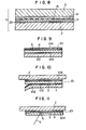
- a transfer type optical recording medium 101 comprises a base film 102, a peeling layer 103, a transparent protective layer 3 made of transparent synthetic resin, an optical recording layer 4 and an adhesive layer 104 which are successively superimposed one above another.
- the base film 102 is peeled off together with the parting layer and a card base 2 is adhesively secured to the transfer type optical recording medium 101 to achieve thermal transfer on necessasry part, as shown in Fig. 10.
- an optical recording card 100 as shown in Fig. 11 is produced.
- a method of producing an optical recording card as mentioned above is a known technique as disclosed in an official gazette of Japanese laid-open patent (official gazette of Japanese Laid-Open Patent No. 58894/1986 issued on the day of April 5, 1985).
- the protective layer 3 of the transfer type optical recording medium 101 used for practicing the above-mentioned prior method of producing a conventional optical recording card constitutes an upper layer of the optical recording card 100 in order to protect the optical recording layer 4 for damage or injury and moreover reduce a rate of occurrence of error during data reading. Accordingly, the protective layer 3 is constructed by hard material having a thickness of about 400 microns. However, the fact that the protective layer 3 is constructed by thick and hard material makes it difficult to produce the transfer type optical recording medium 101 in tape-shape which can be wound about a reel. This means that it is inconvenient to handle the transfer type optical recording medium 101 when an optical card is produced.
- the protective layer 3 since the protective layer 3 has a heavy thickness, there is a fear that it is deformed under the effect of heat during thermal transfer and its surface loses smoothness. This leads to a cause that a rate of occurrence of error during data reading increases.
- a first object of the present invention is to provide a method of producing an optical recording card which assures that the optical card is produced at a higher production efficiency and at an inexpensive cost.
- a second object of the present invention is to provide a transfer type optical recording medium usable for practicing the method of producing an optical recording card wherein the transfer type optical recording medium can assume tape-shape to be wound around a reel and moreover it is simple to be handled during a step of producing.
- a third object of the present invention is to provide a method of producing an optical recording card wherein the protective layer of the optical recording card is not deformed under the effect of heat, thus it has an excellent flatness and reading of data is achieved at a low rate of occurrence of error.
- a method of producing an optical recording card comprising the steps of adhering a transfer type optical recording medium to the one surface of a protective layer with the use of an adhesive,the transfer type optical recording medium comprising a base film, a peeling layer, an optical recording layer and a light pearmeable adhesive layer which are successively superimposed one above another, removing the base film from the transfer type optical recording medium by peeling operation, and then adhering a card base layer to the protective layer in such a manner that the optical recording layer is held therebetween, the optical recording layer being adhered to the protective layer.
- a transfer type optical recording medium comprising a base film, a peeling layer, an optical recording layer which are successively superimposed one above another to constitute a layered structure.
- transfer type optical recording medium which is employed for practicing the method of producing an optical recording card in accordance with the invention.
- reference numeral 11 designates a transfer type optical recording medium.
- the transfer type optical recording medium is constituted in such a manner that a peeling layer 13 is formed on the base film 12 by employing a peeling process, an optical recording layer 4 is formed on the peeling layer 13 and an adhesive layer 14 is then formed on the optical recording layer 4.
- the base film 12 is constructed by polycarbonate, polyethyleneterephthalate, polyimide, polyamide, polysulfon, polyethersulfon, polyetherketon, polyetheretherketon or polyetherimide and has a thickness in the range of 5 to 100 microns, preferably in the range of 10 to 50 microns.
- the optical recording medium 4 is constructed by superimposing the optical recording material layer on a pattern support layer.
- the optical recording layer 4 is formed on the peeling layer 13 and has an optical reflective layer 15 which includes a number of data pits which can be read (see Figs. 3, 4 and 5).
- the optical recording layer 4 is so formed that data are recorded in dependence on existence of the readable optical reflective layer 15 or not or by generating phase difference of reading light due to provision of ruggedness on the optical reflective layer 15.
- the pattern support layer is constructed by acryl-based resin, vinyl-based resin, cellulose-based resin, polyester-based resin, polyurethane-based resin, epoxy-based resin, alkyd-based resin or amino-based resin and has a thickness in the range of 0.5 to 100 microns, preferably in the range of 1 to 50 microns.
- the pattern support layer is formed by roll coating or the like process.
- the optical recording material layer has a thickness in the range of 50 to 2000 ⁇ and is constructed by metallic material such as Te, Bi, In, Pb, Sn, Sb, Zn, Se, Cd, Ga, Ag, Au, Cu, Cr, Al or their alloy, or has a thickness in the range of 100 ⁇ to 10 microns and is constructed by organic and/or inorganic compound material such as Te - C, Te - CS2, Bi - CS2, Te - teflon, Ag - gelatine or the like or multi-layer film such as Te - dyestuff, Te - nitro cellulose, metallic film - dielectric film or the like, or has a thickness in the range of 100 ⁇ to 10 microns and is constructed by dyestuff film such as cyanine dye, phthalocyanine, naphtoquinone dye or has a thickness in the range of 100 ⁇ to 10 microns and is constructed by compound material of organic material and dye such as nitrocellulose styrene, acetic acid
- visual light such as near-infrared
- light tungsten light or the like is preferable.
- infrared or ultraviolet may be employed.
- the adhesive layer 14 is formed by coating transparent synthetic resin adhesive on the optical recording layer 4 by employing roll coat, flow coat or the like and then drying it.
- the adhesive layer 14 is constructed by copolymer of polychloride vinyl - acetic acid vinyl, polyurethane resin, polyester resin or the like transparent thermoplastic resin.
- the peeling layer 13 is formed by employing flow coat, gravure coat or the like and it is constructed by silicone resine, silicone oil, acryl-based resin, cellulose-based resin or vinyl-based resin and has a thickness less than one micron.
- Fig. 4 illustrates a plurality of steps of producing transfer type otpical recording medium 11a in the case where the optical recording layer 4 is formed by a stamping method.
- the upper surface of the base film 12 is subjected to peeling process to form a peeling layer 13 (a step of peeling treatment) (see Fig. 4(a)).
- a shaping resin layer 17 is formed on the peeling layer 13 by coating UV hardened resin or the like on the peeling layer 13 (a step of coating shaping resin) (see Fig. (b)).
- This shaping resin layer 17 can serve as a peeling layer. In this case the step of peeling treatment layer 17 as shown in Fig. 4(a) is not required.
- a stamper 18 which is previuously formed with a rugged pattern of the optical recording layer is pressed on the shaping resin layer 17 whereby the rugged configuration of the stamper 18 is transferred onto the shaping resin layer 17 and the latter is caused to harden (a step of shaping) (see Fig. 4(c)).
- a reflective layer 21 is formed by vacuum depositing on the shaping resin layer 17 metallic material having high reflectivity such as aluminum or the like.
- the thus formed reflective layer 21 has the same ruggedness as the stamper 18 and phase difference of reflected light is produced in accordance with difference in position between projected portion and recessed portion whereby required informations can be read optically (a step of coating the reflective layer) (see a step 4(d)).
- an adhesive layer 14 is formed on by coating transparent adhesive on the adhesive layer 21 (a step of coating an adhesive) (see Fig. 4(e)).
- a transfer type optical recording medium 11a is produced by way of the steps as mentioned above.
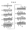
- Fig. 5 illustrates a plurality of steps of producing transfer type optical recording medium 11b in the case where the optical recording layer 4 is formed by an etching method.
- the upper surface of the base film 12 is subjected to peeling process to form a peeling layer 13 (a step of peeling treatment) (see Fig. 5(a)).
- an optical pattern support layer 22 comprising a resin having high light absorptivity or high pearmeability relative to reading light is formed on the peeling layer 13 (a step of forming an optical information support layer) (see Fig. 5(b)).
- the optical pattern support layer 22 serves to support a reflective layer 21 which has shortage in mechanical strength by itself and increases smoothness of the reflective film 21. Further, it is possible to have high absorptibity or high pearmeability relative to reading light.
- the etching process or a resist lift-off process to be described later is practiced by utilizing the portion where a reflective film is existent and the portion where any reflective film is not existent as data.
- the support layer has high absorptivity or high pearmeability relative to reading light.
- optical information pattern support layer 22 can have a function as peeling layer. In this case the step of peeling treatment as shown in Fig. 5(a) is not required.
- a reflective film 21 comprising metallic material having high reflectivity relative to reading light is formed on the optical information pattern support layer 22 by vacuum depositing or the like process (a step of coating a reflective film) (Fig. 5(c)).
- resist 23 is coated on the reflective film 21 by roll coating (a step of coating resist) (Fig. 5(d)).
- the resist 23 may be either of positive type or of negative type.
- a mask 24 having a pattern representive of optical information is placed on the resist 23 in close contact therewith and it is exposed to light beam (a step of allowing the mask to be exposed to light beam) (Fig. 5(e)).
- the thus exposed resist 23 is developed.
- This enables the optical information pattern to be transferred to the resits 23 whereby a rugged configuration corresponding to the optical informations is produced on the resist 23.
- the recessed part has no resist due to removal of the latter, causing the surface of the reflective film 21 to be exposed to the outside but the residual part of the reflective film 21 is coated still with the resist 23 (a step of developing) (see Fig. 5(f)).
- the reflective film 21 is subjected to etching from the above of the resist 23.
- Fig. 6 illustrates a plurality of steps of producing transfer type optical recording medium 11c in the case where the optical recording layer 4 is formed in accordance with the resis lift-off process.
- the upper surface of the base film 12 is subjected to peeling process to form a peeling layer 13 (a step of peeling treatment) (see Fig. 6(a)).
- an optical information pattern support layer 22 comprising a resin having high light absorptivity or high pearmeability relative to reading light is formed on the peeling layer 13 (a step of forming an optical information support layer) (see Fig. 6 (b)).
- the optical information pattern support layer 22 can serve as a peeling layer. In this case the step of peeling as shown in Fig. 6(a) is not required.
- resist is placed on the optical information pattern support layer 22 by employing a spin coating process (a step of resist coating) (see Fig. 6(c)).
- the resist 23 may be either of positive type or of negative type.
- a mask 24 having a pattern representative of optical informations is placed on the resist 23 in close contact therewith and it is then exposed to light beam (a step of allowing the mask to be exposed to light beam) (see Fig. 6(d)).
- the thus exposed resist 23 is developed.
- This enables the optical information pattern to be transferred to the resist 23 whereby a rugged configuration corresponding to the optical informations is produced on the resist 23.
- the recessed part has no resist due to removal of the latter, causing the surface of the optical information pattern support layer 22 to exposed to the outside but the residual part of the optical information pattern support layer 22 is coated still with the resist 23 (a step of developing) (see Fig. 6(e)).
- a reflective film 21 comprising metallic material having high reflectivity relative to light is formed on the resist 23 by vacuum depositing (a step of coating a reflective film) (see Fig. 6 (f)).
- the resist 23 is removed by a lift-off process.
- the part of the reflective film 21 located on the resist 23 is removed together with the resist 23 whereby the surface of the optical information pattern support layer 22 becomes exposed to the outside.
- the part of the reflective film 21 which is not located on the resist 23 resides in such a state that it is vacuum deposited on the surface of the optical information pattern support layer 22 whereby an optical reflective layer 15 is built (a step of lift-off) (see Fig. 6(g)).
- transparent adhesive is coated from the above of the residual reflective film 21 (optical reflective layer 15) to form an adhesive layer 14 (a step of coating an adhesive) (see Fig. (h)).
- a transfer type optical recording medium 11c is produced by way of the steps as mentioned above.
- the optical information pattern as mentioned above may be either preformatting pit pattern or data pit pattern.
- a protective layer 3 comprising plastics or the like having high pearmeability such as polycarbonate or the like is previously provided and a transfer type optical recording medium 11 is superimposed one above another with an adhesive layer 14 superimposed therebetween. Thereafter, heat and pressure are applied to the thus superimposed structure so as to allow the protective layer 3 and the transfer type optical recording medium 11 to be adhesively connected to one another and after completion of adhesive connection the base film 12 is peeled off together with the peeling layer 13.
- the protective layer 3 may be adhesively superimposed on the transfer type optical recording medium 11 after the peeling layer 13 is peeled off from the latter.
- the peeling layer 13 may be located on the base film 12 or it may reside on the optical information pattern support layer 22.
- a protective layer polycarbonate having a thickness of 0.5 mm was used, while as a card base white and hard polyvinylchloride having a thickness of 0.25 mm of which adhesive surface was coated with urethane-based adhesive having a thickness of 5 microns was used.
- a transfer type optical recording medium was temporarily attached to a protective layer using a hot plate made of metallic material, rubber board, rubber roll or the like each of which was heated to about 100 °C. It should be noted that at this moment only slight pressing force was required to such an extent that the transfer type optical recording medium was temporarily secured to the protective layer and therefore it was not required that the former was fixedly secured to the latter. After completion of temporal adhesive secuing the base film was peeled off.
- the protective layer and the card base were thermally adhered to one another in such a manner that they were clamped between mirror surface plates. At this moment the optical recording layer was interposed between the protective layer and the card base. Thermal adhering was achieved at pressure of 30 Kg/cm2 and temperature of 110 °C for a period of time of 10 minutes. Thereafter, heating was interrrupted and cooling was effected for a period of time of 15 minutes using water. Finally, the material was cut to dimensions corresponding to a card. Thus, a required card was obtained.
- the present invention offers the following advantageous effects.
- the method of producing an optical recording card using a transfer type optical recording medium as constructed in the above-described manner it is possible to attach the optical recording medium to a card by transfering operation.
- producing of the optical recording card can be effected at a high productive efficiency. Since the peeling layer of the base film is located opposite to the reading side of the optical recording layer, it is assured that residual foreign material relative to the peeling layer does not hinder entrance and reflection of reading light and no contamination takes place due to adherence of dust or the like to the residual foreign material of the peeling layer.
- the transfer type optical recording medium of the invention does not have any hard and thick protective layer, it is possible to form the transfer type optical recording medium in tape-shape. This means that the transfer type optical recording medium can be wound about a reel. Therefore, it is easy to handle the transfer type optical recording medium during a step of producing an optical recording card. Further, since the protective layer can be reserved or treated separately from the transfer type optical recording medium, there is no fear of injuring or degrading the protective layer with the result that an optical recording card can be obtained with a rate of occurrance of error during data reading being minimized.
- a transfer type optical recording medium can be preserved at all time regardless of how a thickness of the protective layer differs from product to product, all that is required is to adhere it to a protective layer having a predetermined thickness in response to the specification of a product. Accordingly, a countermeasure against change in thickness of the protective layer of a product can be taken quickly.
- a protective layer has the same size as a card base and a transfer type optical recording medium is prepared smaller than the protective layer, it is very easily achieved by preparing the transfer type optical recording medium separately from the protective layer in accordance with the present invention that an optical recording layer is kept in a closely sealed state within the optical recording card while the protective layer and the card base are fused together along the peripheral part of the optical recording card.
Landscapes
- Engineering & Computer Science (AREA)
- Manufacturing & Machinery (AREA)
- General Health & Medical Sciences (AREA)
- Physics & Mathematics (AREA)
- Chemical & Material Sciences (AREA)
- Health & Medical Sciences (AREA)
- Toxicology (AREA)
- Theoretical Computer Science (AREA)
- Electromagnetism (AREA)
- General Physics & Mathematics (AREA)
- Chemical Kinetics & Catalysis (AREA)
- General Chemical & Material Sciences (AREA)
- Inorganic Chemistry (AREA)
- Credit Cards Or The Like (AREA)
- Manufacturing Optical Record Carriers (AREA)
- Optical Record Carriers And Manufacture Thereof (AREA)
- Thermal Transfer Or Thermal Recording In General (AREA)
Priority Applications (1)
| Application Number | Priority Date | Filing Date | Title |
|---|---|---|---|
| AT87305372T ATE82813T1 (de) | 1986-06-17 | 1987-06-17 | Verfahren zur herstellung einer karte mit optischer aufzeichnung und optisches aufzeichnungsmedium vom transfertyp. |
Applications Claiming Priority (2)
| Application Number | Priority Date | Filing Date | Title |
|---|---|---|---|
| JP61141009A JPH0614414B2 (ja) | 1986-06-17 | 1986-06-17 | 転写型光記録媒体 |
| JP141009/86 | 1986-06-17 |
Publications (3)
| Publication Number | Publication Date |
|---|---|
| EP0250227A2 true EP0250227A2 (de) | 1987-12-23 |
| EP0250227A3 EP0250227A3 (en) | 1989-07-26 |
| EP0250227B1 EP0250227B1 (de) | 1992-11-25 |
Family
ID=15282066
Family Applications (1)
| Application Number | Title | Priority Date | Filing Date |
|---|---|---|---|
| EP87305372A Expired - Lifetime EP0250227B1 (de) | 1986-06-17 | 1987-06-17 | Verfahren zur Herstellung einer Karte mit optischer Aufzeichnung und optisches Aufzeichnungsmedium vom Transfertyp |
Country Status (6)
| Country | Link |
|---|---|
| US (1) | US5110707A (de) |
| EP (1) | EP0250227B1 (de) |
| JP (1) | JPH0614414B2 (de) |
| AT (1) | ATE82813T1 (de) |
| CA (1) | CA1300264C (de) |
| DE (1) | DE3782769T2 (de) |
Cited By (5)
| Publication number | Priority date | Publication date | Assignee | Title |
|---|---|---|---|---|
| EP0412539A3 (en) * | 1989-08-11 | 1991-12-04 | Hitachi Maxell Ltd. | Thermal recording medium |
| EP0368570A3 (de) * | 1988-11-10 | 1992-03-11 | Kyodo Printing Co., Ltd. | Optische Karte |
| WO1996014993A1 (en) * | 1994-11-16 | 1996-05-23 | Imperial Chemical Industries Plc | Cards |
| EP0864997A3 (de) * | 1997-03-14 | 1999-10-20 | Canon Kabushiki Kaisha | Informationsaufzeichungsträger und Herstellungsverfahren |
| WO2012019588A3 (de) * | 2010-08-02 | 2012-06-07 | Bundesdruckerei Gmbh | Haftvermittlerschicht für die verbindung eines holografischen datenträgers mit einem substrat |
Families Citing this family (11)
| Publication number | Priority date | Publication date | Assignee | Title |
|---|---|---|---|---|
| JP2701027B2 (ja) * | 1987-06-17 | 1998-01-21 | 共同印刷株式会社 | 光記録カードの製造方法 |
| GB9211506D0 (en) * | 1992-05-30 | 1992-07-15 | Univ Keele | Bar code |
| US5783371A (en) * | 1994-07-29 | 1998-07-21 | Trustees Of Boston University | Process for manufacturing optical data storage disk stamper |
| US5723945A (en) * | 1996-04-09 | 1998-03-03 | Electro Plasma, Inc. | Flat-panel display |
| US5962181A (en) * | 1996-04-23 | 1999-10-05 | Agfa-Gevaert, N.V. | Process for the preparation of a metal heat mode recording element |
| US6310854B1 (en) * | 1997-11-28 | 2001-10-30 | Yamaha Corporation | Optical disk having areas of different recording densities or functions |
| US7081278B2 (en) * | 2002-09-25 | 2006-07-25 | Asml Holdings N.V. | Method for protection of adhesives used to secure optics from ultra-violet light |
| JP2006099926A (ja) * | 2004-09-06 | 2006-04-13 | Sanyo Electric Co Ltd | 光磁気記録媒体および層構造 |
| FR2894515B1 (fr) * | 2005-12-08 | 2008-02-15 | Essilor Int | Procede de transfert d'un motif micronique sur un article optique et article optique ainsi obtenu |
| KR100863570B1 (ko) * | 2006-12-19 | 2008-10-15 | 삼성전자주식회사 | 와이어 그리드 편광자의 제조방법 |
| CN102446521A (zh) * | 2011-12-27 | 2012-05-09 | 浙江华虹光电集团有限公司 | 数字多功能光盘及其制造方法 |
Family Cites Families (12)
| Publication number | Priority date | Publication date | Assignee | Title |
|---|---|---|---|---|
| GB1244545A (en) * | 1968-12-25 | 1971-09-02 | Omron Tateisi Electronics Co | Information card |
| BE755709A (fr) * | 1969-10-29 | 1971-02-15 | Shipley Co | Procede d'application d'une reserve photographique sur un support et produit obtenu |
| JPS6020735B2 (ja) * | 1976-06-28 | 1985-05-23 | 富士写真フイルム株式会社 | 剥離現像可能な感光材料を用いる画像形成方法 |
| DE2758575A1 (de) * | 1977-12-29 | 1979-07-05 | Hoechst Ag | Lichtempfindliches schichtuebertragungsmaterial |
| JPS56165941A (en) * | 1980-05-22 | 1981-12-19 | Sanyo Electric Co Ltd | Production of information medium |
| US4282310A (en) * | 1980-06-30 | 1981-08-04 | American Photo-Graphics Corporation | Method of making pressure-sensitive transfer sheets |
| ATE17211T1 (de) * | 1981-07-20 | 1986-01-15 | Interlock Sicherheitssyst | Verfahren zur herstellung eines kartenfoermigen informationstraegers. |
| US4419436A (en) * | 1982-01-22 | 1983-12-06 | Kranser Leonard S | Photosensitive plate |
| US4511641A (en) * | 1983-02-02 | 1985-04-16 | Minnesota Mining And Manufacturing Company | Metal film imaging structure |
| JPS6058894A (ja) * | 1983-09-12 | 1985-04-05 | Dainippon Printing Co Ltd | 光学記録層転写用シ−ト |
| US4656114A (en) * | 1984-06-11 | 1987-04-07 | Minnesota Mining And Manufacturing Company | Presensitized color-proofing diazo resin sheet with acrylic thermal adhesive layer |
| JPH0770092B2 (ja) * | 1984-09-28 | 1995-07-31 | 共同印刷株式会社 | 光読み取りカ−ド及びその製造方法 |
-
1986
- 1986-06-17 JP JP61141009A patent/JPH0614414B2/ja not_active Expired - Lifetime
-
1987
- 1987-06-16 CA CA000539823A patent/CA1300264C/en not_active Expired - Lifetime
- 1987-06-17 AT AT87305372T patent/ATE82813T1/de not_active IP Right Cessation
- 1987-06-17 EP EP87305372A patent/EP0250227B1/de not_active Expired - Lifetime
- 1987-06-17 DE DE8787305372T patent/DE3782769T2/de not_active Expired - Fee Related
-
1990
- 1990-01-26 US US07/471,037 patent/US5110707A/en not_active Expired - Fee Related
Cited By (7)
| Publication number | Priority date | Publication date | Assignee | Title |
|---|---|---|---|---|
| EP0368570A3 (de) * | 1988-11-10 | 1992-03-11 | Kyodo Printing Co., Ltd. | Optische Karte |
| EP0412539A3 (en) * | 1989-08-11 | 1991-12-04 | Hitachi Maxell Ltd. | Thermal recording medium |
| US5246766A (en) * | 1989-08-11 | 1993-09-21 | Hitachi Maxell Ltd. | Thermal recording medium |
| WO1996014993A1 (en) * | 1994-11-16 | 1996-05-23 | Imperial Chemical Industries Plc | Cards |
| EP0864997A3 (de) * | 1997-03-14 | 1999-10-20 | Canon Kabushiki Kaisha | Informationsaufzeichungsträger und Herstellungsverfahren |
| US6146741A (en) * | 1997-03-14 | 2000-11-14 | Canon Kabushiki Kaisha | Information recording medium and production process thereof |
| WO2012019588A3 (de) * | 2010-08-02 | 2012-06-07 | Bundesdruckerei Gmbh | Haftvermittlerschicht für die verbindung eines holografischen datenträgers mit einem substrat |
Also Published As
| Publication number | Publication date |
|---|---|
| JPS62298039A (ja) | 1987-12-25 |
| DE3782769T2 (de) | 1993-04-29 |
| EP0250227A3 (en) | 1989-07-26 |
| DE3782769D1 (de) | 1993-01-07 |
| EP0250227B1 (de) | 1992-11-25 |
| US5110707A (en) | 1992-05-05 |
| CA1300264C (en) | 1992-05-05 |
| ATE82813T1 (de) | 1992-12-15 |
| JPH0614414B2 (ja) | 1994-02-23 |
Similar Documents
| Publication | Publication Date | Title |
|---|---|---|
| EP0250227B1 (de) | Verfahren zur Herstellung einer Karte mit optischer Aufzeichnung und optisches Aufzeichnungsmedium vom Transfertyp | |
| EP0485366B1 (de) | Prozess zum Herstellen von optischen Datenkarten | |
| US5474873A (en) | Optical recording material and method for producing same | |
| US5843626A (en) | Method for manufacturing a master disc for optical discs | |
| US4998239A (en) | Optical information recording medium containing a metal alloy as a reflective material | |
| US6309496B1 (en) | Method and apparatus for making dual layer DVD discs | |
| JPH08273319A (ja) | 光読取式の薄膜ディジタル・データ記録媒体及び再生アダプタ | |
| US4877713A (en) | Preformatted optical recording card and method of producing the same | |
| US5156941A (en) | Method of producing an optical or magneto-optical recording card and transfer type optical or magneto-optical recording medium | |
| EP0251794B1 (de) | Herstellungsmethode für eine optische Aufzeichnungskarte | |
| EP0650143B1 (de) | Hybrides Informationsaufzeichnungsmedium | |
| US5776575A (en) | Information recording medium and process for production thereof | |
| JP2701027B2 (ja) | 光記録カードの製造方法 | |
| JPH0997452A (ja) | 多層光学記録媒体の製造方法 | |
| EP0300733B1 (de) | Optischer Aufzeichnungsträger, Verfahren zu seiner Herstellung und sein optisches Aufzeichnungs- und Wiedergabesystem | |
| EP0404951B1 (de) | Optisches speichermedium und verfahren zu seiner herstellung | |
| JPH0770091B2 (ja) | 光読み取りカ−ド及びその製造法 | |
| JPH0452238B2 (de) | ||
| JPS63113831A (ja) | 光カ−ド | |
| US5249176A (en) | Optical recording medium, process for preparing the same and its optical recording and reproducing system | |
| JPH0615991A (ja) | 偽造防止ホログラム付光カード基体の製造方法およびその基体を用いる光情報記録媒体の製造方法 | |
| JPS62129954A (ja) | 光デイスクおよびその製造方法 | |
| JPH0693301B2 (ja) | 光カ−ドの製造方法 | |
| JPH0626021U (ja) | 光情報記録担体 | |
| JPH07114748A (ja) | 光ディスク |
Legal Events
| Date | Code | Title | Description |
|---|---|---|---|
| PUAI | Public reference made under article 153(3) epc to a published international application that has entered the european phase |
Free format text: ORIGINAL CODE: 0009012 |
|
| 17P | Request for examination filed |
Effective date: 19870707 |
|
| AK | Designated contracting states |
Kind code of ref document: A2 Designated state(s): AT BE CH DE FR GB IT LI NL SE |
|
| PUAL | Search report despatched |
Free format text: ORIGINAL CODE: 0009013 |
|
| AK | Designated contracting states |
Kind code of ref document: A3 Designated state(s): AT BE CH DE FR GB IT LI NL SE |
|
| 17Q | First examination report despatched |
Effective date: 19910325 |
|
| GRAA | (expected) grant |
Free format text: ORIGINAL CODE: 0009210 |
|
| AK | Designated contracting states |
Kind code of ref document: B1 Designated state(s): AT BE CH DE FR GB IT LI NL SE |
|
| REF | Corresponds to: |
Ref document number: 82813 Country of ref document: AT Date of ref document: 19921215 Kind code of ref document: T |
|
| REF | Corresponds to: |
Ref document number: 3782769 Country of ref document: DE Date of ref document: 19930107 |
|
| ET | Fr: translation filed | ||
| ITF | It: translation for a ep patent filed | ||
| PLBE | No opposition filed within time limit |
Free format text: ORIGINAL CODE: 0009261 |
|
| STAA | Information on the status of an ep patent application or granted ep patent |
Free format text: STATUS: NO OPPOSITION FILED WITHIN TIME LIMIT |
|
| 26N | No opposition filed | ||
| EAL | Se: european patent in force in sweden |
Ref document number: 87305372.2 |
|
| PGFP | Annual fee paid to national office [announced via postgrant information from national office to epo] |
Ref country code: GB Payment date: 19970609 Year of fee payment: 11 |
|
| PGFP | Annual fee paid to national office [announced via postgrant information from national office to epo] |
Ref country code: FR Payment date: 19970610 Year of fee payment: 11 |
|
| PGFP | Annual fee paid to national office [announced via postgrant information from national office to epo] |
Ref country code: AT Payment date: 19970611 Year of fee payment: 11 |
|
| PGFP | Annual fee paid to national office [announced via postgrant information from national office to epo] |
Ref country code: SE Payment date: 19970618 Year of fee payment: 11 |
|
| PGFP | Annual fee paid to national office [announced via postgrant information from national office to epo] |
Ref country code: NL Payment date: 19970630 Year of fee payment: 11 Ref country code: CH Payment date: 19970630 Year of fee payment: 11 |
|
| PGFP | Annual fee paid to national office [announced via postgrant information from national office to epo] |
Ref country code: BE Payment date: 19970812 Year of fee payment: 11 |
|
| PG25 | Lapsed in a contracting state [announced via postgrant information from national office to epo] |
Ref country code: GB Free format text: LAPSE BECAUSE OF NON-PAYMENT OF DUE FEES Effective date: 19980617 Ref country code: AT Free format text: LAPSE BECAUSE OF NON-PAYMENT OF DUE FEES Effective date: 19980617 |
|
| PG25 | Lapsed in a contracting state [announced via postgrant information from national office to epo] |
Ref country code: SE Free format text: LAPSE BECAUSE OF NON-PAYMENT OF DUE FEES Effective date: 19980618 |
|
| PG25 | Lapsed in a contracting state [announced via postgrant information from national office to epo] |
Ref country code: LI Free format text: LAPSE BECAUSE OF NON-PAYMENT OF DUE FEES Effective date: 19980630 Ref country code: CH Free format text: LAPSE BECAUSE OF NON-PAYMENT OF DUE FEES Effective date: 19980630 Ref country code: BE Free format text: LAPSE BECAUSE OF NON-PAYMENT OF DUE FEES Effective date: 19980630 |
|
| BERE | Be: lapsed |
Owner name: KYODO PRINTING CO. LTD Effective date: 19980630 |
|
| PG25 | Lapsed in a contracting state [announced via postgrant information from national office to epo] |
Ref country code: NL Free format text: LAPSE BECAUSE OF NON-PAYMENT OF DUE FEES Effective date: 19990101 |
|
| GBPC | Gb: european patent ceased through non-payment of renewal fee |
Effective date: 19980617 |
|
| REG | Reference to a national code |
Ref country code: CH Ref legal event code: PL |
|
| PG25 | Lapsed in a contracting state [announced via postgrant information from national office to epo] |
Ref country code: FR Free format text: LAPSE BECAUSE OF NON-PAYMENT OF DUE FEES Effective date: 19990226 |
|
| EUG | Se: european patent has lapsed |
Ref document number: 87305372.2 |
|
| NLV4 | Nl: lapsed or anulled due to non-payment of the annual fee |
Effective date: 19990101 |
|
| REG | Reference to a national code |
Ref country code: FR Ref legal event code: ST |
|
| PGFP | Annual fee paid to national office [announced via postgrant information from national office to epo] |
Ref country code: DE Payment date: 19990618 Year of fee payment: 13 |
|
| PG25 | Lapsed in a contracting state [announced via postgrant information from national office to epo] |
Ref country code: DE Free format text: LAPSE BECAUSE OF NON-PAYMENT OF DUE FEES Effective date: 20010403 |
|
| PG25 | Lapsed in a contracting state [announced via postgrant information from national office to epo] |
Ref country code: IT Free format text: LAPSE BECAUSE OF NON-PAYMENT OF DUE FEES Effective date: 20050617 |