EP0252679B1 - Dispositif semi-conducteur ayant deux électrodes séparées par un film isolant - Google Patents
Dispositif semi-conducteur ayant deux électrodes séparées par un film isolant Download PDFInfo
- Publication number
- EP0252679B1 EP0252679B1 EP87305826A EP87305826A EP0252679B1 EP 0252679 B1 EP0252679 B1 EP 0252679B1 EP 87305826 A EP87305826 A EP 87305826A EP 87305826 A EP87305826 A EP 87305826A EP 0252679 B1 EP0252679 B1 EP 0252679B1
- Authority
- EP
- European Patent Office
- Prior art keywords
- film
- floating gate
- volatile memory
- polycide
- memory device
- Prior art date
- Legal status (The legal status is an assumption and is not a legal conclusion. Google has not performed a legal analysis and makes no representation as to the accuracy of the status listed.)
- Expired - Lifetime
Links
Images
Classifications
-
- H—ELECTRICITY
- H10—SEMICONDUCTOR DEVICES; ELECTRIC SOLID-STATE DEVICES NOT OTHERWISE PROVIDED FOR
- H10P—GENERIC PROCESSES OR APPARATUS FOR THE MANUFACTURE OR TREATMENT OF DEVICES COVERED BY CLASS H10
- H10P14/00—Formation of materials, e.g. in the shape of layers or pillars
- H10P14/60—Formation of materials, e.g. in the shape of layers or pillars of insulating materials
- H10P14/69—Inorganic materials
- H10P14/692—Inorganic materials composed of oxides, glassy oxides or oxide-based glasses
- H10P14/6921—Inorganic materials composed of oxides, glassy oxides or oxide-based glasses containing silicon
- H10P14/69215—Inorganic materials composed of oxides, glassy oxides or oxide-based glasses containing silicon the material being a silicon oxide, e.g. SiO2
-
- H—ELECTRICITY
- H10—SEMICONDUCTOR DEVICES; ELECTRIC SOLID-STATE DEVICES NOT OTHERWISE PROVIDED FOR
- H10D—INORGANIC ELECTRIC SEMICONDUCTOR DEVICES
- H10D1/00—Resistors, capacitors or inductors
- H10D1/60—Capacitors
- H10D1/68—Capacitors having no potential barriers
-
- H—ELECTRICITY
- H10—SEMICONDUCTOR DEVICES; ELECTRIC SOLID-STATE DEVICES NOT OTHERWISE PROVIDED FOR
- H10D—INORGANIC ELECTRIC SEMICONDUCTOR DEVICES
- H10D64/00—Electrodes of devices having potential barriers
- H10D64/60—Electrodes characterised by their materials
- H10D64/66—Electrodes having a conductor capacitively coupled to a semiconductor by an insulator, e.g. MIS electrodes
- H10D64/661—Electrodes having a conductor capacitively coupled to a semiconductor by an insulator, e.g. MIS electrodes the conductor comprising a layer of silicon contacting the insulator, e.g. polysilicon having vertical doping variation
- H10D64/662—Electrodes having a conductor capacitively coupled to a semiconductor by an insulator, e.g. MIS electrodes the conductor comprising a layer of silicon contacting the insulator, e.g. polysilicon having vertical doping variation the conductor further comprising additional layers, e.g. multiple silicon layers having different crystal structures
- H10D64/663—Electrodes having a conductor capacitively coupled to a semiconductor by an insulator, e.g. MIS electrodes the conductor comprising a layer of silicon contacting the insulator, e.g. polysilicon having vertical doping variation the conductor further comprising additional layers, e.g. multiple silicon layers having different crystal structures the additional layers comprising a silicide layer contacting the layer of silicon, e.g. polycide gates
-
- H—ELECTRICITY
- H10—SEMICONDUCTOR DEVICES; ELECTRIC SOLID-STATE DEVICES NOT OTHERWISE PROVIDED FOR
- H10P—GENERIC PROCESSES OR APPARATUS FOR THE MANUFACTURE OR TREATMENT OF DEVICES COVERED BY CLASS H10
- H10P14/00—Formation of materials, e.g. in the shape of layers or pillars
- H10P14/60—Formation of materials, e.g. in the shape of layers or pillars of insulating materials
- H10P14/63—Formation of materials, e.g. in the shape of layers or pillars of insulating materials characterised by the formation processes
- H10P14/6326—Deposition processes
- H10P14/6328—Deposition from the gas or vapour phase
- H10P14/6334—Deposition from the gas or vapour phase using decomposition or reaction of gaseous or vapour phase compounds, i.e. chemical vapour deposition
-
- H—ELECTRICITY
- H10—SEMICONDUCTOR DEVICES; ELECTRIC SOLID-STATE DEVICES NOT OTHERWISE PROVIDED FOR
- H10P—GENERIC PROCESSES OR APPARATUS FOR THE MANUFACTURE OR TREATMENT OF DEVICES COVERED BY CLASS H10
- H10P14/00—Formation of materials, e.g. in the shape of layers or pillars
- H10P14/60—Formation of materials, e.g. in the shape of layers or pillars of insulating materials
- H10P14/66—Formation of materials, e.g. in the shape of layers or pillars of insulating materials characterised by the type of materials
- H10P14/668—Formation of materials, e.g. in the shape of layers or pillars of insulating materials characterised by the type of materials the materials being characterised by the deposition precursor materials
- H10P14/6681—Formation of materials, e.g. in the shape of layers or pillars of insulating materials characterised by the type of materials the materials being characterised by the deposition precursor materials the precursor containing a compound comprising Si
- H10P14/6682—Formation of materials, e.g. in the shape of layers or pillars of insulating materials characterised by the type of materials the materials being characterised by the deposition precursor materials the precursor containing a compound comprising Si the compound being a silane, e.g. disilane, methylsilane or chlorosilane
-
- H—ELECTRICITY
- H10—SEMICONDUCTOR DEVICES; ELECTRIC SOLID-STATE DEVICES NOT OTHERWISE PROVIDED FOR
- H10D—INORGANIC ELECTRIC SEMICONDUCTOR DEVICES
- H10D64/00—Electrodes of devices having potential barriers
- H10D64/60—Electrodes characterised by their materials
- H10D64/66—Electrodes having a conductor capacitively coupled to a semiconductor by an insulator, e.g. MIS electrodes
- H10D64/68—Electrodes having a conductor capacitively coupled to a semiconductor by an insulator, e.g. MIS electrodes characterised by the insulator, e.g. by the gate insulator
- H10D64/691—Electrodes having a conductor capacitively coupled to a semiconductor by an insulator, e.g. MIS electrodes characterised by the insulator, e.g. by the gate insulator comprising metallic compounds, e.g. metal oxides or metal silicates
-
- H—ELECTRICITY
- H10—SEMICONDUCTOR DEVICES; ELECTRIC SOLID-STATE DEVICES NOT OTHERWISE PROVIDED FOR
- H10D—INORGANIC ELECTRIC SEMICONDUCTOR DEVICES
- H10D64/00—Electrodes of devices having potential barriers
- H10D64/60—Electrodes characterised by their materials
- H10D64/66—Electrodes having a conductor capacitively coupled to a semiconductor by an insulator, e.g. MIS electrodes
- H10D64/68—Electrodes having a conductor capacitively coupled to a semiconductor by an insulator, e.g. MIS electrodes characterised by the insulator, e.g. by the gate insulator
- H10D64/693—Electrodes having a conductor capacitively coupled to a semiconductor by an insulator, e.g. MIS electrodes characterised by the insulator, e.g. by the gate insulator the insulator comprising nitrogen, e.g. nitrides, oxynitrides or nitrogen-doped materials
Definitions
- This invention concerns a semiconductor device such, for example, as a non-volatile memory or a capacitive component.
- a semiconductor device comprising first and second electrodes with an insulation film therebetween, at least the first electrode being formed of material comprising polycrystalline silicon.
- an insulation film made by the chemical vapour deposition (CVD) process, a polyimide film and a thermally oxidized film of polycrystalline silicon have been used as the said insulation film, while the second electrode has incorporated wiring and has been made, for example, of a conductive material such as aluminium or polycrystalline silicon.
- a thermally oxidized film of polycrystalline silicon has to be used as the insulation film because it has a good insulating performance and thickness controllability.
- polycrystalline silicon as a material for an electrode and wiring has, in certain fields, been gradually replaced by so-called polycide material, ie. material formed from polycrystalline silicon and a metal silicide.
- the polycide material may comprise a two layered structure of polycrystalline silicon and a metal silicide.
- a thermally oxidized film of polycide does not have uniform film thickness and does not have a good insulating performance. Accordingly, since the insulating performance of a thin insulating film of less than 1,000 ⁇ thickness formed by thermally oxidizing the periphery of polycide material used as the wiring and the electrode is also poor, it has been impossible to use the polycide as the material for the electrode and the wiring of a semiconductor device.
- a non-volatile device comprising floating gate and control gate electrodes with an insulation film therebetween which has been formed by a chemical vapour deposition process characterised in that the insulation film is a silicon oxide film formed by a chemical gas phase reaction using a dichlorosilane (SiH2Cl2) gas and a nitrous oxide (N2O) gas and having a thickness which does not exceed 1,000 ⁇ , the material of the floating gate electrode comprising a polycide.
- SiH2Cl2 dichlorosilane
- N2O nitrous oxide
- the first electrode has a plurality of layers.
- the first electrode may comprise a metal silicide membrane laminated to a polycrystalline silicon membrane.
- the chemical gas phase reaction may have been carried out by arranging that the relative N2O/SiH2Cl2 flow rate is at least 5.
- the said reaction has been preferably effected under a reduced pressure in the range of 0.1 mbar and 2 mbar and a temperature in the range of 700°C to 950°C.
- the said first and second electrodes incorporate wiring.
- the first electrode may be mounted directly or indirectly on a substrate.
- the semiconductor device may be a non-volatile memory having a floating gate.
- the semiconductor device of the present invention employs, as an insulation film on a polycide electrode and wiring, a silicon oxide (SiO2) film formed by using a chemical vapour deposition process (CVD) process, the silicon oxide film being formed by reacting a dichlorosilane (SiH2Cl2) gas and a nitrous oxide (N2O) gas in a chemical gas phase reaction under a high temperature atmosphere (hereinafter referred to as high temperature CVD silicon oxide film).
- the process may be carried out at a reduced pressure of from 0.1 mbar to 2 mbar and at a temperature of 700°C to 950°C.
- Such a high temperature CVD SiO2 film is advantageous because it can be given uniform film thickness and because it has an extremely satisfactory insulating performance. Accordingly, it can be used also as a thin insulating film with a thickness of less than 1000 ⁇ and it can also be formed over a polycide electrode and wiring of the semiconductor device.
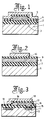
- FIG 1 there is shown a semiconductor device according to the present invention in which, after an insulation layer 2 has been formed on a substrate 1, a polycide electrode and wiring 3 is formed on the insulation layer 2.
- the polycide electrode and wiring 3, as indicated above, comprises polycrystalline silicon and a metal silicide.
- a CVD silicon oxide insulation film 4 is layered over the polycide electrode and wiring 3 by using a CVD process.
- An electrode and wiring 5 is then formed over the CVD silicon oxide insulation film 4 to obtain the semiconductor device shown in Figure 1.
- the substrate 1 shown in Figure 1 may be a semiconductor such as of silicon, germanium, gallium arsenide and indium phosphide; an insulator such as glass or aluminium; or a metal such as stainless steel or iron.
- the insulation layer 2 may be constituted by a silicon oxide film, a silicon nitride film, alumina, etc, although of course, the insulation layer 2 may be dispensed with.
- the polycide electrode and wiring 3 may be formed generally as described below.
- a polycrystalline silicon film is formed by means of a chemical vapor deposition process (CVD process) or by means of a physical vapor deposition process (PVD process), etc.
- the polycrystalline silicon film may be doped with phosphorus,arsenic or boron.
- the doping may be conducted after the formation of the polycrystalline silicon film. Generally, doping is conducted by using a diffusion process. Of course, doping of the polycrystalline silicon film may be dispensed with.
- Heat treatment of the polycrystalline silicon film may be carried out after the formation of the polycrystalline silicon film, but heat treatment may, of course be dispensed with.
- a silicide film is laminated over the polycrystalline silicon film by way of a CVD process or a PVD process.
- the silicide film usable herein can include molybdenum silicide, tungsten silicide, platinum silicide, titanium silicide, tantalum silicide, zirconium silicide and palladium silicide. Then, heat treatment may be applied to stabilize the composition which has been formed so far.
- the said polycide electrode and wiring 3 may be constituted by a dual layered film prepared by laminating a silicide membrane on a polycrystalline silicon membrane.
- Another method of preparing the polycide electrode and hiring 3 is to prepare a metal film over a polycrystalline silicon film, followed by heat treatment.
- the metal film is formed by a CVD or a PVD process.
- the metal film usable herein can include, for example, molybdenum, tungsten, platinum, titanium, tantalum, zirconium and palladium.
- the silicon oxide film 4 may be laminated to the polycide electrode and wiring 3 by using a CVD process since this shows a satisfactory insulating performance even on the polycide film.
- a silicon oxide film 4 prepared by a chemical deposition process by using a dichlorosilane (SiH2Cl2) gas and a nitrous oxide (N2O) gas has an extremely good insulating performance.
- the density of a membrane of the silicon oxide film grown from a dichlorosilane (SiH2Cl2) gas and a nitrous oxide (N2O) gas suffers from an effect arising from the pressure and temperature used upon formation.
- the silicon oxide film 4 is preferably formed under a pressure substantially within the range 0.1 mbar to 2.0 mbar and at a temperature within the range 700°C to 950°C.
- the silicon oxide film 4 prepared under the above-mentioned conditions is satisfactory so far as film thickness controllability is concerned and has adequate insulating performance and a satisfactory density. Further, if the proportion of the dichlorosilane (SiH2Cl2) gas becomes too high, the silicon oxide film 4 may contain too much silicon with the result that its insulating performance is reduced and, accordingly, a desirable insulating performance can be obtained by setting the ratio of the flow rate between N2O/SiH2Cl2 at a value of at least 5.
- a silicon oxide film 4 formed under a pressure from 0.1 mbar to 2.0 mbar and at a temperature from 700°C to 950°C has a good film thickness controllability, a thin film of less than 1000 ⁇ can be laminated uniformly over the polycide electrode and wiring 3.
- a capacitive component for use with a semiconductor device has often been used in dynamic RAMs or analog and digital circuits.
- a capacitive component using a silicon oxide film as an insulation film between electrodes, it is necessary to form a thin insulation film in order to obtain a large capacity with a small surface area and it is also required that there is little leakage of the accumulated electric charges.
- the insulation film may be formed by a CVD process using a SiH2Cl2 gas and an N2O gas in order to obtain desired capacitance characteristics.
- the reference numerals 6, 7, 8, 9 and 10 in Figure 2 respectively correspond to the reference numerals 1, 2, 3, 4, 5 in Figure 1.
- An extremely thin CVD silicon oxide film 9 having a thickness of not more than 1000 ⁇ is laminated over a polycide film 8 i.e. a film comprising polycrystalline silicon and at least one metal silicide, and, an electrode and wiring 10 is formed over the silicon oxide film 9.
- a capacitive component is formed which is constituted by the polycide film 8, the silicon oxide film 9 formed through the reaction between SiH2Cl2 gas and N2O gas, and the electrode and wiring 10. It is possible to form the silicon oxide film 9 into an extremely thin film of not more than 100 ⁇ thickness if required.
- a lateral type vacuum CVD device When a lateral type vacuum CVD device is used in conditions of growth (with a flow of SiH2Cl2 gas at 25 sccm and a flow of N2O gas at 250 sccm, under a pressure of 0.4 mbar and a temperature of 850°C), since the growth rate is 6.2 and the uniformity is not more an ⁇ 5%, a silicon oxide film of less than 100 ⁇ thickness can be formed with good controllability. Since the insulating performance of the silicon oxide film is extremely satisfactory, a capacitive component with less electric discharge can be formed within a small surface area.
- the present invention is applicable also to a non-volatile memory having a floating gate as will be clear from the description of Figure 3.
- a floating gate electrode 16 is formed from a polycide, i.e. a material comprising polycrystalline silicon and at least one metal silicide.
- the floating gate electrode 16 is formed on a silicon oxide insulation film 14 which is provided on a silicon substrate 11.
- a thin CVD silicon oxide film 17 of 100 - 500 ⁇ thickness is laminated over the floating gate electrode 16 and, further, a control gate electrode 18 is formed on the silicon oxide film 17. Electrons are injected from a dense N type impurity region 12 in the silicon substrate 11 by way of a thin silicon oxide film 15 to the floating gate electrode 16, by which the voltage of the floating gate can be changed, a drain region 13 also being provided in the silicon substrate 11.
- the device constitutes a memory whose characteristics are comparable with those of conventional memories using polysilicon as the floating gate, both in respect of repeated rewriting and of charge retention time. Further, since wiring can be made with low resistance by using the polycide, reading and rewriting can be conducted at a higher speed than usual.
- the polycide electrode and wiring can be formed by laminating two or more layers. That is, after forming the polycide at the first layer, a thin CVD silicon oxide film is laminated thereto. Then, after forming the polycide at the second layer, a thin CVD silicon oxide film is again laminated thereto. By repeating the above-described procedures, it is possible to laminate the polycide electrode and wiring to any desired number of layers.
- a three-layered polysilicon electrode and wiring has been used for non-volatile memories in recent years and it is possible to obtain a non-volatile memory of a three-layered polycide electrode and wiring by using the present invention.
- a thin silicon oxide film formed by using a CVD process can be formed as an insulation film over a polycide electrode and wiring
- the polycide electrode and wiring can be used in a device employing a thin insulation film, and a higher operational speed of the device than usual can be attained.
Landscapes
- Internal Circuitry In Semiconductor Integrated Circuit Devices (AREA)
- Electrodes Of Semiconductors (AREA)
- Semiconductor Integrated Circuits (AREA)
- Non-Volatile Memory (AREA)
- Semiconductor Memories (AREA)
Claims (8)
- Un dispositif de mémoire non volatile comprenant des électrodes de grille flottante et de grille de commande (3, 5) séparées par une couche d'isolation (4) qui a été formée par un procédé de dépôt chimique en phase vapeur, caractérisé en ce que la couche d'isolation (4) est une couche d'oxyde de silicium formée par une réaction chimique en phase gazeuse utilisant un gaz qui consiste en dichlorosilane (SiH₂Cl₂) et un gaz qui consiste en oxyde nitreux (N₂O) et ayant une épaisseur qui ne dépasse pas 100 nm, le matériau de l'électrode de grille flottante (3) consistant en une combinaison de silicium polycristallin et d'un siliciure de métal.
- Un dispositif de mémoire non volatile selon la revendication 1, caractérisé en ce que l'électrode de grille flottante (3) comprend plusieurs couches.
- Un dispositif de mémoire non volatile selon la revendication 2, caractérisé en ce que l'électrode de grille flottante (3) comprend une pellicule de siliciure de métal déposée sur une pellicule de silicium polycristallin.
- Un dispositif de mémoire non volatile selon l'une quelconque des revendications précédentes, caractérisé en ce que la réaction chimique en phase gazeuse a été accomplie en fixant le rapport de débit N₂O/SiH₂Cl₂ à une valeur au moins égale à 5.
- Un dispositif de mémoire non volatile selon l'une quelconque des revendications précédentes, caractérisé en ce que la réaction précitée a été effectuée sous une pression réduite dans la plage de 0,1 hPa à 2 hPa, et à une température dans la plage de 700°C à 950°C.
- Un dispositif de mémoire non volatile selon l'une quelconque des revendications précédentes, caractérisé en ce que les électrodes de grille flottante et de grille de commande ( 3, 5 ) comprennent des interconnexions.
- Un dispositif de mémoire non volatile selon l'une quelconque des revendications précédentes, caractérisé en ce que l'électrode de grille flottante (3) est montée directement ou indirectement sur un substrat (1).
- Un procédé de fabrication d'un dispositif de mémoire non volatile qui comprend des électrodes de grille flottante et de grille de commande (3, 5) séparées par une couche d'isolation (4) qui a été formée par un procédé de dépôt chimique en phase vapeur, caractérisé en ce que la couche d'isolation (4) est une couche d'oxyde de silicium formée par une réaction chimique en phase gazeuse utilisant un gaz qui consiste en dichlorosilane (SiH₂Cl₂) et un gaz qui consiste en oxyde nitreux (N₂O), et ayant une épaisseur qui ne dépasse pas 100 nm, le matériau de l'électrode de grille flottante (3) consistant en une combinaison de silicium polycristallin et de siliciure de métal.
Applications Claiming Priority (2)
| Application Number | Priority Date | Filing Date | Title |
|---|---|---|---|
| JP162472/86 | 1986-07-10 | ||
| JP61162472A JP2518617B2 (ja) | 1986-07-10 | 1986-07-10 | 不揮発性メモリおよびその製造方法 |
Publications (3)
| Publication Number | Publication Date |
|---|---|
| EP0252679A2 EP0252679A2 (fr) | 1988-01-13 |
| EP0252679A3 EP0252679A3 (en) | 1988-08-17 |
| EP0252679B1 true EP0252679B1 (fr) | 1993-05-05 |
Family
ID=15755275
Family Applications (1)
| Application Number | Title | Priority Date | Filing Date |
|---|---|---|---|
| EP87305826A Expired - Lifetime EP0252679B1 (fr) | 1986-07-10 | 1987-07-01 | Dispositif semi-conducteur ayant deux électrodes séparées par un film isolant |
Country Status (4)
| Country | Link |
|---|---|
| US (1) | US5001527A (fr) |
| EP (1) | EP0252679B1 (fr) |
| JP (1) | JP2518617B2 (fr) |
| DE (1) | DE3785699T2 (fr) |
Families Citing this family (13)
| Publication number | Priority date | Publication date | Assignee | Title |
|---|---|---|---|---|
| JP2779623B2 (ja) * | 1988-06-06 | 1998-07-23 | セイコーインスツルメンツ株式会社 | 半導体不揮発性メモリ |
| JPH02156564A (ja) * | 1988-12-08 | 1990-06-15 | Matsushita Electric Ind Co Ltd | 半導体記憶装置の製造方法 |
| JPH0322435A (ja) * | 1989-06-19 | 1991-01-30 | Nec Corp | 半導体装置 |
| US5057447A (en) * | 1990-07-09 | 1991-10-15 | Texas Instruments Incorporated | Silicide/metal floating gate process |
| US5086370A (en) * | 1990-08-24 | 1992-02-04 | Analog Devices, Incorporated | Integrated circuit chip formed with a capacitor having a low voltage coefficient, and method of making such capacitor |
| US5218511A (en) * | 1992-06-22 | 1993-06-08 | Vlsi Technology, Inc. | Inter-silicide capacitor |
| US5470775A (en) * | 1993-11-09 | 1995-11-28 | Vlsi Technology, Inc. | Method of forming a polysilicon-on-silicide capacitor |
| US5498558A (en) * | 1994-05-06 | 1996-03-12 | Lsi Logic Corporation | Integrated circuit structure having floating electrode with discontinuous phase of metal silicide formed on a surface thereof and process for making same |
| DE19536465A1 (de) * | 1995-09-29 | 1997-04-03 | Siemens Ag | Integrierbarer Kondensator und Verfahren zu seiner Herstellung |
| DE19536528A1 (de) * | 1995-09-29 | 1997-04-03 | Siemens Ag | Integrierbarer Kondensator und Verfahren zu seiner Herstellung |
| JP3241316B2 (ja) | 1998-01-07 | 2001-12-25 | 日本電気株式会社 | フラッシュメモリの製造方法 |
| US6884295B2 (en) | 2000-05-29 | 2005-04-26 | Tokyo Electron Limited | Method of forming oxynitride film or the like and system for carrying out the same |
| US7071117B2 (en) * | 2004-02-27 | 2006-07-04 | Micron Technology, Inc. | Semiconductor devices and methods for depositing a dielectric film |
Family Cites Families (14)
| Publication number | Priority date | Publication date | Assignee | Title |
|---|---|---|---|---|
| US4288256A (en) * | 1977-12-23 | 1981-09-08 | International Business Machines Corporation | Method of making FET containing stacked gates |
| US4282540A (en) * | 1977-12-23 | 1981-08-04 | International Business Machines Corporation | FET Containing stacked gates |
| JPS56150851A (en) * | 1980-04-22 | 1981-11-21 | Toshiba Corp | Manufacture of semiconductor integrated circuit |
| US4419385A (en) * | 1981-09-24 | 1983-12-06 | Hughes Aircraft Company | Low temperature process for depositing an oxide dielectric layer on a conductive surface and multilayer structures formed thereby |
| JPS5935469A (ja) * | 1982-08-24 | 1984-02-27 | Toshiba Corp | 半導体装置 |
| JPS5978576A (ja) * | 1982-10-27 | 1984-05-07 | Toshiba Corp | 半導体装置およびその製造方法 |
| US4577390A (en) * | 1983-02-23 | 1986-03-25 | Texas Instruments Incorporated | Fabrication of polysilicon to polysilicon capacitors with a composite dielectric layer |
| JPS59161860A (ja) * | 1983-03-07 | 1984-09-12 | Hitachi Ltd | 半導体メモリ装置 |
| JPS6058644A (ja) * | 1983-09-12 | 1985-04-04 | Toshiba Corp | 半導体装置 |
| JPS6066435A (ja) * | 1983-09-22 | 1985-04-16 | Matsushita Electric Ind Co Ltd | 薄膜形成方法 |
| JPS60105279A (ja) * | 1983-11-14 | 1985-06-10 | Toshiba Corp | 半導体装置 |
| JPS60158672A (ja) * | 1984-01-27 | 1985-08-20 | Seiko Instr & Electronics Ltd | 半導体装置の製造方法 |
| JPS61131487A (ja) * | 1984-11-29 | 1986-06-19 | Res Dev Corp Of Japan | 半導体不揮発性メモリ |
| JP2570263B2 (ja) * | 1986-05-07 | 1997-01-08 | 富士通株式会社 | 半導体装置およびその製造方法 |
-
1986
- 1986-07-10 JP JP61162472A patent/JP2518617B2/ja not_active Expired - Lifetime
-
1987
- 1987-07-01 DE DE8787305826T patent/DE3785699T2/de not_active Expired - Fee Related
- 1987-07-01 EP EP87305826A patent/EP0252679B1/fr not_active Expired - Lifetime
-
1990
- 1990-08-13 US US07/569,375 patent/US5001527A/en not_active Expired - Lifetime
Also Published As
| Publication number | Publication date |
|---|---|
| DE3785699D1 (de) | 1993-06-09 |
| JPS6317544A (ja) | 1988-01-25 |
| EP0252679A3 (en) | 1988-08-17 |
| JP2518617B2 (ja) | 1996-07-24 |
| US5001527A (en) | 1991-03-19 |
| EP0252679A2 (fr) | 1988-01-13 |
| DE3785699T2 (de) | 1993-08-19 |
Similar Documents
| Publication | Publication Date | Title |
|---|---|---|
| US5736449A (en) | Semiconductor memory device having improved isolation between electrodes, and process for fabricating the same | |
| KR100200060B1 (ko) | 높은 캐패시턴스 값을 지니는 탄탈 산화물 캐패시터 | |
| US5187638A (en) | Barrier layers for ferroelectric and pzt dielectric on silicon | |
| US6451646B1 (en) | High-k dielectric materials and processes for manufacturing them | |
| US5486488A (en) | Process for manufacturing semiconductor device | |
| US6140671A (en) | Semiconductor memory device having capacitive storage therefor | |
| KR920005320B1 (ko) | 캐패시터 및 그 제조방법 | |
| EP0252679B1 (fr) | Dispositif semi-conducteur ayant deux électrodes séparées par un film isolant | |
| US6773981B1 (en) | Methods of forming capacitors | |
| US6670668B2 (en) | Microelectronic structure, method for fabricating it and its use in a memory cell | |
| JPH0685173A (ja) | 半導体集積回路用キャパシタ | |
| US5343353A (en) | Semiconductor device and process of producing the same | |
| JP2861129B2 (ja) | 半導体装置 | |
| JPH04326766A (ja) | 半導体装置及びその製造方法 | |
| US6943392B2 (en) | Capacitors having a capacitor dielectric layer comprising a metal oxide having multiple different metals bonded with oxygen | |
| US6194736B1 (en) | Quantum conductive recrystallization barrier layers | |
| US6011289A (en) | Metal oxide stack for flash memory application | |
| JPH0563157A (ja) | 半導体装置 | |
| US6316802B1 (en) | Easy to manufacture integrated semiconductor memory configuration with platinum electrodes | |
| US20040150108A1 (en) | Low resistance barrier for a microelectronic component and method for fabricating the same | |
| US20020135031A1 (en) | Method for forming a dielectric layer and semiconductor device incorporating the same | |
| KR960004461B1 (ko) | 폴리실리콘상에 평탄한 경계면을 갖고 있는 집적 회로 및 이의 제조 방법 | |
| JP3415476B2 (ja) | 半導体装置の製造方法 | |
| JPH0736438B2 (ja) | 半導体装置 | |
| KR940011799B1 (ko) | TiN층으로 된 전하저장전극 형성방법 |
Legal Events
| Date | Code | Title | Description |
|---|---|---|---|
| PUAI | Public reference made under article 153(3) epc to a published international application that has entered the european phase |
Free format text: ORIGINAL CODE: 0009012 |
|
| AK | Designated contracting states |
Kind code of ref document: A2 Designated state(s): DE GB |
|
| PUAL | Search report despatched |
Free format text: ORIGINAL CODE: 0009013 |
|
| AK | Designated contracting states |
Kind code of ref document: A3 Designated state(s): DE GB |
|
| 17P | Request for examination filed |
Effective date: 19890118 |
|
| 17Q | First examination report despatched |
Effective date: 19910912 |
|
| GRAA | (expected) grant |
Free format text: ORIGINAL CODE: 0009210 |
|
| AK | Designated contracting states |
Kind code of ref document: B1 Designated state(s): DE GB |
|
| REF | Corresponds to: |
Ref document number: 3785699 Country of ref document: DE Date of ref document: 19930609 |
|
| PLBE | No opposition filed within time limit |
Free format text: ORIGINAL CODE: 0009261 |
|
| STAA | Information on the status of an ep patent application or granted ep patent |
Free format text: STATUS: NO OPPOSITION FILED WITHIN TIME LIMIT |
|
| 26N | No opposition filed | ||
| PGFP | Annual fee paid to national office [announced via postgrant information from national office to epo] |
Ref country code: GB Payment date: 19940621 Year of fee payment: 8 |
|
| PGFP | Annual fee paid to national office [announced via postgrant information from national office to epo] |
Ref country code: DE Payment date: 19940622 Year of fee payment: 8 |
|
| PG25 | Lapsed in a contracting state [announced via postgrant information from national office to epo] |
Ref country code: GB Effective date: 19950701 |
|
| GBPC | Gb: european patent ceased through non-payment of renewal fee |
Effective date: 19950701 |
|
| PG25 | Lapsed in a contracting state [announced via postgrant information from national office to epo] |
Ref country code: DE Effective date: 19960402 |