EP0256360A2 - Steuerbare Tunneldiode - Google Patents
Steuerbare Tunneldiode Download PDFInfo
- Publication number
- EP0256360A2 EP0256360A2 EP87110764A EP87110764A EP0256360A2 EP 0256360 A2 EP0256360 A2 EP 0256360A2 EP 87110764 A EP87110764 A EP 87110764A EP 87110764 A EP87110764 A EP 87110764A EP 0256360 A2 EP0256360 A2 EP 0256360A2
- Authority
- EP
- European Patent Office
- Prior art keywords
- semiconductor layer
- layer
- semiconductor
- semiconductor device
- region
- Prior art date
- Legal status (The legal status is an assumption and is not a legal conclusion. Google has not performed a legal analysis and makes no representation as to the accuracy of the status listed.)
- Granted
Links
Images



Classifications
-
- H—ELECTRICITY
- H10—SEMICONDUCTOR DEVICES; ELECTRIC SOLID-STATE DEVICES NOT OTHERWISE PROVIDED FOR
- H10D—INORGANIC ELECTRIC SEMICONDUCTOR DEVICES
- H10D30/00—Field-effect transistors [FET]
- H10D30/40—FETs having zero-dimensional [0D], one-dimensional [1D] or two-dimensional [2D] charge carrier gas channels
- H10D30/47—FETs having zero-dimensional [0D], one-dimensional [1D] or two-dimensional [2D] charge carrier gas channels having two-dimensional [2D] charge carrier gas channels, e.g. nanoribbon FETs or high electron mobility transistors [HEMT]
- H10D30/471—High electron mobility transistors [HEMT] or high hole mobility transistors [HHMT]
- H10D30/473—High electron mobility transistors [HEMT] or high hole mobility transistors [HHMT] having confinement of carriers by multiple heterojunctions, e.g. quantum well HEMT
- H10D30/4732—High electron mobility transistors [HEMT] or high hole mobility transistors [HHMT] having confinement of carriers by multiple heterojunctions, e.g. quantum well HEMT using Group III-V semiconductor material
-
- H—ELECTRICITY
- H10—SEMICONDUCTOR DEVICES; ELECTRIC SOLID-STATE DEVICES NOT OTHERWISE PROVIDED FOR
- H10D—INORGANIC ELECTRIC SEMICONDUCTOR DEVICES
- H10D12/00—Bipolar devices controlled by the field effect, e.g. insulated-gate bipolar transistors [IGBT]
- H10D12/211—Gated diodes
-
- H—ELECTRICITY
- H10—SEMICONDUCTOR DEVICES; ELECTRIC SOLID-STATE DEVICES NOT OTHERWISE PROVIDED FOR
- H10D—INORGANIC ELECTRIC SEMICONDUCTOR DEVICES
- H10D62/00—Semiconductor bodies, or regions thereof, of devices having potential barriers
- H10D62/10—Shapes, relative sizes or dispositions of the regions of the semiconductor bodies; Shapes of the semiconductor bodies
- H10D62/17—Semiconductor regions connected to electrodes not carrying current to be rectified, amplified or switched, e.g. channel regions
- H10D62/213—Channel regions of field-effect devices
Definitions
- the present invention relates to an ultrahigh speed transistor which utilizes tunneling. More particularly, it relates to a three-terminal tunnel FET in which a tunneling current is induced by applying an external gate field to a semiconductor layer held in a double heterojunction.
- the Esaki diode Since, however, the Esaki diode is a two-terminal device, it has limits to applications as practical logic switching devices and is not used nowadays. It is therefore desired to develop a three-terminal device of the FET type in which the electrical isolation between an input and an output is favorable, while the high speed of the tunneling is exploited.
- Fig. 6(c) is a conceptual diagram of the current - voltage characteristic of the tunnel diode, in which V p and I p denote the values of a voltage and a current that produce the peak current with a forward bias, and V v and I v denote the values of a voltage and a current that produce a valley current, respectively.
- the figure of merit of the tunnel diode in the application to microwaves etc. is expressed by I p /C j where C j indicates a junction capacitance. Decrease in C j necessitates to make the area of the junction as small as several ⁇ m2 or below. Assuming I p ⁇ 5 mA, however, a certain degree of junction area is required in order to avoid an excessively high current density.
- An object of the present invention is to provide an improved semiconductor device.
- Another object of the present invention is to provide a semiconductor device which operates at high speed.
- Still another object of the present invention is to provide a semiconductor device which is affected by thermal noise very little.
- the present invention adopts the construction of a semiconductor device comprising a first semiconductor layer, a second semiconductor layer, and a third semiconductor layer which is interposed between the first semiconductor layer and the second semiconductor layer and a band gap of which is narrower than that of each of the first and second layers, so that band discontinuities among conduction bands and valence bands of the three layers form barriers to the third semiconductor layer, and that a tunneling current can flow between a boundary of the first and third semiconductor layers and a boundary of the second and third semiconductor layers owing to an internal electric field within the third semiconductor layer.
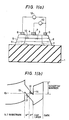
- FIG. 1(a) shows the structure of an FET which exploits the tunnel effect.
- This transistor basically has such a structure that, on a semi-insulating substrate crystal 1, a very thin layer having a p+/n+ homo-junction (2, 3) which has a band gap smaller than that of the substrate and whose whole thickness is equal to the width of a depletion layer or so is formed, and that it is held in a double heterojunction defined by the substrate crystal 1 and a cap layer 4 which has a band gap greater than that of this layer having the p+/n+ junction (2, 3).
- the p+-layer 2 and n+-layer 3 are respectively formed with contact regions 6 and 5 by diffusion, ion implantation or the like, and a drain electrode 9 and a source electrode 8 are formed on the respective contact regions.
- a gate electrode 7 is formed on the cap layer 4.
- Numerals 12 and 13 in the figure indicate a source - drain bias (V sd ) and a gate bias (V g ), respectively.
- a two-dimensional electron gas layer 10 or 14 and a two-dimensional hole gas layer 11 or 15 are induced at the heterojunction boundaries of the double heterojunction structure, and the charges of these layers balance with the total quantities of the charges of ionized donors 16 and ionized acceptors 17 within the depletion layer of the p+/n+ junction, whereby an electrical neutral condition is held.
- the two-dimensional electron gas 10 or 14 and the two-dimensional hole gas 11 or 15 join with the source electrode 8 in Fig. 1(a) and with the drain electrode 9 in the same under very low series resistances, respectively.
- the source - drain bias V sd and the gate bias V g are respectively applied to the source electrode 8 and the gate electrode 7 with reference to the drain electrode 9 as illustrated in Fig. 1(a).
- Fig. 2(a) illustrates a situation in which a reverse tunneling current flows under a reverse bias
- FIG. 2(b) illustrates a situation in which a forward tunneling current flows.
- the reverse bias when the gate voltage is enlarged, the current increases monotonically, but with a forward bias, when the gate voltage is enlarged, decrease in the tunneling current occurs on the basis of the same principle as in the Esaki diode.
- Such currents I sd do not depend very intensely upon the source - drain voltages V sd .
- the speed at which the tunneling arises is on the order of picoseconds, so that a switching time of about 100 picoseconds can be achieved by optimalizing the capacity and current value of the device.
- leakage currents can develop through the p-n junctions between the n+-layer 3 and p+-contact layer 4 and between the p+-layer 2 and the n+-contact layer 5.
- the influences of the leakage currents are negligibly small.
- the width of the depletion layer is approximately 100 ⁇
- the internal electric field is approximately 1 ⁇ 106 V/cm
- the sum of the thicknesses of the p+-layer and the n+-layer may be 100 ⁇ - 150 ⁇ .
- the peak current density J p corresponding to the peak current I p of the tunnel diode stated before is approximately 102 A/cm2.
- Fig. 7 shows another embodiment of the present invention. This embodiment is an improvement on the embodiment of Fig. 1(a). Although the leakage current between the source and drain is negligible in the embodiment of Fig. 1(a), it is more reduced to enhance characteristics in the present embodiment.
- a buffer layer 71 is formed on a substrate crystal 82, and that a layer having a p+/n+ homo-junction (72, 73) which has a band gap smaller than that of the buffer layer 71 and which has a whole thickness nearly equal to the width of a depletion layer is so formed as to be held in a double heterojunction defined by the buffer layer 71 and a cap layer 74 which has a band gap greater than that of the layer having the p+/n+ junction (72, 73).
- an ion-implanted layer (n++) 75 is formed on the side of a source electrode 78 by, for example, the ion implantation of Si so shallowly that the n+/p+ boundary is not reached, while the cap layer 74 and the n+-layer 73 on the side of a drain electrode 79 are etched and removed down to the n+/p+ boundary by dry etching, and a p+-layer 76 is formed in the corresponding part of the p+-layer 72 by the diffusion of Zn or the ion implantation of Be.
- ohmic electrodes are respectively formed on the n++-layer 75, p++-layer 76 and cap layer 74 as the source electrode 78, the drain electrode 79 and a gate electrode 77 by evaporation.
- the leakage current elucidated in Figs. 1(a) and 1(b) is almost null, and hence, a semiconductor device of still better characteristics can be realized.
- the first semiconductor layer defined in the present invention is the buffer layer 71 formed on the crystal substrate 82.
- Such a construction may of course be employed.
- GaAs substrate it is possible to use Ga 1-x Al x As for the buffer layer, a GaAs-based material for the third semiconductor layer, and Ga 1-u Al u As ( u ⁇ 0.3) for the second semiconductor layer.
- InP substrate it is possible to use InP, InAlAs or InGaAsP for the buffer layer, InGaAs or InGaAsP for the third semiconductor layer, and InAlAs, InGaAsP or InGaAlAs for the second semiconductor layer.
- a semi-insulating material is suitable as the substrate 82.
- FIG. 3 shows another example of a crystal structure which the semiconductor device according to the present invention possesses.
- a substrate 31 was semi-insulating GaAs, on which a p+/n+ junction layer made up of p+-Ge (p ⁇ 1 ⁇ 1018 - 1019 cm ⁇ 3, thickness ⁇ 100 ⁇ ) 32 and n+-Ge (n ⁇ 1 ⁇ 1018 - 1019 cm ⁇ 3, thickness ⁇ 100 ⁇ ) 33, and a hetero-cap layer 34 (undoped GaAs or Al x Ga 1-x As ( x ⁇ 0.5 - 0.7), thickness: 500 - 2000 ⁇ ) were grown by molecular-beam epitaxy (MBE) or metal-organic chemical vapor deposition (MOCVD).
- MBE molecular-beam epitaxy
- MOCVD metal-organic chemical vapor deposition
- FIG. 4 shows still another example.
- a substrate 41 was semi-insulating InP
- a layer 42 was made of p+- In 0.53 Ga 0.47 As
- a layer 43 was made of n+-In 0.53 Ga 0.47 As (the total thickness of the layers 42 and 43 was approximately 100 ⁇ )
- a hetero-cap layer 44 was made of undoped InP or In 0.52 Al 0 .48 As (500 - 2000 ⁇ thick).
- a contact for the n+-layer was formed in such a way that a contact layer having an impurity concentration of or above 2 ⁇ 1018 cm ⁇ 3 was formed by a method of ion-implanting and then annealing Si, whereupon AnGe, Ni and An were evaporated and then alloyed as an ohmic electrode.
- the alloy layer was so deep as to penetrate the cap layer and to extend down to a level within the n+-layer.
- a contact for the p+-layer was formed in such a way that a contact layer was formed by diffusing Zn or ion-implating Be deep enough to reach the p+-layer, whereupon Cr-Au was or Ti, Pt and An were evaporated as an ohmic electrode.
- the parts of the layers other than device portions were mesa-etched and removed down to the substrate. Al/Ti, or the like was used as a gate metal.
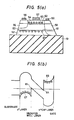
- a structure shown in Fig. 5(a) in which the barrier layer of a heterojunction was doped as in a HEMT, thereby to form a two-dimensional electron layer 60 and a two-dimensional hole layer 61 on both the sides of an undoped layer 53, and the tunneling between the layers 60 and 61 was controlled by a gate electrode 57. Since, in this case, the layer 53 was of high resistivity, the isolation between a source and a drain under the null gate voltage was improved. However, ohmic contacts for the two-dimensional electron and hole layers were more difficult than in the case of Fig. 1(a), and the parasitic resistance of an FET became high.
- a semi-insulating InP substrate 51 there were grown a p+-In 0.52 Al 0 .48 As layer 52 (1 ⁇ 1018 - 1019 cm ⁇ 3, 500 - 1000 ⁇ thick), the undoped In 0.53 Ga 0.47 As layer 53 (about 200 ⁇ thick), and an n+-In 0.52 Al 0.48 As layer 54 (1 ⁇ 1018 - 1019 cm ⁇ 3, 500 - 2000 ⁇ thick). With this crystal structure, characteristics similar to those of the structures in Figs. 3 and 4 were obtained.
- numerals 55 and 56 designate n-type and p-type contact layers, numerals 58 and 59 source and drain electrodes, and numerals 62 and 63 ionized doners and acceptors, respectively.
- numeral 64 indicates the two-dimensional electron gas layer, numeral 65 the two-dimensional hole gas layer, numeral 66 the ionized donors, and numeral 67 the ionized acceptors.
- the hetero-cap layer epitaxially grown on the p+/n+ junction layer was used.
- FET's in each of which the hetero-cap layer was replaced with an insulator gate such as of SiO2 or SiN x were fabricated for trial, and similar high-speed switching characteristics were attained.
- the FET in Fig. 1(a) had a very low series resistance, so that the thermal noise was of low level, and characteristics favorable for a high-frequency and low-noise transistor could be achieved.
Landscapes
- Junction Field-Effect Transistors (AREA)
Applications Claiming Priority (2)
| Application Number | Priority Date | Filing Date | Title |
|---|---|---|---|
| JP173649/86 | 1986-07-25 | ||
| JP61173649A JPH0783108B2 (ja) | 1986-07-25 | 1986-07-25 | 半導体装置 |
Publications (3)
| Publication Number | Publication Date |
|---|---|
| EP0256360A2 true EP0256360A2 (de) | 1988-02-24 |
| EP0256360A3 EP0256360A3 (en) | 1990-02-07 |
| EP0256360B1 EP0256360B1 (de) | 1993-11-24 |
Family
ID=15964526
Family Applications (1)
| Application Number | Title | Priority Date | Filing Date |
|---|---|---|---|
| EP87110764A Expired - Lifetime EP0256360B1 (de) | 1986-07-25 | 1987-07-24 | Steuerbare Tunneldiode |
Country Status (5)
| Country | Link |
|---|---|
| US (1) | US4835581A (de) |
| EP (1) | EP0256360B1 (de) |
| JP (1) | JPH0783108B2 (de) |
| CA (1) | CA1265626A (de) |
| DE (1) | DE3788253T2 (de) |
Cited By (10)
| Publication number | Priority date | Publication date | Assignee | Title |
|---|---|---|---|---|
| EP0521696A1 (de) * | 1991-07-01 | 1993-01-07 | Motorola, Inc. | Selbstdotierter, komplementärer Heteroübergangs-Feld-Effekt-Transistor hoher Leistung |
| EP0549373A1 (de) * | 1991-12-25 | 1993-06-30 | Nec Corporation | Tunneltransistor und dessen Herstellungsverfahren |
| EP0526897A3 (en) * | 1991-08-06 | 1993-08-11 | Nec Corporation | Three terminal tunnel device |
| DE4238545A1 (de) * | 1992-11-14 | 1994-05-19 | Daimler Benz Ag | Drucksensor und ein Verfahren zu dessen Herstellung |
| US5401980A (en) * | 1991-09-04 | 1995-03-28 | International Business Machines Corporation | 2D/1D junction device as a Coulomb blockade gate |
| EP0689250A1 (de) * | 1994-06-22 | 1995-12-27 | Kokusai Denshin Denwa Kabushiki Kaisha | Halbleiterbauelement mit einer Dreieckigen Sperrschichtdiodenstruktur |
| EP0853344A1 (de) * | 1996-12-27 | 1998-07-15 | Sanyo Electric Co. Ltd | Tunneleffekt-Halbleiteranordnung und Verfahren zur Herstellung |
| WO2004034475A1 (ja) * | 2002-10-09 | 2004-04-22 | Matsushita Electric Industrial Co., Ltd. | プラズマ振動スイッチング素子 |
| WO2008041188A1 (en) * | 2006-10-05 | 2008-04-10 | Nxp B.V. | Tunnel field effect transistor |
| GB2482308A (en) * | 2010-07-28 | 2012-02-01 | Univ Sheffield | Super junction silicon devices |
Families Citing this family (16)
| Publication number | Priority date | Publication date | Assignee | Title |
|---|---|---|---|---|
| FR2619250B1 (fr) * | 1987-08-05 | 1990-05-11 | Thomson Hybrides Microondes | Transistor hyperfrequence a double heterojonction |
| US5172194A (en) * | 1987-09-16 | 1992-12-15 | National Science Council | Structures of modulation doped base hot electron transistors |
| US6253307B1 (en) | 1989-05-04 | 2001-06-26 | Texas Instruments Incorporated | Data processing device with mask and status bits for selecting a set of status conditions |
| US5313117A (en) * | 1991-07-22 | 1994-05-17 | Nippon Telegraph And Telephone Corporation | Semiconductor logic circuit using two n-type negative resistance devices |
| US6617643B1 (en) | 2002-06-28 | 2003-09-09 | Mcnc | Low power tunneling metal-oxide-semiconductor (MOS) device |
| US7026642B2 (en) * | 2003-08-27 | 2006-04-11 | Micron Technology, Inc. | Vertical tunneling transistor |
| JP4840056B2 (ja) * | 2006-09-29 | 2011-12-21 | Toto株式会社 | 水栓及びその取付方法 |
| US8436422B2 (en) * | 2010-03-08 | 2013-05-07 | Sematech, Inc. | Tunneling field-effect transistor with direct tunneling for enhanced tunneling current |
| US8421165B2 (en) | 2010-05-11 | 2013-04-16 | Sematech, Inc. | Apparatus, system, and method for tunneling MOSFETs using self-aligned heterostructure source and isolated drain |
| US8586993B2 (en) | 2012-02-28 | 2013-11-19 | Infineon Technologies Austria Ag | Normally-off compound semiconductor tunnel transistor |
| US20140090684A1 (en) * | 2012-09-24 | 2014-04-03 | Joshua R. Smith | Heterojunction electrode with two-dimensional electron gas and surface treatment |
| CN105247682B (zh) * | 2013-06-27 | 2019-01-22 | 英特尔公司 | 具有未掺杂的漏极未覆盖环绕区的隧穿场效应晶体管(tfet) |
| TWI555209B (zh) * | 2013-07-29 | 2016-10-21 | 高效電源轉換公司 | 具有降低的輸出電容之氮化鎵裝置及其製法 |
| KR101515071B1 (ko) * | 2013-11-29 | 2015-04-24 | 가천대학교 산학협력단 | 실리콘 집적가능한 게르마늄 기반의 높은 정공이동도를 갖는 트랜지스터 |
| US9768311B2 (en) | 2014-07-24 | 2017-09-19 | Ecole Polytechnique Federale De Lausanne (Epfl) | Semiconductor tunneling device |
| CN104241375B (zh) * | 2014-08-29 | 2017-03-22 | 北京大学 | 一种跨骑型异质结共振隧穿场效应晶体管及其制备方法 |
Family Cites Families (11)
| Publication number | Priority date | Publication date | Assignee | Title |
|---|---|---|---|---|
| US3462700A (en) * | 1966-08-10 | 1969-08-19 | Bell Telephone Labor Inc | Semiconductor amplifier using field effect modulation of tunneling |
| DE2913068A1 (de) * | 1979-04-02 | 1980-10-23 | Max Planck Gesellschaft | Heterostruktur-halbleiterkoerper und verwendung hierfuer |
| DE3279663D1 (en) * | 1981-06-17 | 1989-06-01 | Hitachi Ltd | Heterojunction semiconductor device |
| US4538165A (en) * | 1982-03-08 | 1985-08-27 | International Business Machines Corporation | FET With heterojunction induced channel |
| JPS59111371A (ja) * | 1982-12-16 | 1984-06-27 | Nippon Telegr & Teleph Corp <Ntt> | 電界効果トランジスタ |
| JPH0654784B2 (ja) * | 1984-06-11 | 1994-07-20 | 沖電気工業株式会社 | 半導体装置 |
| JPS60263471A (ja) * | 1984-06-11 | 1985-12-26 | Oki Electric Ind Co Ltd | 半導体装置 |
| US4686550A (en) * | 1984-12-04 | 1987-08-11 | American Telephone And Telegraph Company, At&T Bell Laboratories | Heterojunction semiconductor devices having a doping interface dipole |
| JPS61147577A (ja) * | 1984-12-21 | 1986-07-05 | Toshiba Corp | 相補型半導体装置 |
| JPS61174776A (ja) * | 1985-01-30 | 1986-08-06 | Sony Corp | ヘテロ接合電界効果トランジスタ |
| CA1256590A (en) * | 1985-03-15 | 1989-06-27 | Yuichi Matsui | Compound semiconductor device with layers having different lattice constants |
-
1986
- 1986-07-25 JP JP61173649A patent/JPH0783108B2/ja not_active Expired - Lifetime
-
1987
- 1987-07-22 CA CA000542705A patent/CA1265626A/en not_active Expired
- 1987-07-23 US US07/076,765 patent/US4835581A/en not_active Expired - Fee Related
- 1987-07-24 EP EP87110764A patent/EP0256360B1/de not_active Expired - Lifetime
- 1987-07-24 DE DE87110764T patent/DE3788253T2/de not_active Expired - Fee Related
Cited By (18)
| Publication number | Priority date | Publication date | Assignee | Title |
|---|---|---|---|---|
| EP0521696A1 (de) * | 1991-07-01 | 1993-01-07 | Motorola, Inc. | Selbstdotierter, komplementärer Heteroübergangs-Feld-Effekt-Transistor hoher Leistung |
| EP0526897A3 (en) * | 1991-08-06 | 1993-08-11 | Nec Corporation | Three terminal tunnel device |
| US5686739A (en) * | 1991-08-06 | 1997-11-11 | Nec Corporation | Three terminal tunnel device |
| US5401980A (en) * | 1991-09-04 | 1995-03-28 | International Business Machines Corporation | 2D/1D junction device as a Coulomb blockade gate |
| EP0549373A1 (de) * | 1991-12-25 | 1993-06-30 | Nec Corporation | Tunneltransistor und dessen Herstellungsverfahren |
| US5705827A (en) * | 1991-12-25 | 1998-01-06 | Nec Corporation | Tunnel transistor and method of manufacturing same |
| DE4238545A1 (de) * | 1992-11-14 | 1994-05-19 | Daimler Benz Ag | Drucksensor und ein Verfahren zu dessen Herstellung |
| EP0689250A1 (de) * | 1994-06-22 | 1995-12-27 | Kokusai Denshin Denwa Kabushiki Kaisha | Halbleiterbauelement mit einer Dreieckigen Sperrschichtdiodenstruktur |
| EP0853344A1 (de) * | 1996-12-27 | 1998-07-15 | Sanyo Electric Co. Ltd | Tunneleffekt-Halbleiteranordnung und Verfahren zur Herstellung |
| WO2004034475A1 (ja) * | 2002-10-09 | 2004-04-22 | Matsushita Electric Industrial Co., Ltd. | プラズマ振動スイッチング素子 |
| US6953954B2 (en) | 2002-10-09 | 2005-10-11 | Matsushita Electric Industrial Co., Ltd. | Plasma oscillation switching device |
| CN1332453C (zh) * | 2002-10-09 | 2007-08-15 | 松下电器产业株式会社 | 等离子体振动开关元件 |
| WO2008041188A1 (en) * | 2006-10-05 | 2008-04-10 | Nxp B.V. | Tunnel field effect transistor |
| US7839209B2 (en) | 2006-10-05 | 2010-11-23 | Nxp B.V. | Tunnel field effect transistor |
| GB2482308A (en) * | 2010-07-28 | 2012-02-01 | Univ Sheffield | Super junction silicon devices |
| WO2012013943A1 (en) * | 2010-07-28 | 2012-02-02 | The University Of Sheffield | Semiconductor devices with 2deg and 2dhg |
| US9087889B2 (en) | 2010-07-28 | 2015-07-21 | The University Of Sheffield | Semiconductor devices with 2DEG and 2DHG |
| EP3876290A3 (de) * | 2010-07-28 | 2021-12-15 | The University of Sheffield | Halbleitervorrichtungen |
Also Published As
| Publication number | Publication date |
|---|---|
| DE3788253D1 (de) | 1994-01-05 |
| DE3788253T2 (de) | 1994-03-17 |
| EP0256360B1 (de) | 1993-11-24 |
| JPH0783108B2 (ja) | 1995-09-06 |
| CA1265626A (en) | 1990-02-06 |
| US4835581A (en) | 1989-05-30 |
| JPS6331173A (ja) | 1988-02-09 |
| EP0256360A3 (en) | 1990-02-07 |
Similar Documents
| Publication | Publication Date | Title |
|---|---|---|
| EP0256360B1 (de) | Steuerbare Tunneldiode | |
| US5705827A (en) | Tunnel transistor and method of manufacturing same | |
| US5686739A (en) | Three terminal tunnel device | |
| EP0033876B1 (de) | Halbleitervorrichtung mit drei Anschlussklemmen | |
| KR100204688B1 (ko) | 헤테로 인터페이스를 가진 전계효과 트랜지스터 | |
| US4958208A (en) | Bipolar transistor with abrupt potential discontinuity in collector region | |
| EP0184827A2 (de) | Hochleistungstransistor hoher Geschwindigkeit | |
| EP0207968B1 (de) | Heisselektronen-unipolartransistor | |
| US4825265A (en) | Transistor | |
| JP2914049B2 (ja) | ヘテロ接合を有する化合物半導体基板およびそれを用いた電界効果トランジスタ | |
| US5949096A (en) | Field effect transistor with stabilized threshold voltage | |
| EP0566591A1 (de) | Halbleitervorrichtung. | |
| US4903091A (en) | Heterojunction transistor having bipolar characteristics | |
| US5049955A (en) | Semiconductor ballistic electron velocity control structure | |
| US4449140A (en) | Semi-conductor barrier switching devices | |
| EP0092645B1 (de) | Transistor und einen Transistor enthaltender Schaltkreis | |
| EP1083608B1 (de) | Feldeffekt-Halbleiteranordnung | |
| JP2643890B2 (ja) | トンネルトランジスタ | |
| EP0361759A2 (de) | Heterostrukturbipolartransistor | |
| JP2695832B2 (ja) | ヘテロ接合型電界効果トランジスタ | |
| JPH07263708A (ja) | トンネルトランジスタ | |
| EP0278110B1 (de) | Feldeffekttransistor mit Heteroübergang | |
| KR920002092B1 (ko) | 매립형 쇼트키 전극을 이용한 고속 수광소자 | |
| JP2861590B2 (ja) | トンネルトランジスタ | |
| JPH0620076B2 (ja) | ヘテロ接合バイポーラトランジスタ |
Legal Events
| Date | Code | Title | Description |
|---|---|---|---|
| PUAI | Public reference made under article 153(3) epc to a published international application that has entered the european phase |
Free format text: ORIGINAL CODE: 0009012 |
|
| AK | Designated contracting states |
Kind code of ref document: A2 Designated state(s): DE FR GB |
|
| PUAL | Search report despatched |
Free format text: ORIGINAL CODE: 0009013 |
|
| AK | Designated contracting states |
Kind code of ref document: A3 Designated state(s): DE FR GB |
|
| 17P | Request for examination filed |
Effective date: 19900427 |
|
| 17Q | First examination report despatched |
Effective date: 19911014 |
|
| GRAA | (expected) grant |
Free format text: ORIGINAL CODE: 0009210 |
|
| AK | Designated contracting states |
Kind code of ref document: B1 Designated state(s): DE FR GB |
|
| REF | Corresponds to: |
Ref document number: 3788253 Country of ref document: DE Date of ref document: 19940105 |
|
| ET | Fr: translation filed | ||
| PLBE | No opposition filed within time limit |
Free format text: ORIGINAL CODE: 0009261 |
|
| STAA | Information on the status of an ep patent application or granted ep patent |
Free format text: STATUS: NO OPPOSITION FILED WITHIN TIME LIMIT |
|
| 26N | No opposition filed | ||
| PGFP | Annual fee paid to national office [announced via postgrant information from national office to epo] |
Ref country code: FR Payment date: 19970721 Year of fee payment: 11 |
|
| PGFP | Annual fee paid to national office [announced via postgrant information from national office to epo] |
Ref country code: DE Payment date: 19970925 Year of fee payment: 11 |
|
| PGFP | Annual fee paid to national office [announced via postgrant information from national office to epo] |
Ref country code: GB Payment date: 19980624 Year of fee payment: 12 |
|
| PG25 | Lapsed in a contracting state [announced via postgrant information from national office to epo] |
Ref country code: FR Free format text: LAPSE BECAUSE OF NON-PAYMENT OF DUE FEES Effective date: 19990331 |
|
| PG25 | Lapsed in a contracting state [announced via postgrant information from national office to epo] |
Ref country code: DE Free format text: LAPSE BECAUSE OF NON-PAYMENT OF DUE FEES Effective date: 19990501 |
|
| REG | Reference to a national code |
Ref country code: FR Ref legal event code: ST |
|
| PG25 | Lapsed in a contracting state [announced via postgrant information from national office to epo] |
Ref country code: GB Free format text: LAPSE BECAUSE OF NON-PAYMENT OF DUE FEES Effective date: 19990724 |
|
| GBPC | Gb: european patent ceased through non-payment of renewal fee |
Effective date: 19990724 |