EP0256623B1 - Fassung für ein Gehäuse mit im Zickzack verlaufenden Anschlüssen - Google Patents
Fassung für ein Gehäuse mit im Zickzack verlaufenden Anschlüssen Download PDFInfo
- Publication number
- EP0256623B1 EP0256623B1 EP87304459A EP87304459A EP0256623B1 EP 0256623 B1 EP0256623 B1 EP 0256623B1 EP 87304459 A EP87304459 A EP 87304459A EP 87304459 A EP87304459 A EP 87304459A EP 0256623 B1 EP0256623 B1 EP 0256623B1
- Authority
- EP
- European Patent Office
- Prior art keywords
- portions
- cavities
- socket
- package
- row
- Prior art date
- Legal status (The legal status is an assumption and is not a legal conclusion. Google has not performed a legal analysis and makes no representation as to the accuracy of the status listed.)
- Expired - Lifetime
Links
Images



Classifications
-
- H—ELECTRICITY
- H05—ELECTRIC TECHNIQUES NOT OTHERWISE PROVIDED FOR
- H05K—PRINTED CIRCUITS; CASINGS OR CONSTRUCTIONAL DETAILS OF ELECTRIC APPARATUS; MANUFACTURE OF ASSEMBLAGES OF ELECTRICAL COMPONENTS
- H05K7/00—Constructional details common to different types of electric apparatus
- H05K7/02—Arrangements of circuit components or wiring on supporting structure
- H05K7/10—Plug-in assemblages of components, e.g. IC sockets
- H05K7/1015—Plug-in assemblages of components, e.g. IC sockets having exterior leads
- H05K7/103—Plug-in assemblages of components, e.g. IC sockets having exterior leads co-operating by sliding, e.g. DIP carriers
- H05K7/1038—Plug-in assemblages of components, e.g. IC sockets having exterior leads co-operating by sliding, e.g. DIP carriers with spring contact pieces
Definitions
- the instant invention relates to a socket for mounting to a printed circuit board and for interconnecting the leads of an integrated circuit in the configuration of a zig-zag inline package to the traces on the printed circuit board.
- U.S. Patent 4,060,296 a carrier for interconnecting thereto a dual inline package integrated circuit.
- the disclosure of the above-referenced U.S. patent shows dual leaf contacts mounted within a carrier cavity. Dual leaf refers to the mating configuration between the contact leaves and the package lead, in that there is metal-to-metal contact between the package lead and the socket contact, on both sides of the package lead.
- the dual inline package carrier as disclosed in U.S. Patent 4,060,296, however, was designed for DIP packages having leads with lateral spacing on 2,54 mm (0.100 inch) centerlines, and 7,62 mm (0.300 inch) width between the opposed leads.
- a DIP package consists of package leads extending outwardly from sidewalls of the package, then bending downwardly. As the radius in the lead is at the package body, the DIP lead can handle at least 500 grams of insertion force before overstressing the DIP leads.
- the zig-zag inline package body is similar in design to that of the dual inline package, the major difference lies in the lead configuration.
- the zig-zag inline package leads extend from one side of the package only, every other lead being bent away from the axial centerline in the opposite direction forming two axial rows of leads.
- the leads on the zig-zag inline package in the same axial row have 2,54 mm (0.100 inch) centerlines, each lead being laterally offset 1,27 mm (.050 inch) from the next offset lead.
- the distance between axial rows is now 2,54 mm (.100 inch), as opposed to 7,62 mm (.300 inch) on the dual inline package.
- the leads on the zig-zag inline package extend downwardly from the package, are then formed by a first radius projecting the lead outward away from the axial centerline of the package, and then by a second radius bending the lead back towards the axial centerline until the leads are again extending downwardly.
- the leads of the zig-zag inline package are extremely sensitive to overstress at the first and second radius, overstressing at approximately 270 grams insertion force.
- the socket configuration disclosed in U.S. Patent 4,060,296 could not be utilized for the zig-zag inline package.
- the disclosure of the above-mentioned patent relates to the interconnections for square matrix packages whereas the zig-zag inline package has an offset configuration, Furthermore, as the socket contacts are laterally opposed, the distance between axial rows of contacts was 0.300 inch, and could not be reduced to 0.100 inch with the contact directly opposed.
- the contacts as disclosed in the above-mentioned patent could not be utitized for the zig-zag inline package, as the insertion force on those contacts were not predictable enough to consistently maintain below a 270 gram insertion force.
- the contacts disclosed in U.S. Patent 4,060,296 were formed with the two leaves in contact in a preloaded configuration. As the insertion force is directly related to the contact leaf preload, and as the contact leaf preload cannot be consistently held, the insertion force could not be held consistently either.
- the first objective is accomplished by providing a housing with a plurality of contact receiving cavities in parallel but offset rows, and contacts disposed in the cavities providing contact portions to both the integrated circuit package lead and the printed circuit board.
- the second objective is accomplished by stamping and forming the electrical contacts such that no preload exists in the integrated circuit package lead contacting portion.
- the contact is dimensionally controlled to be biased to a preloaded condition only when inserted in the housing.
- the third object is accomplished by providing standoffs projecting from the package receiving face integral with the housing to accurately locate the package leads within the contacts and prevent further insertion.
- the fourth objective is accomplished by abutting the end cavities of adjacent cavities in adjacent sockets to keep the centerline spacing of adjacent cavities equal to the lateral spacing between adjacent cavities in the same socket.
- the present invention consists in an electrical socket as defined in claim 1.
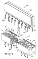
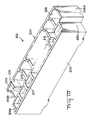
- the socket 2 of the preferred embodiment poised for receiving a zig-zag inline package 100.
- the socket 2 comprises a socket housing 4 and a plurality of contacts 50 mounted therein.
- a zig-zag inline package 100 having a body 102 and leads 104, 104'.
- the leads 104, 104' all extend downwardly from wall 112, leads 104, 104' on the same axial centerline.
- the package lead 104 extends downwardly and is then bent outwardly away from the axial centerline at radius 106.
- the lead projects outwardly to a second radius 108 where the lead is bent back towards the axial centerline and extends downwardly as straight section 110.
- Lead 104' is bent in the same fashion as lead 104 at first and second radius 106', 108', but in the opposite direction in relation to the axial centerline.
- a typical zig-zag inline package which is commercially available is the Mitsubishi 256K DRAM, number MJM4256L-12.
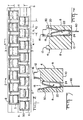
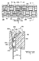
- the socket 2 includes a first and second row of contacts 50, the first row being laterally offset from the second row along the axial centerline, the first and second row of contacts 50 being spaced as the package leads 104, 104'.
- the distance Y attainable between rows of contacts, in the preferred embodiment is 2,54 mm (0.100 inches).
- the lateral offset between the two rows, X1, is 1,27 mm (0.050 inches) and the centerline spacing between contacts in the same row, X2, is also 2,54 mm (0.100 inches).
- the socket 2 is shown as having a housing 4 including endwalls 6, sidewalls 8, a bottom wall 10, an upper face 12, and a package receiving face 18. Extending from the bottom wall 10 are lower standoffs 14, and extending upwardly from the upper face 12 are upper standoffs 16.
- the socket housing 4 further comprises a plurality of contact receiving cavities 20.
- Cavities 20 are defined by a floor 34, outer sidewalls 22, inner sidewalls 24, and endwalls 26.
- the contact lead-in portion of cavity 20 is defined by outer beveled surfaces 28, inner beveled surfaces 30, and end beveled surfaces 32.
- At the bottom of the cavity 20 and extending through the floor 34 are apertures 36 having lead-in surfaces 38, 40 therearound. It should be noticed that a lead-in surface 42 is located between the outer sidewalls 22 and the floor 34, and is continuous with lead in surface 40.
- Contact 50 is shown exploded away from the connector body 4 and the cavity 20, and shown inserted in the cavity in phantom.
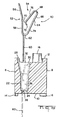
- Contact 50 includes a first and second leaf section 52, 54, respectively, and a printed circuit board lead section 60.
- Contact 50 is stamped and formed from flat metal stock.
- the first leaf section comprises a lead-in section 56 and a straight section 58.
- the printed circuit board contact 60 is stamped from the central portion of the contact 50, and is then bent downwardly, as best shown in Figures 1 and 6.
- Second leaf portion 54 begins with the stamping being bent at a first radius 62 projecting the stamping upwardly in the same direction as the first leaf portion 52, along a straight leg portion 74.
- the stamping has a portion 66 bent away from the straight portion 74, about a corner 64.
- the stamping is then again formed about a second radius 68, which projects the contact portion 70 inwardly towards the first leaf portion 52.
- the second leaf portion 54 Upon insertion of the contact 50 into the cavity 20, the second leaf portion 54 is brought forward into contact with the first leaf portion 52.
- the first and second leaves are centered in the cavity by beveled surfaces 28, 30 and 32.
- the straight portion 58 of the contact then lies adjacent to the outer cavity sidewall, the two surfaces in sliding relation with one another.
- Further insertion of the contact 50 causes portion 74 of contact 50 to interfere with the inner beveled surface 30, and continued insertion causes beveled surface 30 to act as a camming surface, projecting the second leaf portion 54 into the first leaf portion 52.
- the contacts 50 are held in place within the cavity by the lances 78 ( Figure 1) sciving into the sidewalls 26 upon insertion.
- the printed circuit board contact 60 will follow beveled surface 28, outer sidewall 22, sidewall beveled surface 42 and into the aperture 36 As the contacts are mass inserted on carrier strips, it is important for the cavity to be designed to allow entry of the contact portion 60 and centering of the contact portion 60 into the aperture.
- the fit between the contact portion 60 and the aperture 36 is an interference fit, thereby sealing the interior part of the cavity from the printed circuit board side of the housing. As the connector 2 will eventually be soldered to a printed circuit board, the sealing feature of the aperture 36 will prevent solder and flux from wicking into the cavities 20.
- the contact lead-in section 56 lies adjacent to surface 28
- straight portion 58 lies adjacent to outer cavity sidewall 22
- section 66 lies adjacent to inner beveled surface 30, as shown in Figure 6.
- the second radius 68 of contact 50 is larger than it could have been, had the sidewall 24 not contained the bevel 30, but rather, had continued as a straight wall.
- the lead-in section 56 and section 76 form an opening for a lead of a zig-zag inline package, and contact portion 70 is biased against portion 58 with a predetermined preload.
- the stamped configuration of the contact 50 in its free state is accurately held geometrically and as the contact cavity 50 is also dimensionally controlled, the deformation of the contact 50, upon insertion into the cavity 20, creates a predictable preload between the first and second leaf portions 52, 54, respectively.
- the insertion force is a function of the preload and the coefficient of friction between the package leads and the leaf sections of the contact, the insertion force of the package may also be consistently maintained.
- the connector 2 may then be installed on the printed circuit board for receipt of a package.
- the connector 2 is placed on the printed circuit board 130 with the contact portions 60 extending through the printed circuit board through holes 134 and the contact portions 60 soldered to the individual traces 132, as shown in Figure 7.
- the package leads 110, 110' are aligned with the openings formed by the contact sections 56 and 76.
- the insertion force required to insert the package 100 is designed to be less than 270 grams, as the package leads at 106, 106', 108, 108' will overstress at approximately 270 grams.
- standoff portions 16 are included above the upper face 12, such that the package sidewall 112 bottoms out on the standoff 16. As most integrated circuit packages are robotically assembled in a pick and place mode, the robot will sense the interference between the standoff 16 and the package 100. If the package 100 was inserted into the connector 2 without the standoffs, the ends of leads 110, 110' could bottom out against the contacts and be damaged before the robot sensed the resistance.
- the instant design allows the continuity of the solder joint between the individual contacts 50 and the printed circuit board traces 132 to be tested.
- probing instruments may be inserted under the package 100 and above the connector 2 for probing against the contacts 50.
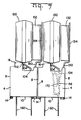
- the instant invention may also include an integral decoupling capacitor, as shown in Figure 7.
- An integrated circuit package is decoupled from the power source for two purposes. First, when several integrated circuit packages demand power at the same time, the voltage in the power supply will drop because the power source cannot supply enough current to maintain the voltage. The capacitor will have enough electrical charge stored up to make up the difference and keep the integrated circuit packages operating. Secondly, when integrated circuit packages go through the refresh cycle, the voltage will change so rapidly that it will cause a spike in the power supply, and the capacitor will filter out those spikes.
- the capacitor 152 is formed integrally with the contact portions 150, the capacitor being vapor phase soldered onto the contact portions 150.
- the contact portions 150 has the same constituent components as the contact portions 50, rather, instead of being sheared off at the height of the upper face 12, the contacts 150 include capacitor mounting faces 154.
- the contacts 150 can be formed in carrier strip form and robotically inserted.
- a typical capacitor for decoupling an integrated circuit package is a .33 micro-farad, multi-layer ceramic capacitor manufactured by AVX, Inc.
- one of the contact portions 150 is located at the power lead of the package and one contact portion 150 is located at the ground lead of the integrated circuit package.
- the instant invention further saves printed circuit board space, in that the capacitor does not have to be mounted directly on the printed circuit board, which, heretofore has been the practice.
- the addition of the decoupling capacitor to the contact portions 150 does not increase the side-by-side stacking clearance of the package sockets.
- the center-to-center spacing of the adjacent contacts in adjacent connectors can be maintained at 0.100 inches, as shown in Figure 9 as Z.
- FIG 10 An alternative embodiment is shown in Figure 10, which allows the sockets to be stacked end-to-end, maintaining the same center-to-center spacing between the adjacent contacts of adjacent sockets as the center-to-center spacing of adjacent contacts in the same socket.
- the housings 202 can be stacked end-to-end and still maintain the distance T between adjacent contacts of 2,54 mm (0.100 inches), as shown in Figure 11.
- the distance X3 between adjacent contacts in the same socket is also 2,54 mm (0.100 inches).
- the alternative embodiment employs a design similar to that of the preferred embodiment except for the design of the endwalls 206 and the location of the package standoffs 216.
- the alternate embodiment includes endwalls 206a laterally offset from endwalls 206b, and endwalls 206c laterally offset from endwalls 206d. This lateral offset allows the endwalls 206a, 206b of the adjacent connector to abut endwalls 206c, 206d respectively, maintaining the same center-to-center distance between adjacent cavities of adjacent connectors as adjacent cavities in the same connector.
- the design of the cavities 220 must be modified. As shown in Figure 10, the package standoffs 216 are moved to the interior portion of the connector housing 204. Also, as shown in Figure 12, the interior sidewall 230 must be modified by returning to a vertical portion 231 above the contact location. Otherwise, the sidewall portion 230 would become too thin at the upper edge for molding.
- the vertical section 231 does not affect the performance of the contact, as the vertical section begins at the tangency point of the contact second radius 68 and the interior sidewall 230.
Landscapes
- Engineering & Computer Science (AREA)
- Microelectronics & Electronic Packaging (AREA)
- Coupling Device And Connection With Printed Circuit (AREA)
- Connecting Device With Holders (AREA)
Claims (7)
- Elektrische Steckleiste (2, 202) zum elektrischen Anschließen eines integrierten Schaltkreis-Gehäuses (100), wobei das Gehäuse (100) einen Körperteil (102) und einen Leiter-Rahmenteil mit einer Vielzahl von Leitern (104, 104') aufweist, die sich alle von einem Seitenrand (112) des Körperteils (102) aus erstrecken, wobei die Leiter (104, 104') zu zwei parallelen Reihen mit jedem zweiten Leiter in versetzter Anordnung geformt sind, die Steckleiste (2, 202) über ein Isoliergehäuse (4, 204) mit sich axial erstreckenden Seitenwänden (8, 208), Stirnwänden (6) und zwei parallelen Reihen von Kontakt-Aufnahmehohlräumen (20, 220) verfügt, die in eine obere Gehäuse-Aufnahmefläche (18) münden, wobei jede Steckleiste (2, 202) des weiteren über einen elektrischen Anschluß (50) zum Anschließen an den Gehäuseleitern (104, 104') verfügt, die Anschlüsse (50) einander gegenüberliegende Kontaktabschnitte (58, 70) aufweisen, das Gehäuse (4, 204) vorstehende Teile (16, 216) an der Gehäuse-Aufnahmefläche (18) und von dieser sich nach außen erstreckend aufweist und des weiteren eine zentrale Stützrippe (5, 205) aufweist, die sich entlang der axialen Mittellinie erstreckt, wobei jede Reihe der Hohlräume (20, 220) an einander gegenüberliegenden Seiten der zentralen Stützrippe (5, 205) vorgesehen ist, die Hohlräume (20, 220) in einer ersten Reihe gegenüber den Hohlräumen (20, 220) in einer zweiten Reihe axial versetzt sind, wobei die seitlichen Mittellinien der Hohlräume (20, 220) in der ersten Reihe in gleichen Abständen zwischen den seitlichen Mittellinien der benachbarten Hohlräume (20, 220) in der zweiten Reihe angeordnet sind, die Hohlräume (20, 220) des weiteren durch Hohlraumwände (26, 226) begrenzt sind, die quer zu der zentralen Stützrippe (5, 205) verlaufen und seitlich in Abständen angeordnet sind, um die versetzten Hohlräume (20, 220) zu begrenzen, der Umfang jedes Hohlraums (20, 220) durch einen Boden (34, 234) mit einer sich durch diesen hindurch erstreckenden Öffnung (36, 236) und durch eine Innenfläche (24, 224) als Teil der zentralen Stützrippe (5, 205) begrenzt ist, die sich von dem Boden (34, 234) nach oben erstreckt, wobei der Hohlraumumfang des weiteren eine Außenfläche (22, 222) als Teil der Seitenwand (8, 208) aufweist, die sich von dem Boden (34, 234) nach oben und im wesentlichen rechtwinklig hierzu erstreckt, wobei die Außenfläche (22, 222) in eine äußere Schrägfläche (28, 228) als Teil der Seitenwand (8, 208) übergeht, die von der axialen Mittellinie des Gehäuses (4, 204) aus vorspringt, wobei die Anschlüsse (50) erweiterte Abschnitte (56) aufweisen, die bündig mit den äußeren Schrägflächen (28, 228) verlaufen, wobei die erweiterten Abschnitte (56) in erste Kontaktabschnitte (58) übergehen, die in der Nähe der äußeren Schrägflächen (28) angeordnet sind, die ersten Kontakabschnitte (58) in erste rückwärts umgebogene Abschnitte (62) in der Nähe des Bodens (34) und in dahinter liegende Anschlußabschnitte (74) übergehen, die sich nach oben und in zweite rückwärts umgebogene Abschnitte (68) erstrecken, von denen sich diagonale Abschnitte (76) nach unten und in zweite Kontaktabschnitte (70) erstrecken, die gegen jeweilige erste Kontaktabschnitte (58) vorgespannt sind, wobei die sich nach oben erstreckenden Anschlußabschnitte (74) diagonal innerhalb der Hohlräume (20, 220) von den ersten Kontaktabschnitten (58) aus weg angeordnet sind, um die zweiten rückwärts umgebogenen Abschnitte (68) in einem Abstand von dort anzuordnen, wobei die Anschlüsse (50) des weiteren über Endabschnitte (60) verfügen, die sich nach unten erstrecken und durch die Öffnungen (36, 236) im Boden (34, 234) zum Anschluß an einer gedruckten Schaltungsplatte vorstehen.
- Steckleiste (2, 202) nach Anspruch 1, dadurch gekennzeichnet, daß die Innenflächen (24, 224) in innere Schrägflächen (30, 230) als Teil der zentralen Stützrippe (5, 205) übergehen, welche Schrägflächen in Richtung auf die axiale Mittellinie des Gehäuses (4, 204) vorstehen, wobei der Schnitt der Innenflächen (24, 224) und der inneren Schrägflächen (30, 230) Ecken (46, 246) bildet.
- Steckleiste (2, 202) nach Anspruch 2, dadurch gekennzeichnet, daß die sich nach oben erstreckenden Anschlußabschnitte (74) innerhalb der Hohlräume (20, 220) derart angeordnet sind, daß die sich nach oben erstreckenden Anschlußabschnitte (74) in einer Kontaktbeziehung mit den Ecken (46, 246) stehen.
- Steckleiste (2, 202) nach Anspruch 3, dadurch gekennzeichnet, daß die sich nach oben erstreckenden Anschlußabschnitte (74) in der Nähe der Ecken (46, 246) in Richtung auf die inneren Schrägflächen (30, 230) umgebogen sind, wodurch der Winkel zwischen den erweiterten Abschnitten (56) und den diagonalen Abschnitten (76) vergrößert ist.
- Steckleiste (2, 202) nach Anspruch 1, dadurch gekennzeichnet, daß das Gehäuse (204) zum endseitigen Stapeln profiliert ist, wobei der Axialabstand zwischen benachbarten Hohlräumen (220) benachbarter Verbinder gleich dem Axialabstand zwischen benachbarten Hohlräumen (220) bei demselben Verbinder ist, die Stirnwände (206a-206d) der Reihen der Hohlräume (220) wie die Hohlräume (220) versetzt sind, die Stirnwand (206c) in einer Reihe gegenüber der Stirnwand (206d) der anderen Reihe an einem ersten Ende des Gehäuses (204) axial zurückgezogen ist, während die Stirnwand (206b) der anderen Reihe gegenüber der Stirnwand (206a) der einen Reihe an einem zweiten Ende des Gehäuses (204) axial zurückgezogen ist.
- Steckleiste (2, 202) nach Anspruch 5, dadurch gekennzeichnet, daß die Stimwände (206a-206d) halb so dick wie die Hohlraumwände (207) zwischen benachbarten Hohlräumen (220) sind und daß ein Bereich der zentralen Stützrippe (205) zwischen den Stirnwänden der ersten und der zweiten Reihe (206a, 206b; 206c, 206d) an jedem Ende des Gehäuses (204) halb so dick wie der übrige Teil der zentralen Stützrippe (205) ist.
- Steckleiste (2, 202) nach Anspruch 6, dadurch gekennzeichnet, daß die inneren Schrägflächen (230) an einer Stelle in der Nähe der umgebogenen Abschnitte (68) in vertikale Flächen (231) übergehen, die sich zu der Gehäuse-Aufnahmefläche (18) hin erstrecken.
Applications Claiming Priority (2)
| Application Number | Priority Date | Filing Date | Title |
|---|---|---|---|
| US872740 | 1986-06-10 | ||
| US06/872,740 US4726776A (en) | 1986-06-10 | 1986-06-10 | Socket for zig-zag inline package |
Publications (2)
| Publication Number | Publication Date |
|---|---|
| EP0256623A1 EP0256623A1 (de) | 1988-02-24 |
| EP0256623B1 true EP0256623B1 (de) | 1993-09-01 |
Family
ID=25360216
Family Applications (1)
| Application Number | Title | Priority Date | Filing Date |
|---|---|---|---|
| EP87304459A Expired - Lifetime EP0256623B1 (de) | 1986-06-10 | 1987-05-20 | Fassung für ein Gehäuse mit im Zickzack verlaufenden Anschlüssen |
Country Status (4)
| Country | Link |
|---|---|
| US (1) | US4726776A (de) |
| EP (1) | EP0256623B1 (de) |
| JP (1) | JP2585603B2 (de) |
| DE (1) | DE3787237T2 (de) |
Families Citing this family (10)
| Publication number | Priority date | Publication date | Assignee | Title |
|---|---|---|---|---|
| US4820203A (en) * | 1988-01-14 | 1989-04-11 | Raychem Corporation | Multicontact connector |
| KR100260276B1 (ko) * | 1991-01-14 | 2000-07-01 | 윌리엄 비. 켐플러 | 수직 리드 온칩 패키지 |
| US5239199A (en) * | 1991-01-14 | 1993-08-24 | Texas Instruments Incorporated | Vertical lead-on-chip package |
| US5295869A (en) * | 1992-12-18 | 1994-03-22 | The Siemon Company | Electrically balanced connector assembly |
| JPH07176336A (ja) * | 1993-09-30 | 1995-07-14 | Siemon Co:The | ブレーク・テスト機能を含む電気的に拡張された配線ブロック |
| US5403195A (en) * | 1994-05-24 | 1995-04-04 | The Whitaker Corporation | Socket having an auxiliary electrical component mounted thereon |
| US6459042B1 (en) | 1999-12-17 | 2002-10-01 | Autoliv Asp, Inc. | Electrical connector with an electrical component holder |
| US6997750B2 (en) | 2003-07-23 | 2006-02-14 | Fci Americas Technology, Inc. | Electrical connector contact |
| US20110263163A1 (en) * | 2008-11-26 | 2011-10-27 | John Schmidli | Compact Multi-Contact Plug and Socket |
| CN110829069B (zh) * | 2018-11-01 | 2023-07-18 | 富士康(昆山)电脑接插件有限公司 | 连接器及其组合 |
Family Cites Families (15)
| Publication number | Priority date | Publication date | Assignee | Title |
|---|---|---|---|---|
| US848505A (en) * | 1903-06-18 | 1907-03-26 | Louis Steinberger | Interlocking terminal base. |
| US2724814A (en) * | 1952-09-04 | 1955-11-22 | Ilsco Copper Tube & Products I | Interlocking terminal block construction |
| US2855579A (en) * | 1955-09-28 | 1958-10-07 | Ind Hardware Mfg Co Inc | Socket for sub-miniature electronic device and manufacture of same |
| US4356532A (en) * | 1980-07-18 | 1982-10-26 | Thomas & Betts Corporation | Electronic package and accessory component assembly |
| US3880493A (en) * | 1973-12-28 | 1975-04-29 | Burroughs Corp | Capacitor socket for a dual-in-line package |
| US4060296A (en) * | 1976-10-26 | 1977-11-29 | Amp Incorporated | Low profile DIP receptacle |
| US4082408A (en) * | 1977-02-24 | 1978-04-04 | Gould, Inc. | Electric fuse holder |
| US4377319A (en) * | 1981-01-28 | 1983-03-22 | Amp Incorporated | Low insertion force dip connector |
| US4418974A (en) * | 1981-01-28 | 1983-12-06 | Amp Incorporated | Low insertion force socket assembly |
| US4606599A (en) * | 1981-12-17 | 1986-08-19 | Texas Instruments Incorporated | Low insertion force connector |
| US4428633A (en) * | 1982-03-01 | 1984-01-31 | Amp Incorporated | Dual-in-line socket assembly |
| US4478476A (en) * | 1982-04-19 | 1984-10-23 | Jones Elmer R | Dip burn-in socket |
| JPS58188184A (ja) * | 1982-04-27 | 1983-11-02 | 日本電気株式会社 | 金属芯入りプリント配線板の製造方法 |
| US4541034A (en) * | 1984-04-26 | 1985-09-10 | At&T Technologies, Inc. | Electrical terminal and method of securing same in circuit substrate thru-hole |
| JPS61194856A (ja) * | 1985-02-25 | 1986-08-29 | Toshiba Corp | 半導体装置用テストソケツト |
-
1986
- 1986-06-10 US US06/872,740 patent/US4726776A/en not_active Expired - Lifetime
-
1987
- 1987-05-20 DE DE87304459T patent/DE3787237T2/de not_active Expired - Fee Related
- 1987-05-20 EP EP87304459A patent/EP0256623B1/de not_active Expired - Lifetime
- 1987-06-10 JP JP62144991A patent/JP2585603B2/ja not_active Expired - Lifetime
Also Published As
| Publication number | Publication date |
|---|---|
| JPS62293744A (ja) | 1987-12-21 |
| DE3787237T2 (de) | 1994-03-03 |
| US4726776A (en) | 1988-02-23 |
| DE3787237D1 (de) | 1993-10-07 |
| EP0256623A1 (de) | 1988-02-24 |
| JP2585603B2 (ja) | 1997-02-26 |
Similar Documents
| Publication | Publication Date | Title |
|---|---|---|
| US4726777A (en) | Socket for zig-zag inline package | |
| EP0569893B1 (de) | Elektrischer Flachbauverbinder | |
| EP0543278B1 (de) | Elektrischer Flachbauverbinder | |
| US5876241A (en) | Horizontal battery connector | |
| US4552422A (en) | Modular receptacle pin grid array | |
| CA1087289A (en) | Electrical junction box | |
| JPH04136876U (ja) | 表面実装型コネクタ | |
| US4756696A (en) | Solder joint inspection feature for surface mount connectors | |
| US4726776A (en) | Socket for zig-zag inline package | |
| EP0774808A1 (de) | Winkelverbinder für zwei Leiterplatten mit Anti-Kapillarwirkungseigenschaften und dazugehöriges Kontaktelement | |
| WO1997022164A1 (en) | Surface mountable retention bracket for electrical connectors | |
| US6045408A (en) | Electrical connector having folded electrical contacts | |
| US4725250A (en) | High density circuit panel socket | |
| US5573408A (en) | Micropitch card edge connector | |
| JP2567484Y2 (ja) | コネクタ装置 | |
| EP0324119A2 (de) | Drucksteckverbinder | |
| EP0299989B1 (de) | Schaltungspaneelbuchse hoher dichte | |
| US4387950A (en) | Socket assembly for accommodating horizontal inserted components | |
| US4082397A (en) | Hermaphrodite housing assembly | |
| EP0635911A2 (de) | Elektrischer Verbinder mit Flachen, elastischen Mehrfachkontaktelementen | |
| EP0171985B1 (de) | Aufstapelbare Steckverbindungen für gedruckte Schaltplatten und gedruckte Schaltplattenzusammenbauten mit aufstapelbaren Steckverbindungen | |
| US6824400B2 (en) | Surface mount connector | |
| JPS6012684A (ja) | 集積回路用コネクタ | |
| EP0214780A2 (de) | Elektrischer Steckverbinder | |
| EP0137656B1 (de) | Elektrische Verbindungsvorrichtung mit einer Fassung dafür |
Legal Events
| Date | Code | Title | Description |
|---|---|---|---|
| PUAI | Public reference made under article 153(3) epc to a published international application that has entered the european phase |
Free format text: ORIGINAL CODE: 0009012 |
|
| AK | Designated contracting states |
Kind code of ref document: A1 Designated state(s): DE FR GB IT NL |
|
| 17P | Request for examination filed |
Effective date: 19880721 |
|
| RAP1 | Party data changed (applicant data changed or rights of an application transferred) |
Owner name: AMP INCORPORATED |
|
| 17Q | First examination report despatched |
Effective date: 19910128 |
|
| RAP1 | Party data changed (applicant data changed or rights of an application transferred) |
Owner name: THE WHITAKER CORPORATION |
|
| GRAA | (expected) grant |
Free format text: ORIGINAL CODE: 0009210 |
|
| AK | Designated contracting states |
Kind code of ref document: B1 Designated state(s): DE FR GB IT NL |
|
| REF | Corresponds to: |
Ref document number: 3787237 Country of ref document: DE Date of ref document: 19931007 |
|
| ET | Fr: translation filed | ||
| ITF | It: translation for a ep patent filed | ||
| PLBE | No opposition filed within time limit |
Free format text: ORIGINAL CODE: 0009261 |
|
| STAA | Information on the status of an ep patent application or granted ep patent |
Free format text: STATUS: NO OPPOSITION FILED WITHIN TIME LIMIT |
|
| 26N | No opposition filed | ||
| PGFP | Annual fee paid to national office [announced via postgrant information from national office to epo] |
Ref country code: FR Payment date: 19980508 Year of fee payment: 12 |
|
| PGFP | Annual fee paid to national office [announced via postgrant information from national office to epo] |
Ref country code: DE Payment date: 19980529 Year of fee payment: 12 |
|
| PGFP | Annual fee paid to national office [announced via postgrant information from national office to epo] |
Ref country code: NL Payment date: 19990322 Year of fee payment: 13 |
|
| PG25 | Lapsed in a contracting state [announced via postgrant information from national office to epo] |
Ref country code: FR Free format text: LAPSE BECAUSE OF NON-PAYMENT OF DUE FEES Effective date: 20000131 |
|
| PG25 | Lapsed in a contracting state [announced via postgrant information from national office to epo] |
Ref country code: DE Free format text: LAPSE BECAUSE OF NON-PAYMENT OF DUE FEES Effective date: 20000301 |
|
| REG | Reference to a national code |
Ref country code: FR Ref legal event code: ST |
|
| PGFP | Annual fee paid to national office [announced via postgrant information from national office to epo] |
Ref country code: GB Payment date: 20000404 Year of fee payment: 14 |
|
| PG25 | Lapsed in a contracting state [announced via postgrant information from national office to epo] |
Ref country code: NL Free format text: LAPSE BECAUSE OF NON-PAYMENT OF DUE FEES Effective date: 20001201 |
|
| NLV4 | Nl: lapsed or anulled due to non-payment of the annual fee |
Effective date: 20001201 |
|
| PG25 | Lapsed in a contracting state [announced via postgrant information from national office to epo] |
Ref country code: GB Free format text: LAPSE BECAUSE OF NON-PAYMENT OF DUE FEES Effective date: 20010520 |
|
| GBPC | Gb: european patent ceased through non-payment of renewal fee |
Effective date: 20010520 |
|
| PG25 | Lapsed in a contracting state [announced via postgrant information from national office to epo] |
Ref country code: IT Free format text: LAPSE BECAUSE OF NON-PAYMENT OF DUE FEES;WARNING: LAPSES OF ITALIAN PATENTS WITH EFFECTIVE DATE BEFORE 2007 MAY HAVE OCCURRED AT ANY TIME BEFORE 2007. THE CORRECT EFFECTIVE DATE MAY BE DIFFERENT FROM THE ONE RECORDED. Effective date: 20050520 |