EP0257553A2 - Appareil pour la détection de la position d'un composant électronique - Google Patents
Appareil pour la détection de la position d'un composant électronique Download PDFInfo
- Publication number
- EP0257553A2 EP0257553A2 EP87112051A EP87112051A EP0257553A2 EP 0257553 A2 EP0257553 A2 EP 0257553A2 EP 87112051 A EP87112051 A EP 87112051A EP 87112051 A EP87112051 A EP 87112051A EP 0257553 A2 EP0257553 A2 EP 0257553A2
- Authority
- EP
- European Patent Office
- Prior art keywords
- diffusion plate
- light sources
- light
- electronic part
- imaging means
- Prior art date
- Legal status (The legal status is an assumption and is not a legal conclusion. Google has not performed a legal analysis and makes no representation as to the accuracy of the status listed.)
- Granted
Links
Images


Classifications
-
- H—ELECTRICITY
- H05—ELECTRIC TECHNIQUES NOT OTHERWISE PROVIDED FOR
- H05K—PRINTED CIRCUITS; CASINGS OR CONSTRUCTIONAL DETAILS OF ELECTRIC APPARATUS; MANUFACTURE OF ASSEMBLAGES OF ELECTRICAL COMPONENTS
- H05K13/00—Apparatus or processes specially adapted for manufacturing or adjusting assemblages of electric components
- H05K13/04—Mounting of components, e.g. of leadless components
- H05K13/0404—Pick-and-place heads or apparatus, e.g. with jaws
-
- H—ELECTRICITY
- H05—ELECTRIC TECHNIQUES NOT OTHERWISE PROVIDED FOR
- H05K—PRINTED CIRCUITS; CASINGS OR CONSTRUCTIONAL DETAILS OF ELECTRIC APPARATUS; MANUFACTURE OF ASSEMBLAGES OF ELECTRICAL COMPONENTS
- H05K13/00—Apparatus or processes specially adapted for manufacturing or adjusting assemblages of electric components
- H05K13/08—Monitoring manufacture of assemblages
- H05K13/081—Integration of optical monitoring devices in assembly lines; Processes using optical monitoring devices specially adapted for controlling devices or machines in assembly lines
- H05K13/0812—Integration of optical monitoring devices in assembly lines; Processes using optical monitoring devices specially adapted for controlling devices or machines in assembly lines the monitoring devices being integrated in the mounting machine, e.g. for monitoring components, leads, component placement
-
- Y—GENERAL TAGGING OF NEW TECHNOLOGICAL DEVELOPMENTS; GENERAL TAGGING OF CROSS-SECTIONAL TECHNOLOGIES SPANNING OVER SEVERAL SECTIONS OF THE IPC; TECHNICAL SUBJECTS COVERED BY FORMER USPC CROSS-REFERENCE ART COLLECTIONS [XRACs] AND DIGESTS
- Y10—TECHNICAL SUBJECTS COVERED BY FORMER USPC
- Y10T—TECHNICAL SUBJECTS COVERED BY FORMER US CLASSIFICATION
- Y10T29/00—Metal working
- Y10T29/53—Means to assemble or disassemble
- Y10T29/53087—Means to assemble or disassemble with signal, scale, illuminator, or optical viewer
- Y10T29/53091—Means to assemble or disassemble with signal, scale, illuminator, or optical viewer for work-holder for assembly or disassembly
-
- Y—GENERAL TAGGING OF NEW TECHNOLOGICAL DEVELOPMENTS; GENERAL TAGGING OF CROSS-SECTIONAL TECHNOLOGIES SPANNING OVER SEVERAL SECTIONS OF THE IPC; TECHNICAL SUBJECTS COVERED BY FORMER USPC CROSS-REFERENCE ART COLLECTIONS [XRACs] AND DIGESTS
- Y10—TECHNICAL SUBJECTS COVERED BY FORMER USPC
- Y10T—TECHNICAL SUBJECTS COVERED BY FORMER US CLASSIFICATION
- Y10T29/00—Metal working
- Y10T29/53—Means to assemble or disassemble
- Y10T29/5313—Means to assemble electrical device
- Y10T29/53261—Means to align and advance work part
Definitions
- the present invention relates to an apparatus for detecting a position of an electronic part, which includes, for example, such as resistors, capacitors, ICs and the like, which the apparatus is used when said part after having been removed out of a stick or a part storage space is attracted by attraction means, after which said part is mounted in place on a print substrate.
- a mount apparatus for automatically mounting passive elements such as capacitors or semiconductor elements such as diodes, ICs, etc. in place on a print substrate, where after said electronic part has been removed out of a part storage space or a stick, the part is transferred by attraction means to a predetermined location on the print substrate, it is necessary to detect a position (attitude) of the electronic part attracted to the end of said attraction means (nozzle).
- a mount apparatus for automatically mounting passive elements such as capacitors or semiconductor elements such as diodes, ICs, etc.
- passive elements such as capacitors or semiconductor elements such as diodes, ICs, etc.
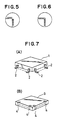
- LSIs shown in FIGS. 7 (a) and (b), respectively, that is, LSI called QFP (Quad Flat Package) and LSI called LCC (Leadless Chip Carrier) or PLCC (Plastic Leadless Chip Carrier) have been recently widely used.
- QFP Quad Flat Package
- LCC Leadless Chip Carrier
- PLCC Plastic Leadless Chip Carrier
- a conductor pattern on a print substrate need be processed into a fluorescent pattern, and in addition, in the case of an electronic part such as the LCC which is not protruded from the package as previously mentioned, it is difficult to perform detection of position, which produces a disadvantage in that a lead terminal cannot be subjected to imaging.
- an arrangement which comprises first light sources and second light sources arranged at positions, respectively, between which is sandwiched an electronic part attracted by an attraction nozzle, a diffusion plate provided between said attraction nozzle and said second light sources, and an imaging means provided below said diffusion plate, wherein the light from said first light sources is irradiated on said electronic part and the transmission light from said electronic part is applied to said imaging means, or the light from said second light sources is irradiated on said electronic part and the reflected light is selectively applied to said imaging means through a through-hole of said diffusion plate to detect a position of said electronic part.
- the light sources are suitably switched according to the state whether or not the terminal pin is protruded from the package body as in electronic parts, particularly LSI, and an image may be obtained by the imaging device.
- Reference numeral 5 designates an attraction nozzle for attracting and transferring an electronic part; 6, a first light source; 7, an upper diffusion plate; 8, a second light source; 9, a lower diffusion plate; 10, an imaging means having a lens 11; and 12, an XY moving head having the attraction nozzle.
- the above-described upper diffusion plate 7 and lower diffusion plate 9 are formed, for example, from frosted glass which generates scattered light at the surface portion, or an indirect illumination member formed of a polyacetal resin which generates scattered light internally.
- QFP Quad Flat Package
- a terminal pin 2 is projected (overflows) from a package body 1
- the QFP is removed out of a stick (not shown) and thereafter the QFP as an electronic part is attracted by the attraction nozzle 5
- the first light sources 6 are turned on as shown in FIG. 1 to irradiate light on the upper diffusion plate 7.
- LCC Longer Chip Carrier
- PLCC Poly Leadless Chip Carrier
- FIG. 3 shows an example which uses an electro-luminescence (merely referred to as EL) in place of the upper diffusion plate and the first light sources in the embodiments shown in FIGS. 1 and 2.
- EL electro-luminescence
- the first light source 6 and the upper diffusion plate 7 are mounted on a support leg 16
- the terminal pin 2 of the QFP is imaged likewise the FIG. 1 embodiment
- the light is irradiated thereon by the first light source 6 through the upper diffusion plate 7 to effect the position detection with the transmission light.
- the image plane caused by the imaging means assumes the state view shown in FIG. 6.
- the QFP, LCC, etc. as the electronic parts are mounted in place on the print substrate (not shown) through the above-described position detection process, and the position detection in a state of being attracted by the attraction nozzle 5 is carried out accurately.
- a computer which stores a normal attracted position reads a deviation between the normal attracted position and a detected position, and the attraction nozzle is displaced through the deviation to mount an electronic part on a print substrate or a table on which a print substrate is disposed is moved through the deviation, after which an electronic part is mounted, then the precision of mounting electronic parts may be enhanced.
- the terminal pins of the leadless type LSI called LCC or PLCC which has many terminal pins and has been considered to be very difficult in detection, may be detected by the reflected light.
- an LC of the QFP type in which a ter minal pin is protruded from a package body may be position-detected by the transmission light.
- position detections of electronic parts of either type of IC in which a terminal pin is protruded from a package body or a type in which a terminal pin is not projected therefrom can be selectively carried out. For this reason, the range of use of the apparatus may be extended. Therefore, the detection operation is easy, which leads to the enhancement of mounting accuracy in the after-mounting process.
- the present is advantageously utilized for a position detector in automatic mounting or automatic insertion of electronic parts.
Landscapes
- Engineering & Computer Science (AREA)
- Manufacturing & Machinery (AREA)
- Microelectronics & Electronic Packaging (AREA)
- Operations Research (AREA)
- Supply And Installment Of Electrical Components (AREA)
- Investigating Materials By The Use Of Optical Means Adapted For Particular Applications (AREA)
Applications Claiming Priority (2)
| Application Number | Priority Date | Filing Date | Title |
|---|---|---|---|
| JP197907/86 | 1986-08-22 | ||
| JP61197907A JPS6354000A (ja) | 1986-08-22 | 1986-08-22 | 電子部品の位置検出装置 |
Publications (3)
| Publication Number | Publication Date |
|---|---|
| EP0257553A2 true EP0257553A2 (fr) | 1988-03-02 |
| EP0257553A3 EP0257553A3 (en) | 1988-10-26 |
| EP0257553B1 EP0257553B1 (fr) | 1993-05-26 |
Family
ID=16382261
Family Applications (1)
| Application Number | Title | Priority Date | Filing Date |
|---|---|---|---|
| EP87112051A Expired - Lifetime EP0257553B1 (fr) | 1986-08-22 | 1987-08-19 | Appareil pour la détection de la position d'un composant électronique |
Country Status (4)
| Country | Link |
|---|---|
| US (1) | US4867569A (fr) |
| EP (1) | EP0257553B1 (fr) |
| JP (1) | JPS6354000A (fr) |
| DE (1) | DE3785978T2 (fr) |
Cited By (6)
| Publication number | Priority date | Publication date | Assignee | Title |
|---|---|---|---|---|
| EP0373373A3 (en) * | 1988-11-14 | 1990-12-12 | Sanyo Electric Co., Ltd. | Electronic parts automatic mounting apparatus |
| EP0460553A3 (en) * | 1990-05-31 | 1992-04-08 | Sanyo Electric Co., Ltd. | Parts mounting apparatus |
| EP0727936A1 (fr) * | 1995-02-20 | 1996-08-21 | Yamaha Hatsudoki Kabushiki Kaisha | Dispositif de reconnaissance d'une pièce |
| US6168003B1 (en) | 1998-05-28 | 2001-01-02 | Siemens Aktiengesellschaft | Method and apparatus for the linear positioning and for the position recognition of a substrate on an onserting unit |
| EP1548396A4 (fr) * | 2002-08-08 | 2011-05-04 | Panasonic Corp | Dispositif d'eclairage, dispositif de reconnaissance comportant ce dispositif d'eclairage et dispositif de montage de piece |
| CN102781212A (zh) * | 2011-05-12 | 2012-11-14 | 雅马哈发动机株式会社 | 吸附状态检查装置、表面安装机和元件试验装置 |
Families Citing this family (24)
| Publication number | Priority date | Publication date | Assignee | Title |
|---|---|---|---|---|
| JPH0244560Y2 (fr) * | 1987-04-03 | 1990-11-27 | ||
| CA1285661C (fr) * | 1988-08-19 | 1991-07-02 | Randy Tsang | Mesurage visuel automatique du placement de dispositifs ensurface d'un substrat |
| JPH03212999A (ja) * | 1990-01-18 | 1991-09-18 | Yamagata Kashio Kk | 電子部品搭載作業装置 |
| US5044072A (en) * | 1990-04-13 | 1991-09-03 | Air-Vac Engineering Company, Inc. | Vision system apparatus and method for component/pad alignment |
| JPH04269607A (ja) * | 1991-02-25 | 1992-09-25 | Mitsui Eng & Shipbuild Co Ltd | 物体の寸法計測装置 |
| US5195234A (en) * | 1991-08-19 | 1993-03-23 | Motorola, Inc. | Method and apparatus for visual alignment of parts |
| JP2586709Y2 (ja) * | 1991-10-07 | 1998-12-09 | 三洋電機株式会社 | 電子部品の位置検出装置 |
| US5304773A (en) * | 1992-02-19 | 1994-04-19 | Trumpf Inc. | Laser work station with optical sensor for calibration of guidance system |
| DE4209524A1 (de) * | 1992-03-24 | 1993-09-30 | Siemens Ag | Verfahren zur Lageerkennung und/oder Teilungsprüfung und/oder Koplanaritätsprüfung der Anschlüsse von Bauelementen und Bestückkopf für die automatische Bestückung von Bauelementen |
| JP3114034B2 (ja) * | 1992-06-05 | 2000-12-04 | ヤマハ発動機株式会社 | 部品実装方法及び部品実装装置 |
| US5214841A (en) * | 1992-09-23 | 1993-06-01 | Emhart Inc. | Machine for placing surface mount components |
| JP3242492B2 (ja) * | 1993-06-14 | 2001-12-25 | ヤマハ発動機株式会社 | 実装機の部品認識装置 |
| US5793121A (en) * | 1994-01-03 | 1998-08-11 | Electro Mechanical Products, Inc. | Low resistance current interrupter |
| JPH08139499A (ja) * | 1994-11-11 | 1996-05-31 | Yamaha Motor Co Ltd | 円筒状部品の認識方法 |
| TW326619B (en) * | 1996-03-15 | 1998-02-11 | Matsushita Electric Industrial Co Ltd | Electronic part mounting apparatus and method thereof |
| US5953812A (en) * | 1997-07-03 | 1999-09-21 | Schlumberger Technologies, Inc. | Misinsert sensing in pick and place tooling |
| JP3678007B2 (ja) * | 1998-07-10 | 2005-08-03 | 松下電器産業株式会社 | 電子部品実装装置における電子部品認識装置および電子部品認識方法 |
| JP4353567B2 (ja) | 1999-01-28 | 2009-10-28 | 富士機械製造株式会社 | 保持装置および撮像方法 |
| DE19921906A1 (de) * | 1999-05-12 | 2000-11-23 | Hella Kg Hueck & Co | Beleuchtungseinrichtung für ein LC-Display |
| US6203082B1 (en) | 1999-07-12 | 2001-03-20 | Rd Automation | Mounting apparatus for electronic parts |
| JP4041768B2 (ja) * | 2002-09-12 | 2008-01-30 | 松下電器産業株式会社 | 部品装着ヘッド |
| JPWO2009096119A1 (ja) * | 2008-01-29 | 2011-05-26 | 株式会社アドバンテスト | 電子部品ハンドリング装置および電子部品の位置検出方法 |
| CN102685288A (zh) * | 2012-04-27 | 2012-09-19 | 昆山威茂电子科技有限公司 | 一种手机产品检验设备 |
| US10620608B2 (en) | 2017-03-07 | 2020-04-14 | Raytheon Company | Collet contrast disk |
Family Cites Families (9)
| Publication number | Priority date | Publication date | Assignee | Title |
|---|---|---|---|---|
| DE1925215A1 (de) * | 1969-05-17 | 1970-11-26 | Philips Patentverwaltung | Anordnung zum selbsttaetigen Kontaktieren der Verbindungsdraehte an Halbleiterdioden |
| DE2643810C2 (de) * | 1976-09-29 | 1983-08-11 | Licentia Patent-Verwaltungs-Gmbh, 6000 Frankfurt | Verfahren zum Einjustieren |
| JPS57103399A (en) * | 1980-12-18 | 1982-06-26 | Matsushita Electric Industrial Co Ltd | Device for mounting and inspecting leadless electronic part |
| US4575637A (en) * | 1983-07-28 | 1986-03-11 | Polaroid Corporation | Part positioning system employing a mask and photodetector array |
| US4628464A (en) * | 1983-10-07 | 1986-12-09 | Westinghouse Electric Corp. | Robotic system for mounting electrical components |
| JPS60103700A (ja) * | 1983-11-11 | 1985-06-07 | 株式会社日立製作所 | 部品の位置決め装置 |
| WO1986004479A1 (fr) * | 1985-01-21 | 1986-07-31 | Fuji Machine Mfg. Co., Ltd. | Procede et appareil de detection de la position d'un outil et appareil electronique de montage d'un outil |
| JPH0797019B2 (ja) * | 1986-06-12 | 1995-10-18 | 松下電器産業株式会社 | 部品認識用照明方法及びその装置 |
| JPH103700A (ja) * | 1996-06-18 | 1998-01-06 | Sony Miyuujitsuku Entertainment:Kk | 金属膜を有する光ディスクの不良化方法 |
-
1986
- 1986-08-22 JP JP61197907A patent/JPS6354000A/ja active Granted
-
1987
- 1987-08-13 US US07/084,962 patent/US4867569A/en not_active Expired - Lifetime
- 1987-08-19 DE DE87112051T patent/DE3785978T2/de not_active Expired - Lifetime
- 1987-08-19 EP EP87112051A patent/EP0257553B1/fr not_active Expired - Lifetime
Cited By (7)
| Publication number | Priority date | Publication date | Assignee | Title |
|---|---|---|---|---|
| EP0373373A3 (en) * | 1988-11-14 | 1990-12-12 | Sanyo Electric Co., Ltd. | Electronic parts automatic mounting apparatus |
| EP0460553A3 (en) * | 1990-05-31 | 1992-04-08 | Sanyo Electric Co., Ltd. | Parts mounting apparatus |
| US5195235A (en) * | 1990-05-31 | 1993-03-23 | Sanyo Electric Co., Ltd. | Parts mounting apparatus |
| EP0727936A1 (fr) * | 1995-02-20 | 1996-08-21 | Yamaha Hatsudoki Kabushiki Kaisha | Dispositif de reconnaissance d'une pièce |
| US6168003B1 (en) | 1998-05-28 | 2001-01-02 | Siemens Aktiengesellschaft | Method and apparatus for the linear positioning and for the position recognition of a substrate on an onserting unit |
| EP1548396A4 (fr) * | 2002-08-08 | 2011-05-04 | Panasonic Corp | Dispositif d'eclairage, dispositif de reconnaissance comportant ce dispositif d'eclairage et dispositif de montage de piece |
| CN102781212A (zh) * | 2011-05-12 | 2012-11-14 | 雅马哈发动机株式会社 | 吸附状态检查装置、表面安装机和元件试验装置 |
Also Published As
| Publication number | Publication date |
|---|---|
| EP0257553B1 (fr) | 1993-05-26 |
| EP0257553A3 (en) | 1988-10-26 |
| DE3785978T2 (de) | 1993-12-02 |
| DE3785978D1 (de) | 1993-07-01 |
| US4867569A (en) | 1989-09-19 |
| JPH0446000B2 (fr) | 1992-07-28 |
| JPS6354000A (ja) | 1988-03-08 |
Similar Documents
| Publication | Publication Date | Title |
|---|---|---|
| EP0257553A2 (fr) | Appareil pour la détection de la position d'un composant électronique | |
| US5502397A (en) | Integrated circuit testing apparatus and method | |
| JPH03104300A (ja) | Ic実装装置及びその方法 | |
| KR19980042368A (ko) | 수평 반송 테스트 핸들러 | |
| KR200372566Y1 (ko) | 인쇄회로기판 표면실장용 지그 | |
| CN118099108A (zh) | 用于集成电路的插座组件的滑动浮动基座 | |
| GB2249672A (en) | Circuit board and apparatus for recognizing the position of a circuit board | |
| KR970007971B1 (ko) | 반도체 집적회로 패키지용 테스트 장치 | |
| EP0496207A3 (en) | Testing device for integrated circuits | |
| CN110024507B (zh) | 作业机 | |
| JPH01152698A (ja) | 電子部品の位置検出装置 | |
| KR950014898A (ko) | 집적 회로 테스팅 장치 | |
| JPH01152699A (ja) | 電子部品の位置検出装置 | |
| KR100312531B1 (ko) | 트레이 피더부가 설치된 표면실장기 | |
| JPH0682227A (ja) | 電子部品の外観検査方法及びその装置 | |
| JPS6234791A (ja) | 視覚装置を有する超精密実装機 | |
| KR20010043895A (ko) | 기판의 1차원적인 위치 지정 및 위치 검출를 위한 방법 및장치 | |
| JPH04219999A (ja) | 部品実装機 | |
| EP3917303B1 (fr) | Machine de montage de composants | |
| JPS62214635A (ja) | 検出装置および検出加工装置 | |
| KR20000016127A (ko) | 반도체 패키지 및 디바이스 소켓_ | |
| JPH0437096A (ja) | 電子部品吸着ノズル | |
| JPH06334329A (ja) | プリント基板 | |
| JPH05275900A (ja) | 部品リードの実装状態検査方法 | |
| KR100189753B1 (ko) | 반도체 패키지의 시험기구 |
Legal Events
| Date | Code | Title | Description |
|---|---|---|---|
| PUAI | Public reference made under article 153(3) epc to a published international application that has entered the european phase |
Free format text: ORIGINAL CODE: 0009012 |
|
| AK | Designated contracting states |
Kind code of ref document: A2 Designated state(s): AT BE CH DE ES FR GB GR IT LI LU NL SE |
|
| RBV | Designated contracting states (corrected) |
Designated state(s): DE FR GB IT SE |
|
| PUAL | Search report despatched |
Free format text: ORIGINAL CODE: 0009013 |
|
| AK | Designated contracting states |
Kind code of ref document: A3 Designated state(s): DE FR GB IT SE |
|
| RHK1 | Main classification (correction) |
Ipc: H05K 13/08 |
|
| 17P | Request for examination filed |
Effective date: 19890426 |
|
| 17Q | First examination report despatched |
Effective date: 19901024 |
|
| GRAA | (expected) grant |
Free format text: ORIGINAL CODE: 0009210 |
|
| AK | Designated contracting states |
Kind code of ref document: B1 Designated state(s): DE FR GB IT SE |
|
| REF | Corresponds to: |
Ref document number: 3785978 Country of ref document: DE Date of ref document: 19930701 |
|
| ET | Fr: translation filed | ||
| ITF | It: translation for a ep patent filed | ||
| PLBE | No opposition filed within time limit |
Free format text: ORIGINAL CODE: 0009261 |
|
| STAA | Information on the status of an ep patent application or granted ep patent |
Free format text: STATUS: NO OPPOSITION FILED WITHIN TIME LIMIT |
|
| 26N | No opposition filed | ||
| EAL | Se: european patent in force in sweden |
Ref document number: 87112051.5 |
|
| PGFP | Annual fee paid to national office [announced via postgrant information from national office to epo] |
Ref country code: SE Payment date: 20010807 Year of fee payment: 15 |
|
| PGFP | Annual fee paid to national office [announced via postgrant information from national office to epo] |
Ref country code: FR Payment date: 20010810 Year of fee payment: 15 |
|
| PGFP | Annual fee paid to national office [announced via postgrant information from national office to epo] |
Ref country code: GB Payment date: 20010815 Year of fee payment: 15 |
|
| REG | Reference to a national code |
Ref country code: GB Ref legal event code: IF02 |
|
| PG25 | Lapsed in a contracting state [announced via postgrant information from national office to epo] |
Ref country code: GB Free format text: LAPSE BECAUSE OF NON-PAYMENT OF DUE FEES Effective date: 20020819 |
|
| PG25 | Lapsed in a contracting state [announced via postgrant information from national office to epo] |
Ref country code: SE Free format text: LAPSE BECAUSE OF NON-PAYMENT OF DUE FEES Effective date: 20020820 |
|
| EUG | Se: european patent has lapsed | ||
| GBPC | Gb: european patent ceased through non-payment of renewal fee |
Effective date: 20020819 |
|
| PG25 | Lapsed in a contracting state [announced via postgrant information from national office to epo] |
Ref country code: FR Free format text: LAPSE BECAUSE OF NON-PAYMENT OF DUE FEES Effective date: 20030430 |
|
| REG | Reference to a national code |
Ref country code: FR Ref legal event code: ST |
|
| PG25 | Lapsed in a contracting state [announced via postgrant information from national office to epo] |
Ref country code: IT Free format text: LAPSE BECAUSE OF NON-PAYMENT OF DUE FEES;WARNING: LAPSES OF ITALIAN PATENTS WITH EFFECTIVE DATE BEFORE 2007 MAY HAVE OCCURRED AT ANY TIME BEFORE 2007. THE CORRECT EFFECTIVE DATE MAY BE DIFFERENT FROM THE ONE RECORDED. Effective date: 20050819 |
|
| PGFP | Annual fee paid to national office [announced via postgrant information from national office to epo] |
Ref country code: DE Payment date: 20060817 Year of fee payment: 20 |