EP0258098A1 - Verkapselte Halbleiteranordnung und Verfahren zu deren Herstellung - Google Patents
Verkapselte Halbleiteranordnung und Verfahren zu deren Herstellung Download PDFInfo
- Publication number
- EP0258098A1 EP0258098A1 EP87401745A EP87401745A EP0258098A1 EP 0258098 A1 EP0258098 A1 EP 0258098A1 EP 87401745 A EP87401745 A EP 87401745A EP 87401745 A EP87401745 A EP 87401745A EP 0258098 A1 EP0258098 A1 EP 0258098A1
- Authority
- EP
- European Patent Office
- Prior art keywords
- stage
- resin package
- semiconductor device
- portions
- semiconductor element
- Prior art date
- Legal status (The legal status is an assumption and is not a legal conclusion. Google has not performed a legal analysis and makes no representation as to the accuracy of the status listed.)
- Granted
Links
Images


Classifications
-
- H—ELECTRICITY
- H10—SEMICONDUCTOR DEVICES; ELECTRIC SOLID-STATE DEVICES NOT OTHERWISE PROVIDED FOR
- H10W—GENERIC PACKAGES, INTERCONNECTIONS, CONNECTORS OR OTHER CONSTRUCTIONAL DETAILS OF DEVICES COVERED BY CLASS H10
- H10W74/00—Encapsulations, e.g. protective coatings
- H10W74/01—Manufacture or treatment
- H10W74/016—Manufacture or treatment using moulds
-
- H—ELECTRICITY
- H10—SEMICONDUCTOR DEVICES; ELECTRIC SOLID-STATE DEVICES NOT OTHERWISE PROVIDED FOR
- H10W—GENERIC PACKAGES, INTERCONNECTIONS, CONNECTORS OR OTHER CONSTRUCTIONAL DETAILS OF DEVICES COVERED BY CLASS H10
- H10W74/00—Encapsulations, e.g. protective coatings
- H10W74/10—Encapsulations, e.g. protective coatings characterised by their shape or disposition
- H10W74/111—Encapsulations, e.g. protective coatings characterised by their shape or disposition the semiconductor body being completely enclosed
- H10W74/121—Encapsulations, e.g. protective coatings characterised by their shape or disposition the semiconductor body being completely enclosed by multiple encapsulations, e.g. by a thin protective coating and a thick encapsulation
-
- H—ELECTRICITY
- H10—SEMICONDUCTOR DEVICES; ELECTRIC SOLID-STATE DEVICES NOT OTHERWISE PROVIDED FOR
- H10W—GENERIC PACKAGES, INTERCONNECTIONS, CONNECTORS OR OTHER CONSTRUCTIONAL DETAILS OF DEVICES COVERED BY CLASS H10
- H10W72/00—Interconnections or connectors in packages
- H10W72/50—Bond wires
- H10W72/541—Dispositions of bond wires
- H10W72/5449—Dispositions of bond wires not being orthogonal to a side surface of the chip, e.g. fan-out arrangements
-
- H—ELECTRICITY
- H10—SEMICONDUCTOR DEVICES; ELECTRIC SOLID-STATE DEVICES NOT OTHERWISE PROVIDED FOR
- H10W—GENERIC PACKAGES, INTERCONNECTIONS, CONNECTORS OR OTHER CONSTRUCTIONAL DETAILS OF DEVICES COVERED BY CLASS H10
- H10W74/00—Encapsulations, e.g. protective coatings
-
- H—ELECTRICITY
- H10—SEMICONDUCTOR DEVICES; ELECTRIC SOLID-STATE DEVICES NOT OTHERWISE PROVIDED FOR
- H10W—GENERIC PACKAGES, INTERCONNECTIONS, CONNECTORS OR OTHER CONSTRUCTIONAL DETAILS OF DEVICES COVERED BY CLASS H10
- H10W90/00—Package configurations
- H10W90/701—Package configurations characterised by the relative positions of pads or connectors relative to package parts
- H10W90/751—Package configurations characterised by the relative positions of pads or connectors relative to package parts of bond wires
- H10W90/756—Package configurations characterised by the relative positions of pads or connectors relative to package parts of bond wires between a chip and a stacked lead frame, conducting package substrate or heat sink
Definitions
- the present invention generally relates to semiconductor devices and methods of producing semiconductor devices, and more particularly to a semiconductor device in which a semiconductor element is sealed by a resin package and a method of producing such a semiconductor device.
- a conventional semiconductor device comprises a stage, a semiconductor element mounted on the stage, a pair of stage bars extending from both sides of the stage for supporting the stage during the production process, leads, wires connecting terminals of the semiconductor element with the corresponding leads, and a generally flat parallelepiped resin package for sealing the semiconductor element and its surrounding parts.
- the pair of stage bars extend up to respective side surfaces of the resin package.
- free tip ends of the stage bars are exposed at the respective side surfaces of the resin package.
- the stage bars are essential to support the stage during the production process, and the excess length of the stage bars are cut along the side surfaces of the resin package only during one of the final production processes.
- the free tip ends of the stage bars are exposed at the side surfaces of the resin package, external moisture can enter the semiconductor device from a gap formed between the resin package and the free tip ends of the stage bars. This moisture will enter inside the semiconductor device along the stage bars and will eventually reach the semiconductor element because the stage bars are connected to the stage which is mounted with the semiconductor element. When the moisture reaches the semiconductor element, the operation characteristic of the semiconductor device becomes deteriorated and causes breakdown of the semiconductor device.
- stage bars are essential in supporting the stage during the production process, there are problems in that the stage bars of the completed semiconductor device lead the external moisture to the semiconductor element and the conventional semiconductor device is insufficiently sealed against moisture.
- stage bars are cut during the production process so that the free tip ends of the stage bars do not extend up to the side surfaces of the resin package.
- a frame-shaped adhesive tape is adhered on the leads and the stage bars before the free tip ends of the stage bars are cut, so as to provide a support for the stage during the remaining production processes.
- an adhesive tape is adhered on each stage bar and the leads adjacent thereto before the free tip ends of the stage bars are cut, so as to provide a support for the stage during the remaining production processes.
- the adhesive tape remains inside the resin package of the completed semiconductor device.
- the moisture is prevented from reaching the semiconductor element directly because the leads are not connected to the stage, but the moisture will advance along a gap formed between the lead and the adhesive tape adhered thereon due to the poor adhesion therebetween.
- the free tip ends of the stage bars exposed at the side surfaces of the resin package are covered by a suitable material so as to prevent the external moisture from entering the semiconductor device from the side surfaces of the resin package where the free tip ends of the stage bars are exposed.
- a suitable material that would satisfactorily adhere on the side surfaces of the resin package and provide a satisfactory seal.
- the material covers only portions of the side surfaces of the resin package where the free tip ends of the stage bars are exposed, the sealing provided thereby against the external moisture is incomplete.
- Another and more specific object of the present invention is to provide a semiconductor device in which free tip ends of stage bars extending from a stage do not extend to side surfaces of a resin package, and the resin package is constituted by an inner resin package portion and an outer resin package portion.
- the free tip ends of the stage bars are located inside the outer resin package portion and are completely sealed.
- the semiconductor device of the present invention the external moisture is positively prevented from reaching a semiconductor element of the semiconductor device.
- the stage bars are completely isolated from leads of the semiconductor device, the external moisture entering from a gap formed between the lead and the outer resin package is positively prevented from reaching the semiconductor element.
- Still another object of the present invention is to provide a method of producing a semiconductor device comprising the steps of providing wires for electrically connecting terminals of a semiconductor element which is mounted on a stage with corresponding leads, forming an inner resin package portion over the semiconductor element and its vicinity including portions of the leads and stage bars which are connected to the stage, cutting free tip ends of the stage bars, and forming an outer resin package portion over the inner resin package portion and the remaining portion of the semiconductor device so that the cut free tip ends of the stage bars are completely sealed inside the outer resin package portion.
- the method of the present invention it is possible to produce the semiconductor device which is sealed against external moisture by simple steps.
- the inner resin package portion a material which would not disturb or damage the wires as the material is injected during the molding of the inner resin package portion, because the materials used for the inner and outer resin package portions need not necessarily be the same.
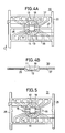
- FIGS.1A and 1B a description will be given on an example of the conventional semiconductor device by referring to FIGS.1A and 1B, so as to facilitate the understanding of the problems of the conventional semiconductor device.
- a conventional semiconductor device comprises a semiconductor element 1 which is mounted on the stage 2, a pair of stage bars 3 and 4 extending from both sides of the stage 2 for supporting the stage 2 during the production process, leads 5, wires 6 connecting terminals of the semiconductor element 1 with the corresponding leads 5, and a generally flat parallelepiped resin package 7 for sealing the semiconductor element 1 and its surrounding parts.
- the pair of stage bars 3 and 4 extend up to respective side surfaces of the resin package 7.
- free tip ends 3a and 4a of the stage bars 3 and 4 are exposed at the respective side surfaces of the resin package 7.
- the stage bars 3 and 4 are essential to support the stage 2 during the production process, and the excess length of the stage bars 3 and 4 is cut along the side surfaces of the resin package 7 only during one of the final production processes.
- the free tip ends 3a and 4a of the stage bars 3 and 4 are exposed at the side surfaces of the resin package 7, external moisture can enter the semiconductor device from a gap formed between the resin package 7 and the free tip ends 3a and 4a of the stage bars 3 and 4.
- This moisture will enter inside the semiconductor device along the stage bars 3 and 4 as respectively indicated by arrows A and B, and will eventually reach the semiconductor element 1 because the stage bars 3 and 4 are connected to the stage 2 which is mounted with the semiconductor element 1.
- the operation characteristic of the semiconductor device becomes deteriorated and causes breakdown of the semiconductor device.
- stage bars 3 and 4 are essential in supporting the stage 2 during the production process, there are problems in that the stage bars 3 and 4 of the completed semiconductor device lead the external moisture to the semiconductor element 1 and the conventional semiconductor device is insufficiently sealed against moisture.
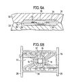
- FIGS.2A through 2C Next, a description will be given on a first embodiment of the semiconductor device according to the present invention by referring to FIGS.2A through 2C.
- a semiconductor device 10 comprises a semiconductor element 11 which is mounted on a stage 12, leads 13, wires 14 connecting terminals of the semiconductor element 11 with the corresponding leads 13, a pair of stage bars 15 and 16 extending from both sides of the stage 12 for supporting the stage 12 during the production process, and a generally flat parallelepiped resin package 17 for sealing the semiconductor device 10.
- the resin package 17 comprises an inner resin package portion 18 and an outer resin package portion 19.
- the inner resin package portion 18 seals the semiconductor element 11 and its surrounding parts including portions of the stage 12, leads 13, the wires 14 and the stage bars 15 and 16.
- the outer resin package portion 19 seals the inner resin package portion 18 and the remaining portions of the semiconductor device 10 not sealed by the inner resin package portion 18.
- the stage bars 15 and 16 do not extend up to respective side surfaces 17a and 17b of the resin package 17. In other words, free tip ends 15a and 16a of the stage bars 15 and 16 end inside the resin package 17. Therefore, the free tip ends 15a and 16a of the stage bars 15 and 16 are completely covered by the resin package 17 and the semiconductor device 10 is satisfactorily sealed against external moisture.
- the external moisture may enter from a gap formed between the resin package 17 and one of the leads 13, but the leads 13 are not connected to the stage 12.
- the moisture entering along the leads 13 may reach the semiconductor element 11 along the wires 14, however, the moisture reaching the semiconductor element 11 along the wires 14 is negligible compared to the moisture reaching the semiconductor element 11 along the stage bars 15 and 16 which are connected to the stage 12. In other words, because the leads 13 are isolated from the stage bars 15 and 16, the moisture entering along the leads 13 will not reach the semiconductor element 11 along the stage bars 15 and 16.
- FIGS.3A, 3B, 3C, 4A, 4B, 5, 6A and 6B those parts which are the same as those corresponding parts in FIGS.2A through 2C are designated by the same reference numerals.
- FIG.3A shows a cross section along a line IIIA-IIIA in FIG.3C
- FIG.3B shows a cross section along a line IIIB-IIIB in FIG.3C
- a lead frame 20 integrally comprises the leads 13 which extend from frames 37 and 38 and a pair of stage bars 26 and 27 which support the stage 12 between frames 28 and 29 which constitute the lead frame 20 together with the frames 37 and 38.
- the semiconductor element 11 is mounted on the stage 12, and the wires 14 are then provided to connect the terminals of the semiconductor element 11 to the corresponding leads 13.
- the lead frame 20 is sandwiched between upper and lower molds 21 and 22 as shown in FIGS.3A and 3B.
- the lower mold 22 has a runner 24 for supplying a first resin which constitutes the inner resin package portion 18 described before.
- the first resin from the runner 24 flows through a passage 39, a flat cavity 23 and a passage 40.
- the air is led out through a hole 40a. It is desirable that the flow of the first resin at the semiconductor element 11 is small so as not to damage the wires 14 and the semiconductor element 11. But on the other hand, it is desirable that the injected first resin properly fills the cavity 23. In the present embodiment, both of these conditions are satisfied because of the rounded shape of the cavity 23 and the passage 39 which supplies the first resin to the cavity 23 and the passage 40 which leads the air out of the molds 21 and 22 through the hole 40a.
- thermosetting resin is used for the first resin, for example.
- FIGS.4A and 4B show a semi-completed semiconductor device 30 which is obtained by the first molding process
- FIG.4B shows the front view viewed in a direction C in FIG.4A with the illustration of the frame 38 and the leads 13 omitted.
- the inner resin package portion 18 seals the semiconductor element 11, the stage 12, the wires 14, base portions of the stage bars 26 and 27 in the vicinity of the stage 12, and portions of the leads 13 in the vicinity of the semiconductor element 11.
- portions of the stage bars 26 and 27 in the vicinity of the frames 28 and 29 are respectively cut off as shown in FIG.5, and a semi-completed semiconductor device 31 is obtained. Even when these portions of the stage bars 26 and 27 are cut off, the stage 12 is still supported satisfactorily by the inner resin package portion 18 which supports the stage 12 via the leads 13 and the remaining stage bars 15 and 16.
- the outer resin package portion 19 is formed by a second molding process.
- the semi-completed semiconductor device 31 is sandwiched between the upper and lower molds 32 and 33 as shown in FIG.6A, and a second resin is injected into a generally flat parallelepiped flat cavity 34 from a runner 35 through a connecting gate portion 36. Then, the unwanted portions of the lead frame 20 and the like are cut off and removed.
- a thermosetting resin is used for the second resin, and as will be described later, the second resin may either be the same as or different from the first resin.
- the cavity 34 is shaped so that the second resin covers the inner resin package portions 18 and the remaining portion of the semi-completed semiconductor device 31 which are not sealed by the inner resin package portion 18.
- the outer resin package portion 19 indicated by a two-dot chain line in FIG.6B is formed when the second resin hardens.
- the inner and outer resin package portions 18 and 19 constitute the resin package 17.
- the same resin in used for the first and second resins it is possible to use an epoxy resin heavily admixed with a filler to 75 to 90 weight percent, where the filler is silica powder having a coefficient of thermal expansion smaller than that of the epoxy resin itself, for example.
- the epoxy resin is heavily admixed with the silica powder, the coefficient of thermal expansion thereof becomes extremely close to the coefficient of thermal expansion of the semiconductor element 11.
- This epoxy resin heavily admixed with the silica powder thus has a characteristic superior to that compared to the conventionally used resin from the point of view of thermal stress, and the sealing effect of the resin package 17 is superior compared to the resin package constituted by the conventional resin due to the high moisture resistance thereof.
- the inner resin package portion 18 can be formed without damaging the wires 14 because the cavity 23 is a small space surrounded by rounded surfaces as described before.
- first and second resins are silicon resin, polyimide resin as a thermosetting resin or polyphenylene sulphide (PPS) resin, liquid crystal polymer (LCP) resin as a thermoplastic resin with a filler such as silica, silicon nitride, or alumina, 0 to 90 weight percent.
- PPS polyphenylene sulphide
- LCP liquid crystal polymer
- thermosetting resin which has a low thermal stress so as to positively prevent undesirable effects on the semiconductor element 11 and its surroundings during the first molding process
- thermosetting resin used for the second resin may have a poor flow rate since the semiconductor element 11, the wires 14 and the like are already sealed and protected by the inner resin package portion 18 when the outer resin package portion 19 is molded during the second molding process, and the selection of the resin which constitutes the resin package (that is, the outer resin package 19) is facilitated.
- a soft material for the first resin by placing emphasis on the prevention of damage to the wires 14 and the semiconductor element 11, and use another material for the second resin by placing emphasis on the moisture resistance.
- the first resin is the thermosplastic resin and the second resin is the thermosetting resin.
- the outer resin is the thermosetting resin, the package itself is heat-resistant in a solder mounting process on a printed circuit board.
- FIGS.7A and 7B those parts which are the same as those corresponding parts in FIGS.2A through 2C are designated by the same reference numerals, and a description thereof will be omitted.
- a semiconductor device 45 shown in FIGS.7A and 7B intermediate portions of the stage bars 26 and 27 are cut off and removed during the production process. As a result, only stage bar portions 41-1 and 42-1 remain connected to the stage 12, and stage bar portions 41-2 and 42-2 remain near the respective side surfaces of the resin package 17. Tip ends 41-1a and 42-1a of the stage bar portions 41-1 and 42-1 are located inside the outer resin package portion 19.
- Outer tip ends 41-2a and 42-2a of the stage bar portions 41-2 and 42-2 are exposed at the side surfaces of the resin package 17, but inner ends 41-2b and 42-2b of the stage bar portions 41-2 and 42-2 are completely isolated from the tip ends 41-1a and 42-1a of the stage bar portions 41-1 and 42-1 by the outer resin package portion 19.
- an inner resin package portion 18A is formed by use of suitable upper and lower molds (not shown) having passages which run along both sides of the stage bars 26 and 27. Otherwise, the production processes are the same as those of the first embodiment of the method described before. According to the present embodiment, the support of the stage 12 is stable when the stage bars 26 and 27 are cut.
Landscapes
- Structures Or Materials For Encapsulating Or Coating Semiconductor Devices Or Solid State Devices (AREA)
- Encapsulation Of And Coatings For Semiconductor Or Solid State Devices (AREA)
- Lead Frames For Integrated Circuits (AREA)
Applications Claiming Priority (2)
| Application Number | Priority Date | Filing Date | Title |
|---|---|---|---|
| JP174854/86 | 1986-07-25 | ||
| JP61174854A JPS6331149A (ja) | 1986-07-25 | 1986-07-25 | 半導体装置 |
Publications (2)
| Publication Number | Publication Date |
|---|---|
| EP0258098A1 true EP0258098A1 (de) | 1988-03-02 |
| EP0258098B1 EP0258098B1 (de) | 1991-04-17 |
Family
ID=15985812
Family Applications (1)
| Application Number | Title | Priority Date | Filing Date |
|---|---|---|---|
| EP87401745A Expired - Lifetime EP0258098B1 (de) | 1986-07-25 | 1987-07-24 | Verkapselte Halbleiteranordnung und Verfahren zu deren Herstellung |
Country Status (5)
| Country | Link |
|---|---|
| US (1) | US4788583A (de) |
| EP (1) | EP0258098B1 (de) |
| JP (1) | JPS6331149A (de) |
| KR (1) | KR910002292B1 (de) |
| DE (1) | DE3769400D1 (de) |
Cited By (11)
| Publication number | Priority date | Publication date | Assignee | Title |
|---|---|---|---|---|
| EP0416573A1 (de) * | 1989-09-05 | 1991-03-13 | Kabushiki Kaisha Toshiba | Harzvergossener Halbleiterbauteil mit Aussenanschlüssen gestaltet für Multifunktionen |
| EP0361194A3 (de) * | 1988-09-30 | 1991-06-12 | Siemens Aktiengesellschaft | Verfahren zum Umhüllen von elektrischen oder elektronischen Bauelementen oder Baugruppen und Umhüllung für elektrische oder elektronische Bauelemente oder Baugruppen |
| EP0478476A1 (de) * | 1990-09-27 | 1992-04-01 | STMicroelectronics S.A. | Gussverfahren für integrierte Schaltungspackungen und Gussform |
| US5358905A (en) * | 1993-04-02 | 1994-10-25 | Texas Instruments Incorporated | Semiconductor device having die pad locking to substantially reduce package cracking |
| WO1996006457A1 (de) * | 1994-08-23 | 1996-02-29 | Dylec Ltd. | Halbleiteranordnung mit wenigstens einem halbleiterbauelement |
| GB2295722A (en) * | 1994-11-30 | 1996-06-05 | Motorola Ltd | Packaging integrated circuits |
| WO1999016132A3 (de) * | 1997-09-22 | 1999-06-17 | Siemens Ag | Verfahren zum herstellen eines kunststoffverbundkörpers sowie kunststoffverbundkörper |
| EP0807971A3 (de) * | 1996-05-14 | 1999-07-28 | Nec Corporation | Elektronische Komponente für Ultrahochfrequenz und Herstellungsverfahren |
| DE102006012615A1 (de) * | 2006-03-20 | 2007-10-11 | Kromberg & Schubert Gmbh & Co. Kg | Umhülltes Bauelement und Verfahren zu dessen Herstellung |
| DE102006047938A1 (de) * | 2006-10-10 | 2008-04-17 | Robert Bosch Gmbh | Gespritztes Kunststoffbauteil mit Einlegeteil |
| WO2010142475A1 (de) * | 2009-06-08 | 2010-12-16 | Robert Bosch Gmbh | Verfahren zur herstellung elektronischer bauteile |
Families Citing this family (45)
| Publication number | Priority date | Publication date | Assignee | Title |
|---|---|---|---|---|
| US4974057A (en) * | 1986-10-31 | 1990-11-27 | Texas Instruments Incorporated | Semiconductor device package with circuit board and resin |
| JP2708191B2 (ja) | 1988-09-20 | 1998-02-04 | 株式会社日立製作所 | 半導体装置 |
| US5208467A (en) * | 1988-07-28 | 1993-05-04 | Semiconductor Energy Laboratory Co., Ltd. | Semiconductor device having a film-covered packaged component |
| JP2522524B2 (ja) * | 1988-08-06 | 1996-08-07 | 株式会社東芝 | 半導体装置の製造方法 |
| US5018003A (en) * | 1988-10-20 | 1991-05-21 | Mitsubishi Denki Kabushiki Kaisha | Lead frame and semiconductor device |
| US4989063A (en) * | 1988-12-09 | 1991-01-29 | The United States Of America As Represented By The Secretary Of The Air Force | Hybrid wafer scale microcircuit integration |
| US5008213A (en) * | 1988-12-09 | 1991-04-16 | The United States Of America As Represented By The Secretary Of The Air Force | Hybrid wafer scale microcircuit integration |
| US5047834A (en) * | 1989-06-20 | 1991-09-10 | International Business Machines Corporation | High strength low stress encapsulation of interconnected semiconductor devices |
| JPH0350758A (ja) * | 1989-07-18 | 1991-03-05 | Toshiba Corp | 樹脂封止型半導体装置 |
| US5349136A (en) * | 1989-08-02 | 1994-09-20 | Matsushita Electric Industrial Co., Ltd. | Mold tool assembly |
| US5030796A (en) * | 1989-08-11 | 1991-07-09 | Rockwell International Corporation | Reverse-engineering resistant encapsulant for microelectric device |
| US5300459A (en) * | 1989-12-28 | 1994-04-05 | Sanken Electric Co., Ltd. | Method for reducing thermal stress in an encapsulated integrated circuit package |
| JP2890662B2 (ja) * | 1990-04-25 | 1999-05-17 | ソニー株式会社 | 樹脂封止型半導体装置の製造方法とそれに用いるリードフレーム |
| US5214846A (en) * | 1991-04-24 | 1993-06-01 | Sony Corporation | Packaging of semiconductor chips |
| US5221812A (en) * | 1991-06-28 | 1993-06-22 | Vlsi Technology, Inc. | System for protecting leads to a semiconductor chip package during testing, burn-in and handling |
| KR930006868A (ko) * | 1991-09-11 | 1993-04-22 | 문정환 | 반도체 패키지 |
| US5197183A (en) * | 1991-11-05 | 1993-03-30 | Lsi Logic Corporation | Modified lead frame for reducing wire wash in transfer molding of IC packages |
| US5331205A (en) * | 1992-02-21 | 1994-07-19 | Motorola, Inc. | Molded plastic package with wire protection |
| US5381599A (en) * | 1993-04-12 | 1995-01-17 | Delco Electronics Corp. | Liquid crystal polymer encapsulated electronic devices and methods of making the same |
| US5430331A (en) * | 1993-06-23 | 1995-07-04 | Vlsi Technology, Inc. | Plastic encapsulated integrated circuit package having an embedded thermal dissipator |
| US5585600A (en) * | 1993-09-02 | 1996-12-17 | International Business Machines Corporation | Encapsulated semiconductor chip module and method of forming the same |
| US5641997A (en) * | 1993-09-14 | 1997-06-24 | Kabushiki Kaisha Toshiba | Plastic-encapsulated semiconductor device |
| US5436203A (en) * | 1994-07-05 | 1995-07-25 | Motorola, Inc. | Shielded liquid encapsulated semiconductor device and method for making the same |
| JPH10116940A (ja) * | 1996-10-09 | 1998-05-06 | Toshiba Corp | 樹脂封止型半導体装置及びその製造方法 |
| US6188897B1 (en) | 1998-08-17 | 2001-02-13 | At&T Wireless Svcs. Inc. | Mobile station roaming in a multiple service provider area |
| US6339253B1 (en) * | 1999-08-30 | 2002-01-15 | Micron Technology, Inc. | Semiconductor package |
| US6576988B2 (en) * | 1999-08-30 | 2003-06-10 | Micron Technology, Inc. | Semiconductor package |
| US6384487B1 (en) | 1999-12-06 | 2002-05-07 | Micron Technology, Inc. | Bow resistant plastic semiconductor package and method of fabrication |
| US6700210B1 (en) | 1999-12-06 | 2004-03-02 | Micron Technology, Inc. | Electronic assemblies containing bow resistant semiconductor packages |
| US6818968B1 (en) * | 2000-10-12 | 2004-11-16 | Altera Corporation | Integrated circuit package and process for forming the same |
| JP4620303B2 (ja) * | 2001-09-20 | 2011-01-26 | 株式会社東海理化電機製作所 | 半導体装置及びその製造方法 |
| JP2003133484A (ja) * | 2001-10-30 | 2003-05-09 | Tokai Rika Co Ltd | 半導体装置及びその製造方法 |
| US6955949B2 (en) * | 2003-10-16 | 2005-10-18 | Kulicke & Soffa Investments, Inc. | System and method for reducing or eliminating semiconductor device wire sweep |
| US7179688B2 (en) * | 2003-10-16 | 2007-02-20 | Kulicke And Soffa Industries, Inc. | Method for reducing or eliminating semiconductor device wire sweep in a multi-tier bonding device and a device produced by the method |
| US6847122B1 (en) | 2003-10-16 | 2005-01-25 | Kulicke & Soffa Investments, Inc. | System and method for preventing and alleviating short circuiting in a semiconductor device |
| CN101040361B (zh) * | 2004-08-17 | 2011-03-30 | 松下电器产业株式会社 | 等离子体显示面板及其制造方法 |
| US7435625B2 (en) * | 2005-10-24 | 2008-10-14 | Freescale Semiconductor, Inc. | Semiconductor device with reduced package cross-talk and loss |
| US7821116B2 (en) * | 2007-02-05 | 2010-10-26 | Fairchild Semiconductor Corporation | Semiconductor die package including leadframe with die attach pad with folded edge |
| CN102104028B (zh) * | 2010-11-05 | 2012-12-12 | 南通富士通微电子股份有限公司 | 半导体塑封体及分层扫描方法 |
| US9069380B2 (en) | 2011-06-10 | 2015-06-30 | Aliphcom | Media device, application, and content management using sensory input |
| US20120313272A1 (en) * | 2011-06-10 | 2012-12-13 | Aliphcom, Inc. | Component protective overmolding |
| US20120313296A1 (en) * | 2011-06-10 | 2012-12-13 | Aliphcom | Component protective overmolding |
| JP5930566B1 (ja) * | 2014-09-29 | 2016-06-08 | 新電元工業株式会社 | 半導体パッケージの製造方法および半導体パッケージ |
| JP6693441B2 (ja) * | 2017-02-27 | 2020-05-13 | オムロン株式会社 | 電子装置およびその製造方法 |
| IT202200024642A1 (it) * | 2022-11-30 | 2024-05-30 | St Microelectronics Srl | Procedimento per produrre dispositivi a semiconduttore e dispositivo a semiconduttore corrispondente |
Citations (2)
| Publication number | Priority date | Publication date | Assignee | Title |
|---|---|---|---|---|
| US3778685A (en) * | 1972-03-27 | 1973-12-11 | Nasa | Integrated circuit package with lead structure and method of preparing the same |
| US3902148A (en) * | 1970-11-27 | 1975-08-26 | Signetics Corp | Semiconductor lead structure and assembly and method for fabricating same |
Family Cites Families (14)
| Publication number | Priority date | Publication date | Assignee | Title |
|---|---|---|---|---|
| JPS5227360A (en) * | 1975-08-27 | 1977-03-01 | Hitachi Ltd | Resin seal-type semiconductor unit |
| NL189379C (nl) * | 1977-05-05 | 1993-03-16 | Richardus Henricus Johannes Fi | Werkwijze voor inkapselen van micro-elektronische elementen. |
| JPS5588358A (en) * | 1978-12-27 | 1980-07-04 | Hitachi Ltd | Resin-sealed semiconductor device |
| JPS5793553A (en) * | 1980-12-03 | 1982-06-10 | Hitachi Ltd | Semiconductor device |
| JPS57100752A (en) * | 1980-12-16 | 1982-06-23 | Toshiba Corp | Semiconductor device |
| JPS57159032A (en) * | 1981-03-27 | 1982-10-01 | Hitachi Ltd | Forming method for package of electronic timepiece |
| JPS58110061A (ja) * | 1981-12-23 | 1983-06-30 | Fujitsu Ltd | 半導体装置等のパッケージ製造方法 |
| JPS58161349A (ja) * | 1982-03-19 | 1983-09-24 | Hitachi Ltd | 半導体装置およびその製造方法 |
| JPS58191457A (ja) * | 1982-05-04 | 1983-11-08 | Toshiba Corp | 半導体装置 |
| JPS58197864A (ja) * | 1982-05-14 | 1983-11-17 | Hitachi Ltd | 半導体装置 |
| JPS59181034A (ja) * | 1983-03-31 | 1984-10-15 | Toshiba Corp | 樹脂封止型半導体装置 |
| JPS6046058A (ja) * | 1983-08-24 | 1985-03-12 | Nec Corp | 半導体装置 |
| JPS60189940A (ja) * | 1984-03-09 | 1985-09-27 | Nec Corp | 樹脂封止型半導体装置の製法 |
| JPS61144853A (ja) * | 1984-12-19 | 1986-07-02 | Hitachi Ltd | リ−ドフレ−ムおよびそれを用いた半導体装置の製造方法 |
-
1986
- 1986-07-25 JP JP61174854A patent/JPS6331149A/ja active Pending
-
1987
- 1987-07-23 KR KR1019870008035A patent/KR910002292B1/ko not_active Expired
- 1987-07-24 US US07/077,292 patent/US4788583A/en not_active Expired - Fee Related
- 1987-07-24 DE DE8787401745T patent/DE3769400D1/de not_active Expired - Lifetime
- 1987-07-24 EP EP87401745A patent/EP0258098B1/de not_active Expired - Lifetime
Patent Citations (2)
| Publication number | Priority date | Publication date | Assignee | Title |
|---|---|---|---|---|
| US3902148A (en) * | 1970-11-27 | 1975-08-26 | Signetics Corp | Semiconductor lead structure and assembly and method for fabricating same |
| US3778685A (en) * | 1972-03-27 | 1973-12-11 | Nasa | Integrated circuit package with lead structure and method of preparing the same |
Non-Patent Citations (4)
| Title |
|---|
| PATENT ABSTRACTS OF JAPAN, vol. 10, no. 32 (E-379)[2089], 7th February 1986; & JP-A-60 189 940 (NIPPON DENKI K.K.) 27-09-1985 * |
| PATENT ABSTRACTS OF JAPAN, vol. 6, no. 185 (E-132)[1063], 21st September 1982; & JP-A-57 100 752 (TOKYO SHIBAURA DENKI K.K.) 23-06-1982 * |
| PATENT ABSTRACTS OF JAPAN, vol. 6, no. 264 (E-150)[1142], 23rd December 1982; & JP-A-57 159 032 (HITACHI SEISAKUSHO K.K.) 01-10-1982 * |
| PATENT ABSTRACTS OF JAPAN, vol. 9, no. 173 (E-329)[1896], 18th July 1985; & JP-A-60 046 058 (NIPPON DENKI K.K.) 12-03-1985 * |
Cited By (15)
| Publication number | Priority date | Publication date | Assignee | Title |
|---|---|---|---|---|
| EP0361194A3 (de) * | 1988-09-30 | 1991-06-12 | Siemens Aktiengesellschaft | Verfahren zum Umhüllen von elektrischen oder elektronischen Bauelementen oder Baugruppen und Umhüllung für elektrische oder elektronische Bauelemente oder Baugruppen |
| EP0416573A1 (de) * | 1989-09-05 | 1991-03-13 | Kabushiki Kaisha Toshiba | Harzvergossener Halbleiterbauteil mit Aussenanschlüssen gestaltet für Multifunktionen |
| US5031024A (en) * | 1989-09-05 | 1991-07-09 | Kabushiki Kaisha Toshiba | Resin sealing type semiconductor device having outer leads designed for multi-functions |
| EP0478476A1 (de) * | 1990-09-27 | 1992-04-01 | STMicroelectronics S.A. | Gussverfahren für integrierte Schaltungspackungen und Gussform |
| FR2667441A1 (fr) * | 1990-09-27 | 1992-04-03 | Sgs Thomson Microelectronics | Procede de moulage pour boitiers de circuit integre et moule. |
| US5358905A (en) * | 1993-04-02 | 1994-10-25 | Texas Instruments Incorporated | Semiconductor device having die pad locking to substantially reduce package cracking |
| WO1996006457A1 (de) * | 1994-08-23 | 1996-02-29 | Dylec Ltd. | Halbleiteranordnung mit wenigstens einem halbleiterbauelement |
| GB2295722A (en) * | 1994-11-30 | 1996-06-05 | Motorola Ltd | Packaging integrated circuits |
| GB2295722B (en) * | 1994-11-30 | 1997-12-17 | Motorola Ltd | Method of packaging integrated circuits |
| EP0807971A3 (de) * | 1996-05-14 | 1999-07-28 | Nec Corporation | Elektronische Komponente für Ultrahochfrequenz und Herstellungsverfahren |
| WO1999016132A3 (de) * | 1997-09-22 | 1999-06-17 | Siemens Ag | Verfahren zum herstellen eines kunststoffverbundkörpers sowie kunststoffverbundkörper |
| DE102006012615A1 (de) * | 2006-03-20 | 2007-10-11 | Kromberg & Schubert Gmbh & Co. Kg | Umhülltes Bauelement und Verfahren zu dessen Herstellung |
| DE102006012615A8 (de) * | 2006-03-20 | 2008-02-28 | Kromberg & Schubert Gmbh & Co. Kg | Umhülltes Bauelement und Verfahren zu dessen Herstellung |
| DE102006047938A1 (de) * | 2006-10-10 | 2008-04-17 | Robert Bosch Gmbh | Gespritztes Kunststoffbauteil mit Einlegeteil |
| WO2010142475A1 (de) * | 2009-06-08 | 2010-12-16 | Robert Bosch Gmbh | Verfahren zur herstellung elektronischer bauteile |
Also Published As
| Publication number | Publication date |
|---|---|
| EP0258098B1 (de) | 1991-04-17 |
| US4788583A (en) | 1988-11-29 |
| DE3769400D1 (de) | 1991-05-23 |
| KR890003009A (ko) | 1989-04-12 |
| KR910002292B1 (ko) | 1991-04-11 |
| JPS6331149A (ja) | 1988-02-09 |
Similar Documents
| Publication | Publication Date | Title |
|---|---|---|
| EP0258098B1 (de) | Verkapselte Halbleiteranordnung und Verfahren zu deren Herstellung | |
| US6410979B2 (en) | Ball-grid-array semiconductor device with protruding terminals | |
| US5750422A (en) | Method for making integrated circuit packaging with reinforced leads | |
| US4837184A (en) | Process of making an electronic device package with peripheral carrier structure of low-cost plastic | |
| KR100225333B1 (ko) | 리이드프레임및반도체장치 | |
| US6818971B2 (en) | Lead frame for resin-molded semiconductor device | |
| KR0141952B1 (ko) | 반도체 패키지 및 그 제조방법 | |
| US6078099A (en) | Lead frame structure for preventing the warping of semiconductor package body | |
| JP3281859B2 (ja) | 混成集積回路装置の製造方法 | |
| EP0430204B1 (de) | Kunststoffumhüllte Halbleiteranordnung | |
| CN217334014U (zh) | 半导体器件 | |
| JPH06132362A (ja) | テープキャリア、それを用いた半導体装置及びその製造方法 | |
| KR100262811B1 (ko) | 에어 캐비티를 가지는 플라스틱 패키지 및 그 제조방법 | |
| JP3367272B2 (ja) | リードフレーム及び半導体装置 | |
| KR940006580B1 (ko) | 접착리드를 이용한 반도체 패키지 구조 및 그 제조방법 | |
| KR100258876B1 (ko) | 반도체 시험용 패키지의 제조방법 | |
| KR200149912Y1 (ko) | 반도체 패키지 | |
| KR200169730Y1 (ko) | 반도체 패키지의 리드프레임 | |
| JPS63273324A (ja) | 樹脂封止型回路装置の製造方法 | |
| KR0134168Y1 (ko) | 반도체 패키지 | |
| JPH02246143A (ja) | リードフレーム | |
| JPH11102924A (ja) | 半導体装置の製造方法 | |
| KR20000014539U (ko) | 반도체 패키지 | |
| KR19990070084A (ko) | 반도체 패키지 및 그 제조방법 | |
| JPH0346358A (ja) | 樹脂封止型半導体装置及びその製造方法 |
Legal Events
| Date | Code | Title | Description |
|---|---|---|---|
| PUAI | Public reference made under article 153(3) epc to a published international application that has entered the european phase |
Free format text: ORIGINAL CODE: 0009012 |
|
| AK | Designated contracting states |
Kind code of ref document: A1 Designated state(s): DE FR GB |
|
| 17P | Request for examination filed |
Effective date: 19880618 |
|
| 17Q | First examination report despatched |
Effective date: 19900328 |
|
| GRAA | (expected) grant |
Free format text: ORIGINAL CODE: 0009210 |
|
| AK | Designated contracting states |
Kind code of ref document: B1 Designated state(s): DE FR GB |
|
| REF | Corresponds to: |
Ref document number: 3769400 Country of ref document: DE Date of ref document: 19910523 |
|
| ET | Fr: translation filed | ||
| PLBE | No opposition filed within time limit |
Free format text: ORIGINAL CODE: 0009261 |
|
| STAA | Information on the status of an ep patent application or granted ep patent |
Free format text: STATUS: NO OPPOSITION FILED WITHIN TIME LIMIT |
|
| 26N | No opposition filed | ||
| PGFP | Annual fee paid to national office [announced via postgrant information from national office to epo] |
Ref country code: GB Payment date: 19930505 Year of fee payment: 7 |
|
| PGFP | Annual fee paid to national office [announced via postgrant information from national office to epo] |
Ref country code: FR Payment date: 19930729 Year of fee payment: 7 |
|
| PGFP | Annual fee paid to national office [announced via postgrant information from national office to epo] |
Ref country code: DE Payment date: 19930917 Year of fee payment: 7 |
|
| PG25 | Lapsed in a contracting state [announced via postgrant information from national office to epo] |
Ref country code: GB Effective date: 19940724 |
|
| GBPC | Gb: european patent ceased through non-payment of renewal fee |
Effective date: 19940724 |
|
| PG25 | Lapsed in a contracting state [announced via postgrant information from national office to epo] |
Ref country code: FR Effective date: 19950331 |
|
| PG25 | Lapsed in a contracting state [announced via postgrant information from national office to epo] |
Ref country code: DE Effective date: 19950401 |
|
| REG | Reference to a national code |
Ref country code: FR Ref legal event code: ST |