EP0259566A2 - Réseaux employés dans des convertisseurs A/N et N/A avec correction des erreurs différentielles - Google Patents
Réseaux employés dans des convertisseurs A/N et N/A avec correction des erreurs différentielles Download PDFInfo
- Publication number
- EP0259566A2 EP0259566A2 EP87110020A EP87110020A EP0259566A2 EP 0259566 A2 EP0259566 A2 EP 0259566A2 EP 87110020 A EP87110020 A EP 87110020A EP 87110020 A EP87110020 A EP 87110020A EP 0259566 A2 EP0259566 A2 EP 0259566A2
- Authority
- EP
- European Patent Office
- Prior art keywords
- output means
- binary
- signals
- analog
- decoding
- Prior art date
- Legal status (The legal status is an assumption and is not a legal conclusion. Google has not performed a legal analysis and makes no representation as to the accuracy of the status listed.)
- Granted
Links
- 239000003990 capacitor Substances 0.000 claims abstract description 41
- 238000010276 construction Methods 0.000 claims abstract description 7
- 230000000750 progressive effect Effects 0.000 claims description 17
- 238000006243 chemical reaction Methods 0.000 claims description 8
- 239000011159 matrix material Substances 0.000 claims 2
- 230000001419 dependent effect Effects 0.000 abstract description 5
- 238000010586 diagram Methods 0.000 description 11
- 230000003213 activating effect Effects 0.000 description 9
- 230000008859 change Effects 0.000 description 4
- 238000004146 energy storage Methods 0.000 description 3
- 230000006872 improvement Effects 0.000 description 3
- 239000007787 solid Substances 0.000 description 3
- 230000004913 activation Effects 0.000 description 2
- 230000006978 adaptation Effects 0.000 description 1
- 230000003247 decreasing effect Effects 0.000 description 1
- 239000003989 dielectric material Substances 0.000 description 1
- 238000007599 discharging Methods 0.000 description 1
- 238000000034 method Methods 0.000 description 1
- 238000004886 process control Methods 0.000 description 1
- 230000009467 reduction Effects 0.000 description 1
- 230000007704 transition Effects 0.000 description 1
Images




Classifications
-
- H—ELECTRICITY
- H03—ELECTRONIC CIRCUITRY
- H03M—CODING; DECODING; CODE CONVERSION IN GENERAL
- H03M1/00—Analogue/digital conversion; Digital/analogue conversion
- H03M1/06—Continuously compensating for, or preventing, undesired influence of physical parameters
- H03M1/0617—Continuously compensating for, or preventing, undesired influence of physical parameters characterised by the use of methods or means not specific to a particular type of detrimental influence
- H03M1/0675—Continuously compensating for, or preventing, undesired influence of physical parameters characterised by the use of methods or means not specific to a particular type of detrimental influence using redundancy
- H03M1/0678—Continuously compensating for, or preventing, undesired influence of physical parameters characterised by the use of methods or means not specific to a particular type of detrimental influence using redundancy using additional components or elements, e.g. dummy components
- H03M1/068—Continuously compensating for, or preventing, undesired influence of physical parameters characterised by the use of methods or means not specific to a particular type of detrimental influence using redundancy using additional components or elements, e.g. dummy components the original and additional components or elements being complementary to each other, e.g. CMOS
-
- H—ELECTRICITY
- H03—ELECTRONIC CIRCUITRY
- H03M—CODING; DECODING; CODE CONVERSION IN GENERAL
- H03M1/00—Analogue/digital conversion; Digital/analogue conversion
- H03M1/66—Digital/analogue converters
- H03M1/74—Simultaneous conversion
- H03M1/76—Simultaneous conversion using switching tree
Definitions
- This invention relates to a digital-to-analog converter. More particularly, the invention relates to a converter which minimizes differential errors. The invention is particularly adapted to correct for differential errors in converters which are monotonic.
- Various types of equipment receive information in analog form.
- Such equipment includes process control equipment, measuring instruments, communications equipment and a wide variety of other equipments.
- Digital computers and data processing systems often receive input parameters in analog form from such equipments and convert these parameters to digital form for processing in the computers or the data processing equipments. After the analog information has been converted to digital information and has been processed, the output information from the digital computers or the data processing equipments is often converted to analog form.
- the user can assimilate the information in ways which would be difficult if the information remained in digital form.
- a good example of the conversions described in the previous paragraph is in the recording and reproduction of music.
- the music is produced in analog form. It is converted to digital form by recently developed data processing techniques and is recorded in digital form on a medium such as a tape or a disc.
- a medium such as a tape or a disc.
- the music is to be reproduced, it is converted again to analog form because this is the form which is necessary to operate sound transducers to give meaning to the listener when he hears the music.
- the converting apparatus now in use also has other problems of long standing.
- the converting apparatus now in use may not be monotonic unless it is quite expensive and complex.
- monotonic is meant that digital information of progressively increasing value is converted to analog information of progressively increasing value without any decrease in the analog value as the digital value progressively increases.
- the converting apparatus now in use also has relatively high differential and integral nonlinearities unless the apparatus is quite complex and expensive. Integral non-linearities result from errors produced in a conversion between digital and analog values over a wide range of such values. Differential nonlinearities result in errors produced in a conversion between digital and analog values over a relatively narrow range of such value.
- the differential errors result primarily from differences in the characteristics of the elements which operate in the converter to provide the output signals. This is particularly true when the output members are formed on an integrated circuit chip. These differences and characteristics result primarily from an inability to produce output elements of substantially uniform characteristics across the chip.
- the differential errors in the converters now in use are specially pronounced for low digital and analog values. The differential errors are more pronounced at low digital values than at high digital values because there are less output elements activated at low rates than at high values and there is accordingly a decreased opportunity to average errors at the low digital values.
- the converting apparatus now in general use also has a problem of major proportions. This results when the converter is operating near the mid-point of its full scale range, or near mid scale, and digital values are increased incrementally by a single digit.
- mid-scale problems result in the 12-bit converters now in use when a binary representation of 2047 is converted to a binary representation of 2048. This results from the fact that the binary representation of 2047 is represented by 011111111111 and a binary representation of 2048 is represented by 100000000000 where the least significant digit is at the right.
- the value of every one of the binary digits changes. As all the binary values change, different weighting elements within the converter are selected. As a result, discontinuities may occur. These discontinuities may prevent the converter from being truly monotonic. This problem even exists in converters which are made quite complex in an attempt to overcome the problem.
- 553,041 is also advantageous in that the number of binary bits capable of being converted on an integrated circuit chip is enhanced and the energy storage members can be easily formed on the chip.
- the use of such energy storage members is also advantageous because they can be formed with relatively small differences between them and because they are relatively stable with changes in temperature.
- This invention provides an improved digital-to-analog converter for eliminating, or at least minimizing, distortions in the conversion between digital and analog values.
- the improvement eliminates, or at least minimizes, differential errors for all digital values
- the invention has particular utility in eliminating distortions, or differential errors, for low digital values.
- the improved converter has particular utility in converting digital signals into audible sound but it can be used in any other application.
- the improved converter has been initially conceived to be operable in a converter of the type disclosed and claimed in application Serial No. 553,041, it will be appreciated that the improvement constituting this invention can be used in any other type of converter.
- a digital-to-analog converter includes a decoding network and a plurality of output members such as capacitors.
- the decoding network receives a plurality of binary signals individually having logic levels respectively coding for binary "1" and binary "0” and individually coding for a binary value of an individual weighted significance and cumulatively coding for an analog value.
- the network decodes the logic levels of the binary signals and activates output members in accordance with such decoding. As the analog value coded by the logic levels of the binary signals increases, the output members previously activated in the plurality remain activated and other output members in the plurality become activated.
- the decoding network and the output members are disposed on an integrated circuit chip.
- the output members Dependent upon their positioning on the chip, the output members have different characteristics which cause errors to be produced in the analog signal, particularly at low analog values. These differences in characteristics of the output members tend to progress linearly with progressive positions across the chip.
- the invention compensates for such errors.
- the invention includes a second converter disposed on the chip with a construction substantially identical to that of the first converter and rotated on the chip substantially 180° relative to the first converter.
- pairs of output members of the same binary significance may have, on the average, a median position in a first direction.
- Individual ones of the output members in the second plurality may have the same positioning, in a second direction co-ordinate with first direction, as corresponding ones of the output members in the first converter.
- Figure 1 illustrates a block diagram of a digital-to-analog converter generally indicated at 11.
- the converter 11 provides on input lines 13 a plurality of binary signals having first and second logic levels which respectively code for binary values of "1" and "0". Each of these signals has an individually weighted binary significance such as 20, 21, 22, etc.
- the converter 11 includes a network 11a which operates upon these signals to convert these signals to a resultant signal on a line 15.
- the signal on the line 15 has an amplitude corresponding to the analog value coded by the logic levels of the signals on the input lines 13.
- the signal on the line 15 is introduced to an operational amplifier 17 across which is connected a storage member such as a capacitor 19.
- the amplifier 17 operates to provide in the capacitor 19 a charge coding for the analog value. This charge is introduced to an output line 23. This charge is periodically discharged when a switch 21 is closed so that a new charge can be developed across the capacitance 19 to represent an updated analog value.
- Figure 2 illustrates the construction of a network (shown schematically in Figure 1 at 11a) which is generally indicated at 10 and which is disclosed and claimed in copending application Serial No. 553,041.
- the network 10 converts into analog form digital values preferably coded by the logic levels of binary signals. These binary signals may have first and second logic levels respectively coding for a binary "1” and a binary "0". Each of the binary signals codes for a binary value of different weighted significance. For example, binary signals are introduced to lines 12, 14 and 16 respectively to code for analog values "1", "2" and "4".
- the network 10 is shown as decoding and converting three (3) binary signals into analog form, the network 10 may be expanded to receive any desired number of binary signals and to convert into analog form the binary values coded by these binary signals.
- the network 10 includes a plurality of double pole switches 30 through 56 (even numbers only).
- the switches 30 and 32 may be considered to constitute a first sub-set; the switches 34, 36, 38 and 40 may be considered to constitute a second sub-set; and the switches 42 through 56 (even numbers only) may be considered to constitute a third sub-set.
- Each sub-set of switches is actuated when a signal having a logic level coding for a binary "1" passes through an individual one of the lines 12, 14 and 16.
- the switches 30 and 32 are actuated in accordance with the logic levels of binary signals produced on the line 12 and coding for the least binary significance; the switches 34, 36, 38 and 40 are actuated in accordance with the logic levels of binary signals produced on the line 14 and coding for an increased binary significance; and the switches 42 through 56 (even numbers only) are actuated in accordance with the logic levels of the binary signals produced on the line 16 and coding for a greater binary significance than those on the lines 12 and 14.
- the signals produced on the lines 12, 14 and 16 are respectively introduced to solenoids S0, S1 and S2 to energize the solenoids when the logic levels of the signals on the lines represent a binary "1".
- the solenoids S0, S1 and S2 actuate the movable poles of the associated switches from the upper positions to the lower positions in Figure 2.
- the association between the solenoids and the switches is represented by broken vertical lines in Figure 2.
- each of the switches 30 through 56 may be replaced by a pair of switches. One of the switches in each pair is closed at each instant and the other switch in the pair is open. The particular switch closed, and the particular switch open, in each pair is dependent upon the logic level of the binary signal controlling the operation of the switches in the pair.
- each of the switches 30 through 56 (even numbers only) may be considered as a pair with the movable contact and one pole defining one switch in the pair and the movable contact and the other pole defining the other switch in the pair.
- One contact of the switch 30 is common with a line 58 and the other contact in the switch 30 is common with a line 60.
- the line 58 may receive a voltage such as -5 volts from a voltage supply.
- one contact in the switch 32 is common with a line 62 and the other contact in the switch is common with the line 60.
- the line 62 may receive an activating voltage such as +5 volts from a voltage supply. Connections are made from the movable poles of the switch 30 to first contacts of the switches 34 and 36. Similarly, connections are made from the movable poles of the switch 32 to first contacts of the switches 38 and 40.
- the second contact of the switch 34 is connected to the line 58 and the second contact of the switch 36 is connected to the line 62. Connections are correspondingly made from the second contact of the switch 38 to the line 58 and from the second contact of the switch 40 to the line 62.
- the movable poles of the switches 34, 36, 38 and 40 are respectively connected to first contacts of the switches 42 and 44, first contacts of the switches 46 and 48, first contacts of the switches 50 and 52 and first contacts of the switches 54 and 56.
- the second contacts of the switches 42, 46, 50 and 54 are connected to the line 58 and the second contacts of the switches 44, 48, 52 and 56 are connected to the line 62.
- the movable poles of the switches 44 through 56 are connected to first terminals of storage members such as capacitors 66 through 80 (even numbers only).
- the capacitors 66 through 80 are respectively designated by the numeral "H” through "A”.
- the second terminals of the capacitors 66 through 80 are connected to a line 82.
- the network 10 shown in Figure 2 and described above may be considered to be recursive.
- the switches in each sub-set have the same connections to the switches in the sub-sets of next highest and lowest significance as the switches in other sub-sets have to the switches of next highest and lowest significance relative to such other sub-sets.
- This recursive relationship allows the network 10 to be expanded easily to respond to the logic levels of any desired number of input signals each of which has an individual binary significance.
- the movable poles of the switches 30 through 56 are shown in Figure 2 in the positions in which they are operative when the binary signals introduced to the switches have a logic level of "0". With the movable contacts of the switches 30 through 56 (even numbers only) in the positions shown in Figure 2, no connections are established between any of the capacitors 66 through 80 (even numbers only) and the activating line 62. As a result, none of the capacitors 66 through 80 (even numbers only) is charged by the voltage on the line 62. This corresponds to an analog value of "0" in accordance with the logic levels of the binary signals introduced to the lines 12, 14 and 16.
- a connection is established which includes the interpolation line 60, the switch 32, the switch 40, the switch 56 and the capacitance 80.
- This causes the capacitance 80 to become charged to a level dependent upon the voltage on the interpolation line 60.
- This voltage may be a constant or reference such as ground or it may be variable in accordance with the disclosure in application Serial No. 755,170 filed by me on July 15, 1985, for "Apparatus for Converting Between Digital and Analog Values" and assigned of record to the assignee of record of this application.
- the signal on the line 60 may be variable to indicate the analog value of binary signals of lower binary significance than the signals on the line 12, 14 and 16.
- the charge in the capacitance 80 is introduced to the line 82 to provide an indication of the analog value of "1".
- the capacitance 80 is then discharged through a switch (corresponding to the switch 21 in Figure 1), which is periodically closed to the ground.
- the charging and discharging cycle of the capacitances 66 through 80 (even numbers only) is fully disclosed in co-pending application Serial No. 755,170 filed by me on July 15, 1985, and assigned of record to the assignee of record of this application.
- a connection is established which includes the interpolating line 60, the switch 30, the switch 36, the switch 48 and the capacitance 72.
- the capacitance 72 accordingly becomes charged to a value dependent upon the voltage on the interpolating line 60.
- the capacitance 80 becomes charged through a circuit including the line 62, the switch 40 and the switch 56.
- the capacitance 72 becomes charged through a circuit including the line 62, the switch 36 and the switch 48.
- the charges in the capacitances 72 and 80 are introduced to the line 82 to indicate an analog value of "2".
- the capacitance 76 becomes simultaneously charged through a circuit including the interpolating line 60, the switch 32, the switch 38 and the switch 52.
- the voltage on the interpolating line 60 may have an analog value coding for the value of binary bits of lower binary significance than the lines 12, 14 and 16.
- the voltage may be produced on the interpolating line 60 by a converter such as shown in Figure 2 or by a conventional converter.
- the output voltage on the line 82 connected to all of the capacitors 66 through 80 may represent only three binary bits if the interpolating line 60 is grounded or may represent an increased number of binary bits if the interpolating line 58 receives the voltage produced in a converter of lower binary significance than that shown in Figure 2.
- Figure 4 indicates the capacitances which are respectfully connected to the lines 62 and 60 for each analog value coded by logic levels of the binary signals on the lines 12, 14 and 16.
- the logic levels of the binary signals introduced to the lines 12, 14 and 16 are indicated in the first three columns in that figure. The analog significance of these binary signals is shown at the top of each of these columns.
- the remaining columns indicates the state of operation of the capacitances 66 through 80 (even numbers only).
- These capacitances are respectively indicated in Figure 4 by the letters "H” through "A” to correspond to the letters indicated for these capacitances in Figure 2.
- the last column in Figure 4 indicated the particular one of the capacitances to be connected to the interpolation line 60 for each analog value coded by the logic levels of the binary signals on the lines 12, 14 and 16.
- two diagonal lines 90 and 92 are provided.
- the capacitances indicated to the left of the line 90 represent those connected to the activation line 62 for the different analog values.
- the capacitances isolated between the lines 90 and 92 are those which are connected to the interpolation line 60 for each analog value. These capacitances correspond to those indicated in the last column in Figure 4.
- the capacitance connected to the interpolation line 60 for each analog value is the one to be connected next to the activation line 62 when the analog value represented by the logic levels of the binary signals coded on the lines 12, 14 and 16 increases.
- the capacitances shown to the right of the line 92 in Figure 4 are connected to the line 58 for the different analog values.
- Figure 5 indicates the disposition on an integrated circuit chip, generally indicated at 94, of the circuitry shown in Figure 1.
- the capacitances "A” through “H” are displaced at progressive positions in a y-direction (vertical direction) on a chip.
- the relative positions of the capacitances "A” through “H” in the y-direction on the chip 94 are also illustrated in Figure 3a.
- Figure 3a also indicates the relative analog value in which each of the capacitances "A” through “H” is connected to the activating line 62.
- Figure 3b illustrates the relative disposition of the capacitors "A” through “H” in the y-direction and also indicates in the x-direction the analog value in which each of such capacitances becomes connected to the activating line 62.
- the relative positions of the capacitances "A” through “H” are indicated in Figure 3b by hollow triangles.
- Figure 3b also illustrates by hollow rectangles the average position of the activated capacitances for each analog value. For example, for an analog value of "2", the average position of the activated capacitances in the y-direction is at "5" since the capacitance "A" is at a position of "1” and the capacitance "E” is at a position of "9". As will be seen, the average position of the activated capacitances in the y-direction varies between “1” and “8” for different analog values between “1” and "8".
- FIG. 3a Each of the capacitances shown in Figure 3a should have equal value.
- Figure 3c illustrates how the capacitances vary in value between the capacitance "A” (represented as “C A ”) at the lowest position in the y-direction and the capacitance "H” (represented as “C H ”) at the highest position in the y-direction.
- the values of the capacitances tend to vary linearly with progressive positions in the y-direction. This results from processing variations such as gradients in the thickness of the oxide dielectrics in the capacitors. These gradients may be in the range of one percent (1%) to two percent (2%) over a distance of 200 mils.
- the difference between a unit capacitor value in the transition from an analog value of "4" to an analog value of "5" may be in the order of one percent (1%) since the distances between the capacitances "G" and "B" may be in the order of 100 mils.
- Figure 3d indicates the changes in the differential linearity of the capacitors "A" through “H” from a median value for each of the analog values between “1" and "8". As will be seen, the differential non-linearities change value from one side of the median value to the other for each progressive analog value.
- Figure 3d illustrates the changes in relation to the value of the capacitance to be connected next to the interpolating line 60 for each progressive analog value. As will be seen, there are relatively great swings in the values of the capacitances to be connected next to the interpolating line 60 for each progressive analog value. These changes in the values of the capacitance connected to the interpolating line 60 for each analog value are then introduced into the activating line 62 for the next analog value of increasing magnitude.
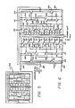
- Figure 6 illustrates a circuit diagram constituting one embodiment of the invention.
- the circuit diagram shown in Figure 2 and described above is shown at the left end and a duplicate circuit is shown at the right end.
- the circuit at the right end is inverted, or rotated 180°, relative to the circuit at the left end.
- the components at the right end of Figure 6 are provided with the same designations as the corresponding components at the left end of Figure 6 except for the addition of a numeral "1" before such numbers.
- a capacitance at the left end of Figure 6 is designated as "66” and the corresponding capacitance at the right end of Figure 6 is designated as "166".
- Both circuits have the line 82 connected to the capacitances in the circuits.
- Figure 7a is a chart similar to the chart of Figure 3a. However, Figure 7a shows the relative positioning of the capacitors "A" through “H” (66 through 80, even numbers only) and the capacitors A ⁇ through H ⁇ (166 through 180, even numbers only) in the Y-direction on the integrated circuit chip 94 in Figure 5. As will be seen, the positions of the capacitances A ⁇ through H ⁇ are inverted relative to the positions of the corresponding ones of the capacitors "A" through “H”. In Figure 7, the capacitors A ⁇ through H ⁇ respectively correspond to the capacitors A through H.
- Figure 7b indicates by hollow triangles the relative positions of the capacitances "A” through “H” and the capacitances "A ⁇ ” through “H ⁇ ” in the y-direction on the integrated circuit chip 94 for analog values from 1 through 8.
- the analog values are specified along the horizontal coordinate in Figure 7b and the positions of the different capacitances in the y-direction on the chip 94 are indicated along the vertical coordinate in Figure 7b.
- the median position of the capacitances for each analog value from 1 through 8 is represented in Figure 7b by hollow rectangles. As will be seen in Figure 7b, the median position for activated capacitances for each analog value from 1 through 8 remains constant.
- Figure 7c indicates the changes in the values of the capacitances "A” through “H” as a result of the differences in their positioning in the y-direction on the chip 94 and also indicates the changes in the values of the capacitances "A ⁇ " through “H ⁇ ” as a result of the differences in their positioning on the chip.
- Figure 7d indicates that there are no changes in the differential linearity of the capacitances connected to the interpolating line 60 for the different analog values from 1 through 8.
- the capacitances In addition to linear gradients in the value of the capacitances 66 through 80 (even numbers only) and the capacitances 166 through 180 (even numbers only) in accordance with the positioning of the capacitances on the integrated circuit chip, the capacitances also have lithographic variations in individual ones of such capacitances. These variations tend to occur on a somewhat random basis on the integrated circuit chip 94. These variations may occur in the range of one tenth of one percent (0.1%) to two tenths of one percent (0.2%). These variations are reduced by the square root of two ( 2) in the converter shown in Figure 6 and described above. This reduction occurs because there are twice as many capacitances on the chip 94 for the embodiment shown in Figure 6 as for the embodiment shown in Figure 7.
- the converter shown in Figure 6 and described above has other important advantages over the converters of the prior art. For example, since differential errors have been eliminated, or at least minimized, the converters can be used to convert digital signals to sound with complete fidelity over the full range of amplitudes. This is particularly important at low amplitudes because the converters of the prior art have introduced distortions into the sound at low amplitudes.
- output members may be transistors such as disclosed and claimed in application Serial No. 383,544.
- the output members may be also resistors such as ion-implanted resistors.
- Figure 8 illustrates a network which is generally indicated at 200 and which is known in the prior art for converting digital values, such as binary coded values, to analog values.
- the network includes a plurality of single-pole single-throw switches, 201, 202, 203, 204, 205, 206, 207, 208, 209, 209, 210, 211, 212, 213 and 214.
- the switches 201 and 202 may be considered as the switches of a first subset which is responsive to a binary signal on a first line 216.
- the signal on the line 216 causes a solenoid 218 to be energized when the signal has a logic level coding for a binary value of "1".
- the solenoid 218 When the solenoid 218 is energized, it causes the switch 202 to become closed and the switch 201 to become opened.
- the switches 201 and 202 are biased to positions providing a closure of the switch 201 and an opening of the switch 202 when a signal having a logic level coding for a binary value of "0" is produced on the line 216.
- mechanical switches are shown in Figure 8, it will be appreciated that other types of converters such as transistors may also be used without departing from the scope of the invention.
- the switches 203, 204, 205 and 206 are included in a second subset which is responsive to the logic level of the signal on a line 220.
- a solenoid 222 becomes energized and causes the switches 204 and 206 to become closed and the switches 203 and 205 to become opened.
- the switches 204 and 206 become opened, and the switches 205 and 207 become closed, when a signal having a logic level coding for a binary value of "0" is produced on the line 220.
- the switches 208, 210, 212 and 214 become closed, and the switches 207, 209, 211 and 213 become opened, when a signal having a logic level coding for a binary "1" is produced on a line 224 to energize a solenoid 226.
- the switches 208, 210, 212 and 214 become opened, and the switches 207, 209, 211 and 213 become opened, when a signal having a logic level coding for a binary "0" is produced on the line 224.
- a resistance ladder formed by resistors 230, 232, 234, 236, 238, 240, 242 and 244 is connected in series between an energizing potential 248 and a reference potential such as ground.
- the resistors 230 through 244 (even numbers only) are connected to first terminals of the switches 207, 208, 209, 210, 211, 212, 213 and 214. Connections are made from second terminals of the switches 207 and 208 to a first terminal of the switch 204, from second terminals 209 and 210 to a first terminal of the switch 203, from second terminals of the switches 211 and 212 to a first terminal of the switch 206 and from second terminals of switches 213 and 214 to a first terminal of the switch 205.
- the second terminals of the switches 203 and 204 and of the switches 205 and 206 respectively are common with first terminals of the switches 202 and 211.
- the second terminals of the switches 201 and 202 are connected to an output line 250.
- the embodiment shown in Figure 8 produces a voltage on the output line 250 to code on an analog basis for the logic levels of the binary signals on the lines 216, 220 and 224. For example, for a logic level of "1" on the line 220, the switches 204 and 206 become closed and the switches 203 and 205 become opened. Under such circumstances, when the potential on the terminal 248 is +10 volts, a potential of 2 volts is produced on the input line 250 to represent an analog value of "2".
- the resistances 230 through 244 (even numbers only) would have equal values.
- the values of the resistances 230 through 244 vary progressively on an integrated circuit chip such as in a linear relationship.
- the resistances 230 through 244 may illustratively have progressive values between 1000 ohms and 1007 ohms.
- Column 3 in Figure 9 illustrates the proportionate resistance value of each resistance in the resistance network (when added to the resistances above it in the resistance network in Figure 8) in comparison to the total value of all of the resistances in the resistance network.
- Figure 10 illustrates the network 200 when included in an embodiment of this invention with a duplicate network generally indicated at 200a.
- the network 200a is inverted relative to the network 200 and is disposed in back-to-back relationship to the network 200.
- resistances 244a, 242a, 240a, 238a, 236a, 234a, 232a and 230a in the network 200a are respectively paired with the resistances 230, 232, 234, 236, 238, 240, 242, and 244 in the network 200.
- the first two columns of Figure 11 are identical to the first two columns of Figure 9.
- the third column indicates the paired resistance in the network 200a corresponding to the particular resistance indicated in the first column of Figure 11.
- the fourth column in Figure 11 indicates the values of the resistances shown in the third column of Figure 11.
- each pair of resistances in the embodiment of Figure 10 is connected in parallel.
- the fifth column in Figure 11 indicates the value of each such parallel pair of resistances.
- the sixth column in Figure 11 indicates the value determined by using the value in the sixth column of Figure 11 as a numerator (when added with all of the values above it in the sixth column of Figure 11) and the sum of all of the resistance values in the sixth column of Figure 11 as a denominator.
- the seventh column indicates the ideal values corresponding to those specified in the fourth column of Figure 9. These represent ideal conditions where all of the resistances in the resistance ladder have values of one thousand (1000) ohms.
- the values in the seventh column of Figure 11 represent the value of each ideal resistance (when added to the values of all of the ideal resistances above it in the seventh column of Figure 11) as a numerator and the sum of all of these ideal resistances as a denominator.
- the eighth column in Figure 11 indicates the difference between the paired values in the sixth and seventh columns of Figure 11, this difference then being multiplied by one hundred (100).
- the value in the eighth column of Figure 8 accordingly represents the percentage deviation or error from an optimum value in the output indications of the network shown in Figure 10.
- the maximum deviation or error is one ten thousandth of one percent (0.0001%). This compares to a maximum error of one tenth of one percent (0.1%) for the prior art embodiment shown in Figure 8.
- the embodiment shown in Figure 10 provides output indications one thousand times more accurate that the prior art embodiment shown in Figure 8.
- the invention can be used with any converter.
- the invention can be used with any types of decoders which are of the thermometer type - that is, decoders in which, for progressively increasing analog values, output members (such as capacitances) previously activated remain activated and additional output members such as capacitances become activated. This is represented by the embodiment shown in Figures 5 and 6.
- the invention can also be used with decoders which are not of the thermometer type.
- An example of this type of converter is the binary-weighted tree decoder shown in Figure 8 and 10.
Landscapes
- Engineering & Computer Science (AREA)
- Theoretical Computer Science (AREA)
- Analogue/Digital Conversion (AREA)
Applications Claiming Priority (2)
| Application Number | Priority Date | Filing Date | Title |
|---|---|---|---|
| US884472 | 1986-07-11 | ||
| US07/884,472 US4875046A (en) | 1986-07-11 | 1986-07-11 | Centroiding algorithm for networks used in A/D and D/A converters |
Publications (3)
| Publication Number | Publication Date |
|---|---|
| EP0259566A2 true EP0259566A2 (fr) | 1988-03-16 |
| EP0259566A3 EP0259566A3 (en) | 1990-07-11 |
| EP0259566B1 EP0259566B1 (fr) | 1994-06-01 |
Family
ID=25384694
Family Applications (1)
| Application Number | Title | Priority Date | Filing Date |
|---|---|---|---|
| EP87110020A Expired - Lifetime EP0259566B1 (fr) | 1986-07-11 | 1987-07-10 | Réseaux employés dans des convertisseurs A/N et N/A avec correction des erreurs différentielles |
Country Status (5)
| Country | Link |
|---|---|
| US (1) | US4875046A (fr) |
| EP (1) | EP0259566B1 (fr) |
| JP (1) | JP2583514B2 (fr) |
| CA (1) | CA1284384C (fr) |
| DE (1) | DE3789927T2 (fr) |
Cited By (1)
| Publication number | Priority date | Publication date | Assignee | Title |
|---|---|---|---|---|
| EP0545295A3 (fr) * | 1991-12-02 | 1995-07-12 | Hughes Aircraft Co |
Families Citing this family (32)
| Publication number | Priority date | Publication date | Assignee | Title |
|---|---|---|---|---|
| JP2597712B2 (ja) * | 1989-05-22 | 1997-04-09 | 株式会社東芝 | ディジタル・アナログ変換器 |
| JP2605874B2 (ja) * | 1989-06-29 | 1997-04-30 | 日本電気株式会社 | D―a変換器 |
| JPH04329025A (ja) * | 1991-04-30 | 1992-11-17 | Toshiba Corp | D/aコンバータ |
| JP3000499B2 (ja) * | 1992-08-25 | 2000-01-17 | セイコーインスツルメンツ株式会社 | Da変換回路 |
| US5534863A (en) * | 1994-01-06 | 1996-07-09 | Level One Communications, Inc. | Low resolution, high linearity digital-to-analog converter without trim |
| US7064376B2 (en) * | 1996-05-24 | 2006-06-20 | Jeng-Jye Shau | High performance embedded semiconductor memory devices with multiple dimension first-level bit-lines |
| US5748547A (en) * | 1996-05-24 | 1998-05-05 | Shau; Jeng-Jye | High performance semiconductor memory devices having multiple dimension bit lines |
| US20050036363A1 (en) * | 1996-05-24 | 2005-02-17 | Jeng-Jye Shau | High performance embedded semiconductor memory devices with multiple dimension first-level bit-lines |
| GB2368209B (en) * | 1998-01-08 | 2002-06-12 | Fujitsu Ltd | Cell array circuitry |
| US6100834A (en) * | 1998-05-15 | 2000-08-08 | Pairgain Technologies, Inc. | Recursive multi-bit ADC with predictor |
| US6016019A (en) * | 1998-05-28 | 2000-01-18 | Microchip Technology Incorporated | Capacitor array arrangement for improving capacitor array matching |
| US6130635A (en) * | 1998-08-03 | 2000-10-10 | Motorola Inc. | Method of converting an analog signal in an A/D converter utilizing RDAC precharging |
| DE60013245T2 (de) * | 1999-01-22 | 2005-01-13 | Multigig Ltd., Wilby Wellingborough | Elektronische schaltungsanordnung |
| US7764130B2 (en) * | 1999-01-22 | 2010-07-27 | Multigig Inc. | Electronic circuitry |
| AU2001234551A1 (en) * | 2000-01-28 | 2001-08-07 | Semtech New York Corporation | Pointing device with z-axis functionality and reduced component count |
| US6512471B2 (en) | 2000-01-28 | 2003-01-28 | Semtech Corporation | Intentionally non-monotonic digital-to-analog converter |
| ATE400923T1 (de) * | 2000-05-11 | 2008-07-15 | Multigig Ltd | Elektronischer pulserzeuger und oszillator |
| US6693468B2 (en) | 2001-06-12 | 2004-02-17 | Rf Micro Devices, Inc. | Fractional-N synthesizer with improved noise performance |
| US6779010B2 (en) | 2001-06-12 | 2004-08-17 | Rf Micro Devices, Inc. | Accumulator with programmable full-scale range |
| US7003049B2 (en) * | 2001-06-12 | 2006-02-21 | Rf Micro Devices, Inc. | Fractional-N digital modulation with analog IQ interface |
| US6448831B1 (en) | 2001-06-12 | 2002-09-10 | Rf Micro Devices, Inc. | True single-phase flip-flop |
| US6710664B2 (en) * | 2002-04-22 | 2004-03-23 | Rf Micro Devices, Inc. | Coarse tuning for fractional-N synthesizers |
| US7064591B1 (en) | 2004-05-11 | 2006-06-20 | Rf Micro Devices, Inc. | Coarse tuning for fractional-N synthesizers |
| US7023282B1 (en) | 2004-05-11 | 2006-04-04 | Rf Micro Devices, Inc. | Coarse tuning for fractional-N synthesizers having reduced period comparison error |
| US7209065B2 (en) * | 2004-07-27 | 2007-04-24 | Multigig, Inc. | Rotary flash ADC |
| WO2007120361A2 (fr) * | 2005-12-27 | 2007-10-25 | Multigig Inc. | Système et procédé de conversion analogique-numérique flash à horloge rotative |
| WO2008121857A1 (fr) | 2007-03-29 | 2008-10-09 | Multigig Inc. | Système et procédé d'inversion d'onde pour un oscillateur rotatif à onde progressive |
| US10312922B2 (en) | 2016-10-07 | 2019-06-04 | Analog Devices, Inc. | Apparatus and methods for rotary traveling wave oscillators |
| US10277233B2 (en) | 2016-10-07 | 2019-04-30 | Analog Devices, Inc. | Apparatus and methods for frequency tuning of rotary traveling wave oscillators |
| US11527992B2 (en) | 2019-09-19 | 2022-12-13 | Analog Devices International Unlimited Company | Rotary traveling wave oscillators with distributed stubs |
| US11264949B2 (en) | 2020-06-10 | 2022-03-01 | Analog Devices International Unlimited Company | Apparatus and methods for rotary traveling wave oscillators |
| US11539353B2 (en) | 2021-02-02 | 2022-12-27 | Analog Devices International Unlimited Company | RTWO-based frequency multiplier |
Family Cites Families (9)
| Publication number | Priority date | Publication date | Assignee | Title |
|---|---|---|---|---|
| US4198622A (en) * | 1978-02-21 | 1980-04-15 | National Semiconductor Corporation | Double digital-to-analog converter |
| JPS57133721A (en) * | 1981-02-13 | 1982-08-18 | Sony Corp | Da converting circuit |
| CA1250051A (fr) * | 1983-11-18 | 1989-02-14 | Brooktree Corporation | Appareil de conversion de donnees numeriques en donnees analogiques |
| US4543560A (en) * | 1984-02-17 | 1985-09-24 | Analog Devices, Incorporated | Two-stage high resolution digital-to-analog converter |
| US4658240A (en) * | 1984-05-07 | 1987-04-14 | Brooktree Corporation | Apparatus for converting data between analog and digital values |
| JPS6126330A (ja) * | 1984-07-16 | 1986-02-05 | Toshiba Corp | 抵抗分圧回路 |
| JPH071870B2 (ja) * | 1984-07-31 | 1995-01-11 | 日本電気株式会社 | ディジタル/アナログ変換回路 |
| JPS61240716A (ja) * | 1985-04-17 | 1986-10-27 | Mitsubishi Electric Corp | ディジタルアナログコンバ−タ |
| US4665380A (en) * | 1985-07-15 | 1987-05-12 | Brooktree Corporation | Apparatus for converting between digital and analog values |
-
1986
- 1986-07-11 US US07/884,472 patent/US4875046A/en not_active Expired - Lifetime
-
1987
- 1987-05-28 CA CA000538297A patent/CA1284384C/fr not_active Expired - Lifetime
- 1987-07-09 JP JP62169915A patent/JP2583514B2/ja not_active Expired - Lifetime
- 1987-07-10 EP EP87110020A patent/EP0259566B1/fr not_active Expired - Lifetime
- 1987-07-10 DE DE3789927T patent/DE3789927T2/de not_active Expired - Lifetime
Cited By (1)
| Publication number | Priority date | Publication date | Assignee | Title |
|---|---|---|---|---|
| EP0545295A3 (fr) * | 1991-12-02 | 1995-07-12 | Hughes Aircraft Co |
Also Published As
| Publication number | Publication date |
|---|---|
| EP0259566B1 (fr) | 1994-06-01 |
| DE3789927T2 (de) | 1994-09-08 |
| US4875046A (en) | 1989-10-17 |
| JP2583514B2 (ja) | 1997-02-19 |
| JPS6330024A (ja) | 1988-02-08 |
| EP0259566A3 (en) | 1990-07-11 |
| DE3789927D1 (de) | 1994-07-07 |
| CA1284384C (fr) | 1991-05-21 |
Similar Documents
| Publication | Publication Date | Title |
|---|---|---|
| EP0259566B1 (fr) | Réseaux employés dans des convertisseurs A/N et N/A avec correction des erreurs différentielles | |
| US5243347A (en) | Monotonic current/resistor digital-to-analog converter and method of operation | |
| EP0102609B1 (fr) | Convertisseur numérique-analogique | |
| US5495245A (en) | Digital-to-analog converter with segmented resistor string | |
| US5283580A (en) | Current/resistor digital-to-analog converter having enhanced integral linearity and method of operation | |
| US11133818B2 (en) | Interpolation digital-to-analog converter (DAC) | |
| JPH07193509A (ja) | サーモメータ・バイナリ・エンコード方法 | |
| JP2004519964A (ja) | D/a変換器 | |
| JPH05500742A (ja) | 2↑(↑n↑−↑1↑)個の比較器を用いた並列アナログデジタル変換器換器 | |
| EP1741190B1 (fr) | Procede destine a ameliorer la reduction d'erreurs dans un convertisseur numerique-analogique et convertisseur numerique-analogique dans lequel ce procede est applique | |
| US5640162A (en) | Digital-to-analog converter with binary coded inputs to produce a plurality of outputs in the form of thermometer code | |
| EP0209835B1 (fr) | Appareil de conversion de valeurs numériques en valeurs analogiques | |
| CN111801894B (zh) | 数模转换器系统 | |
| US6452527B2 (en) | Current adding type D/A converter | |
| JPH04162830A (ja) | D/aコンバータ | |
| EP0241733B1 (fr) | Convertisseur analogique-numérique rapide à haute résolution | |
| EP1813020B1 (fr) | Procede et systeme convertisseur numerique en analogique d'une chaine resistance duelle equilibree | |
| EP0952672A2 (fr) | Circuit de conversion analogique-numérique et dispositif de conversion analogique-numérique utilisant ce circuit | |
| US5929798A (en) | High speed and low power digital/analog (D/A) converter using dual current cell arrays | |
| WO1981000653A1 (fr) | Systeme de conversion cyclique digital/analogique | |
| CA1250051A (fr) | Appareil de conversion de donnees numeriques en donnees analogiques | |
| US4782323A (en) | Technique for maintaining a common centroid in switched element analog-to-digital converters | |
| JPH0712150B2 (ja) | ディジタル・アナログ変換器 | |
| KR900005464B1 (ko) | 언트림된 12비트 단조 전 용량성 아날로그/디지탈 변환기 | |
| US5111204A (en) | Apparatus for converting data between digital and analog values |
Legal Events
| Date | Code | Title | Description |
|---|---|---|---|
| PUAI | Public reference made under article 153(3) epc to a published international application that has entered the european phase |
Free format text: ORIGINAL CODE: 0009012 |
|
| AK | Designated contracting states |
Kind code of ref document: A2 Designated state(s): CH DE FR GB IT LI SE |
|
| PUAL | Search report despatched |
Free format text: ORIGINAL CODE: 0009013 |
|
| AK | Designated contracting states |
Kind code of ref document: A3 Designated state(s): CH DE FR GB IT LI SE |
|
| 17P | Request for examination filed |
Effective date: 19910102 |
|
| 17Q | First examination report despatched |
Effective date: 19920526 |
|
| GRAA | (expected) grant |
Free format text: ORIGINAL CODE: 0009210 |
|
| AK | Designated contracting states |
Kind code of ref document: B1 Designated state(s): CH DE FR GB IT LI SE |
|
| REF | Corresponds to: |
Ref document number: 3789927 Country of ref document: DE Date of ref document: 19940707 |
|
| ITF | It: translation for a ep patent filed | ||
| ET | Fr: translation filed | ||
| EAL | Se: european patent in force in sweden |
Ref document number: 87110020.2 |
|
| PLBE | No opposition filed within time limit |
Free format text: ORIGINAL CODE: 0009261 |
|
| STAA | Information on the status of an ep patent application or granted ep patent |
Free format text: STATUS: NO OPPOSITION FILED WITHIN TIME LIMIT |
|
| 26N | No opposition filed | ||
| PGFP | Annual fee paid to national office [announced via postgrant information from national office to epo] |
Ref country code: SE Payment date: 19980721 Year of fee payment: 12 |
|
| PGFP | Annual fee paid to national office [announced via postgrant information from national office to epo] |
Ref country code: CH Payment date: 19980724 Year of fee payment: 12 |
|
| PG25 | Lapsed in a contracting state [announced via postgrant information from national office to epo] |
Ref country code: SE Free format text: THE PATENT HAS BEEN ANNULLED BY A DECISION OF A NATIONAL AUTHORITY Effective date: 19990711 |
|
| PG25 | Lapsed in a contracting state [announced via postgrant information from national office to epo] |
Ref country code: LI Free format text: LAPSE BECAUSE OF NON-PAYMENT OF DUE FEES Effective date: 19990731 Ref country code: CH Free format text: LAPSE BECAUSE OF NON-PAYMENT OF DUE FEES Effective date: 19990731 |
|
| REG | Reference to a national code |
Ref country code: CH Ref legal event code: PL |
|
| EUG | Se: european patent has lapsed |
Ref document number: 87110020.2 |
|
| REG | Reference to a national code |
Ref country code: GB Ref legal event code: IF02 |
|
| PGFP | Annual fee paid to national office [announced via postgrant information from national office to epo] |
Ref country code: FR Payment date: 20060717 Year of fee payment: 20 |
|
| PGFP | Annual fee paid to national office [announced via postgrant information from national office to epo] |
Ref country code: GB Payment date: 20060726 Year of fee payment: 20 |
|
| PGFP | Annual fee paid to national office [announced via postgrant information from national office to epo] |
Ref country code: IT Payment date: 20060731 Year of fee payment: 20 |
|
| PGFP | Annual fee paid to national office [announced via postgrant information from national office to epo] |
Ref country code: DE Payment date: 20060831 Year of fee payment: 20 |
|
| REG | Reference to a national code |
Ref country code: GB Ref legal event code: 732E |
|
| REG | Reference to a national code |
Ref country code: GB Ref legal event code: PE20 |
|
| PG25 | Lapsed in a contracting state [announced via postgrant information from national office to epo] |
Ref country code: GB Free format text: LAPSE BECAUSE OF EXPIRATION OF PROTECTION Effective date: 20070709 |