EP0260909A2 - Licht emittierende Halbleitervorrichtung und Verfahren zu deren Herstellung - Google Patents
Licht emittierende Halbleitervorrichtung und Verfahren zu deren Herstellung Download PDFInfo
- Publication number
- EP0260909A2 EP0260909A2 EP87308096A EP87308096A EP0260909A2 EP 0260909 A2 EP0260909 A2 EP 0260909A2 EP 87308096 A EP87308096 A EP 87308096A EP 87308096 A EP87308096 A EP 87308096A EP 0260909 A2 EP0260909 A2 EP 0260909A2
- Authority
- EP
- European Patent Office
- Prior art keywords
- layer
- semiconductor
- semiconductor layer
- active
- active layer
- Prior art date
- Legal status (The legal status is an assumption and is not a legal conclusion. Google has not performed a legal analysis and makes no representation as to the accuracy of the status listed.)
- Granted
Links
- 239000004065 semiconductor Substances 0.000 title claims abstract description 83
- 238000004519 manufacturing process Methods 0.000 title claims description 14
- 239000000758 substrate Substances 0.000 claims abstract description 24
- 238000000034 method Methods 0.000 claims description 21
- 238000005530 etching Methods 0.000 claims description 17
- 229920000136 polysorbate Polymers 0.000 claims description 2
- 238000000151 deposition Methods 0.000 claims 1
- 230000002093 peripheral effect Effects 0.000 claims 1
- 238000005253 cladding Methods 0.000 abstract description 7
- 230000003247 decreasing effect Effects 0.000 description 9
- VEXZGXHMUGYJMC-UHFFFAOYSA-N Hydrochloric acid Chemical compound Cl VEXZGXHMUGYJMC-UHFFFAOYSA-N 0.000 description 8
- MHAJPDPJQMAIIY-UHFFFAOYSA-N Hydrogen peroxide Chemical compound OO MHAJPDPJQMAIIY-UHFFFAOYSA-N 0.000 description 8
- QAOWNCQODCNURD-UHFFFAOYSA-N Sulfuric acid Chemical compound OS(O)(=O)=O QAOWNCQODCNURD-UHFFFAOYSA-N 0.000 description 8
- VYPSYNLAJGMNEJ-UHFFFAOYSA-N Silicium dioxide Chemical compound O=[Si]=O VYPSYNLAJGMNEJ-UHFFFAOYSA-N 0.000 description 6
- 239000013078 crystal Substances 0.000 description 5
- 239000007791 liquid phase Substances 0.000 description 5
- 229960000443 hydrochloric acid Drugs 0.000 description 4
- 235000011167 hydrochloric acid Nutrition 0.000 description 4
- 239000000203 mixture Substances 0.000 description 4
- 230000010355 oscillation Effects 0.000 description 4
- XLYOFNOQVPJJNP-UHFFFAOYSA-N water Substances O XLYOFNOQVPJJNP-UHFFFAOYSA-N 0.000 description 4
- OKKJLVBELUTLKV-UHFFFAOYSA-N Methanol Chemical compound OC OKKJLVBELUTLKV-UHFFFAOYSA-N 0.000 description 3
- 229910052681 coesite Inorganic materials 0.000 description 3
- 229910052906 cristobalite Inorganic materials 0.000 description 3
- 230000000694 effects Effects 0.000 description 3
- 239000000463 material Substances 0.000 description 3
- 229920001721 polyimide Polymers 0.000 description 3
- 239000009719 polyimide resin Substances 0.000 description 3
- 239000000377 silicon dioxide Substances 0.000 description 3
- 235000012239 silicon dioxide Nutrition 0.000 description 3
- 229910052682 stishovite Inorganic materials 0.000 description 3
- 229910052905 tridymite Inorganic materials 0.000 description 3
- 229910017401 Au—Ge Inorganic materials 0.000 description 2
- NBIIXXVUZAFLBC-UHFFFAOYSA-N Phosphoric acid Chemical compound OP(O)(O)=O NBIIXXVUZAFLBC-UHFFFAOYSA-N 0.000 description 2
- 238000004891 communication Methods 0.000 description 2
- 230000006854 communication Effects 0.000 description 2
- 238000010438 heat treatment Methods 0.000 description 2
- PSCMQHVBLHHWTO-UHFFFAOYSA-K indium(iii) chloride Chemical compound Cl[In](Cl)Cl PSCMQHVBLHHWTO-UHFFFAOYSA-K 0.000 description 2
- 230000003287 optical effect Effects 0.000 description 2
- 239000011347 resin Substances 0.000 description 2
- 229920005989 resin Polymers 0.000 description 2
- 229910000980 Aluminium gallium arsenide Inorganic materials 0.000 description 1
- 229910001218 Gallium arsenide Inorganic materials 0.000 description 1
- OAICVXFJPJFONN-UHFFFAOYSA-N Phosphorus Chemical compound [P] OAICVXFJPJFONN-UHFFFAOYSA-N 0.000 description 1
- 229910000147 aluminium phosphate Inorganic materials 0.000 description 1
- 230000015572 biosynthetic process Effects 0.000 description 1
- 239000003054 catalyst Substances 0.000 description 1
- 238000005229 chemical vapour deposition Methods 0.000 description 1
- 239000002131 composite material Substances 0.000 description 1
- 150000001875 compounds Chemical class 0.000 description 1
- 239000000945 filler Substances 0.000 description 1
- 125000005842 heteroatom Chemical group 0.000 description 1
- 229910052698 phosphorus Inorganic materials 0.000 description 1
- 239000011574 phosphorus Substances 0.000 description 1
- 238000000206 photolithography Methods 0.000 description 1
- 238000004528 spin coating Methods 0.000 description 1
Images


Classifications
-
- H—ELECTRICITY
- H01—ELECTRIC ELEMENTS
- H01S—DEVICES USING THE PROCESS OF LIGHT AMPLIFICATION BY STIMULATED EMISSION OF RADIATION [LASER] TO AMPLIFY OR GENERATE LIGHT; DEVICES USING STIMULATED EMISSION OF ELECTROMAGNETIC RADIATION IN WAVE RANGES OTHER THAN OPTICAL
- H01S5/00—Semiconductor lasers
- H01S5/20—Structure or shape of the semiconductor body to guide the optical wave ; Confining structures perpendicular to the optical axis, e.g. index or gain guiding, stripe geometry, broad area lasers, gain tailoring, transverse or lateral reflectors, special cladding structures, MQW barrier reflection layers
- H01S5/22—Structure or shape of the semiconductor body to guide the optical wave ; Confining structures perpendicular to the optical axis, e.g. index or gain guiding, stripe geometry, broad area lasers, gain tailoring, transverse or lateral reflectors, special cladding structures, MQW barrier reflection layers having a ridge or stripe structure
- H01S5/227—Buried mesa structure ; Striped active layer
-
- H—ELECTRICITY
- H01—ELECTRIC ELEMENTS
- H01S—DEVICES USING THE PROCESS OF LIGHT AMPLIFICATION BY STIMULATED EMISSION OF RADIATION [LASER] TO AMPLIFY OR GENERATE LIGHT; DEVICES USING STIMULATED EMISSION OF ELECTROMAGNETIC RADIATION IN WAVE RANGES OTHER THAN OPTICAL
- H01S5/00—Semiconductor lasers
- H01S5/20—Structure or shape of the semiconductor body to guide the optical wave ; Confining structures perpendicular to the optical axis, e.g. index or gain guiding, stripe geometry, broad area lasers, gain tailoring, transverse or lateral reflectors, special cladding structures, MQW barrier reflection layers
- H01S5/22—Structure or shape of the semiconductor body to guide the optical wave ; Confining structures perpendicular to the optical axis, e.g. index or gain guiding, stripe geometry, broad area lasers, gain tailoring, transverse or lateral reflectors, special cladding structures, MQW barrier reflection layers having a ridge or stripe structure
- H01S5/227—Buried mesa structure ; Striped active layer
- H01S5/2275—Buried mesa structure ; Striped active layer mesa created by etching
- H01S5/2277—Buried mesa structure ; Striped active layer mesa created by etching double channel planar buried heterostructure [DCPBH] laser
-
- Y—GENERAL TAGGING OF NEW TECHNOLOGICAL DEVELOPMENTS; GENERAL TAGGING OF CROSS-SECTIONAL TECHNOLOGIES SPANNING OVER SEVERAL SECTIONS OF THE IPC; TECHNICAL SUBJECTS COVERED BY FORMER USPC CROSS-REFERENCE ART COLLECTIONS [XRACs] AND DIGESTS
- Y10—TECHNICAL SUBJECTS COVERED BY FORMER USPC
- Y10S—TECHNICAL SUBJECTS COVERED BY FORMER USPC CROSS-REFERENCE ART COLLECTIONS [XRACs] AND DIGESTS
- Y10S148/00—Metal treatment
- Y10S148/05—Etch and refill
-
- Y—GENERAL TAGGING OF NEW TECHNOLOGICAL DEVELOPMENTS; GENERAL TAGGING OF CROSS-SECTIONAL TECHNOLOGIES SPANNING OVER SEVERAL SECTIONS OF THE IPC; TECHNICAL SUBJECTS COVERED BY FORMER USPC CROSS-REFERENCE ART COLLECTIONS [XRACs] AND DIGESTS
- Y10—TECHNICAL SUBJECTS COVERED BY FORMER USPC
- Y10S—TECHNICAL SUBJECTS COVERED BY FORMER USPC CROSS-REFERENCE ART COLLECTIONS [XRACs] AND DIGESTS
- Y10S148/00—Metal treatment
- Y10S148/051—Etching
-
- Y—GENERAL TAGGING OF NEW TECHNOLOGICAL DEVELOPMENTS; GENERAL TAGGING OF CROSS-SECTIONAL TECHNOLOGIES SPANNING OVER SEVERAL SECTIONS OF THE IPC; TECHNICAL SUBJECTS COVERED BY FORMER USPC CROSS-REFERENCE ART COLLECTIONS [XRACs] AND DIGESTS
- Y10—TECHNICAL SUBJECTS COVERED BY FORMER USPC
- Y10S—TECHNICAL SUBJECTS COVERED BY FORMER USPC CROSS-REFERENCE ART COLLECTIONS [XRACs] AND DIGESTS
- Y10S148/00—Metal treatment
- Y10S148/066—Gp III-V liquid phase epitaxy
-
- Y—GENERAL TAGGING OF NEW TECHNOLOGICAL DEVELOPMENTS; GENERAL TAGGING OF CROSS-SECTIONAL TECHNOLOGIES SPANNING OVER SEVERAL SECTIONS OF THE IPC; TECHNICAL SUBJECTS COVERED BY FORMER USPC CROSS-REFERENCE ART COLLECTIONS [XRACs] AND DIGESTS
- Y10—TECHNICAL SUBJECTS COVERED BY FORMER USPC
- Y10S—TECHNICAL SUBJECTS COVERED BY FORMER USPC CROSS-REFERENCE ART COLLECTIONS [XRACs] AND DIGESTS
- Y10S148/00—Metal treatment
- Y10S148/095—Laser devices
Definitions
- the present invention relates to a semiconductor light-emitting device such as a refractive index waveguide laser or a double-heterojunction light-emitting diode and a method of manufacturing the same and, more particularly, to a semiconductor light-emitting device in which an active region is surrounded by a semiconductor layer having an energy gap wider than that of the active region and a method of manufacturing the same.
- a current is efficiently concentrated only in a light-emitting region or an active region which is controlled to have a very small area so as to improve a light-emitting efficiency.
- An electrode is formed over a wide region so as to decrease the contact resistance.
- An example of a semiconductor light-emitting device for optical communication which satisfies the above three conditions to some extent, is a mesa laser utilizing a mass transport technique, which is applied to a GaInAsP/InP semiconductor laser (e.g., Y. Hirayama et al. "Low Temperature and rapid mass transport technique for GaInAsP/InP DFB lasers, Inst. Phys. Conf. Ser. No. 79: Chapt 3 Paper presented at Int. Symp. GaAs and Related Compounds Karuizawa, Japan, 1985, p. 175. 186).
- Such a semiconductor light-emitting device is called an MT laser.
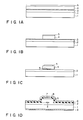
- a method of manufacturing the MT laser and its characteristics will be described below with reference to the accompanying drawings.
- Figs. 1A to 1D are sectional views schematically showing steps of manufacturing a conventional MT laser.
- etching is performed until layer 3 is exposed to form a mesa portion having a width of 15 ⁇ m.
- etching can be automatically stopped at layer 3 because of its selectivity.
- both sides of layer 3 are etched by an etchant consisting of sulfuric acid + hydrogen peroxide + water (4 : 1 : 1) to form a 1 ⁇ m-wide active region.
- an etchant consisting of sulfuric acid + hydrogen peroxide + water (4 : 1 : 1) to form a 1 ⁇ m-wide active region.
- InP is almost not etched, and only quaternary GaInAsP is etched.
- layer 5 is etched, it is etched to an extent of about 1/3 that of layer 3 because of a difference between their compositions.
- a width of the active region must be accurately controlled to be about 1 ⁇ m.
- a deep constricted portion of layer 3 etched as described above is buried with an InP layer to obtain a so-called buried hetero (BH) structure.
- BH buried hetero
- an MT technique is used to grow this buried portion. That is, a phenomenon in which the InP is first grown in the constricted portion if phosphorus is added at a high temperature (670°C). Note that if InCl3 is used as an catalyst, rapid growth can be achieved at a lower temperature.
- SiO2 film 6 as an insulating film is formed throughout the entire surface of the above element, and a window is formed at a contact portion of the insulating film.
- An AuZn layer is formed on layer 5 as p-side electrode 7 by a lift-off technique, and electrode 7 is heated and alloyed. Thereafter, Au-Cr is deposited on electrode 7 and film 6 to form electrode 8.
- n-side electrode 9 is formed on substrate 1, thereby completing the MT laser.
- electrode 7 can be formed to have a width of about 10 ⁇ m.
- the MT laser of this type has a problem of controllability with respect to a width of the active region. That is, when the 15 ⁇ m-wide active layer is to be selectively etched from the both sides to form a 1 ⁇ m-wide active region, it is difficult to stop etching of an active region at a width of 1 ⁇ m with high accuracy, and the entire active layer is sometimes etched, resulting in a poor manufacturing yield. This etching controllability becomes poor as a width of the mesa portion is increased, and a mesa width cannot be formed larger than 15 ⁇ m. Where the mesa width is 15 ⁇ m, in consideration of a mask alignment margin, a mesa width of an ohmic electrode portion must be set below 10 ⁇ m. For this reason, the contact resistance cannot be sufficiently decreased. Furthermore, since an area of the InP junction at the buried portion is defined by the width of the mesa portion, it is difficult to form the area narrower than the mesa width.
- the area of the buried portion can be adjusted by controlling a time of the MT step, controllability thereof is very poor. For this reason, the width of the buried InP junction cannot be optimized, e.g., narrowed to decrease the junction capacitance while confining the transverse mode light. Therefore, it is very difficult to obtain higher performance.
- a carrier concentration at the buried junction portion must be optimized so that the junction capacitance is decreased and a built-in potential at the junction portion is increased to decrease a current leakage, thereby obtaining a high output.
- the carrier concentration since the carrier concentration is not controlled, a concentration at the junction portion cannot be defined, resulting in a serious design problem.
- the conventional MT technique it is difficult to set the width of the active region with high accuracy, and this difficulty prevents high performance of a buried-type semiconductor light-emitting device.
- a contact area is decreased to increase the contact resistance.
- the contact area is increased, the buried area is increased to increase the junction capacitance, and it is difficult to control the width of the active region.
- an object of the present invention to provide a semiconductor light-emitting device with high performance, in which the width of the active region can be set with good controllability, the junction area and the carrier concentration of the buried portion can be optimized, the contact resistance can be decreased, and high-speed modulation can be performed, and a method of manufacturing the same.
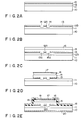
- Figs. 2A to 2E are sectional views of the respective steps for explaining a method of manufacturing a GaInAsP/InP semiconductor laser according to the first embodiment of the present invention.
- 3 ⁇ m-thick n-type InP buffer layer (first semiconductor layer) 11 is formed on n-type InP substrate 10 having a (100) crystal face as a major surface, 0.1 ⁇ m-thick undoped GaInAsP active layer (second semiconductor layer) 12 capable of emitting 1.3 ⁇ m-band light is formed on layer 11, and 0.2 ⁇ m-thick p-type InP active layer protecting layer (third semiconductor layer) 13 is formed on layer 12.
- a pair of 2 ⁇ m-wide linear grooves or stripe grooves 14 for burying are formed in second and third layers 12 and 13 by channel-etching so that a width of a finally remaining portion (active region 12a) of layer 12, sandwiched between grooves 14, becomes 1 ⁇ m.
- Grooves 14 may or may not extend into the first layer 11.
- Grooves 14 divide layer 12 into central region 12a located between them and two side portions 12b located outside them.
- a width of region 12a is preferably about 1 ⁇ m so that stable fundamental transverse mode oscillation can be obtained.
- a width of each groove 14 is preferably about 2 ⁇ m so that the transverse mode light can be sufficiently confined and the junction capacitance can be decreased.
- the widths need not be limited to the above values.
- 1.5 ⁇ m-thick p-type InP cladding layer (fourth semiconductor layer) 15 is formed on the entire surface of third layer 13 and grooves 14, so that fourth layer 15 is integral with third layer 13, and 0.8 ⁇ m-thck p+-type GaInAsP cap layer 16 is formed on layer 15.
- a pair of projections 15a of layer 15, projecting in grooves 14, are formed to sandwich a central portion (active region 12a) of the active layer.
- LPE liquid-phase epitaxial
- Au-Zn electrode 17 is formed on layer 16 in a 25 ⁇ m-wide stripe manner by a lift-off technique. Electrode 17 is alloyed by a heat treatment to ohmic-contact layer 16, and both side portions of third and fourth layers 13 and 15 are etched using electrode 17 as a mask until the upper surfaces of side portions 12b of layer 12 are exposed. If hydrochloric acid is used as an etchant during removal of layers 13 and 15, etching is accurately stopped at the upper surface of side portions 12b by its etching selectivity.
- SiO2 film 18 is deposited on first layer 11 and an outer circumference of the mesa portion. In this case, a space between first and third layers 11, 13 is kept to be located between insulating film 18 and projection 15a. A window is formed by etching at a central portion of insulating film 18 located on the upper surface of the mesa portion to expose electrode 17. Then, Au-Cr electrode 19 is deposited on the entire surface of film 18 and the exposed portion of electrode 19. In addition, a lower portion of the resultant structure is polished until the thickness of substrate 10 becomes about 100 ⁇ m, and Au-Ge electrode 20 is formed as an n-side electrode on the polished surface, thereby completing a buried-type semiconductor laser.
- widths of region 12a and the buried portion can be controlled to be design sizes with good reproducibility.
- a width of electrode 17 can be set to be 25 ⁇ m to obtain sufficient ohmic contact throughout a wide area, and the contact resistance can be sufficiently decreased. Therefore, widths of the active region and the buried portion can be optimized, thereby improving the element characteristics.
- the manufacturing yield of the element can be improved.
- the width of the constricted portion or buried portion of the mesa portion can be narrowed, the stray capacitance can be decreased, and the response characteristics can be improved to realize high-speed modulation.
- unlike in the MT technique since crystal growth need not be performed in a narrow gap portion but can be performed in a state near a planar state, stress can be eliminated and reliability can be improved.
- the width of the active layer is defined by utilizing a phenomenon that a semiconductor layer is substantially not grown on a narrow projection channel-uneveness on the substrate instead of etching the active layer. That is, in the second embodiment, two narrow stripe projections 24 each having a width of 2 ⁇ m and a height of 1 ⁇ m are formed parallel to each other on n-type InP substrate 10, as shown in Fig. 3A. Thereafter, as shown in Fig. 3B, 0.5 ⁇ m-thick n-type InP buffer layer 11 and 0.1 ⁇ m-thick GaInAsP active layer 12 are sequentially crystal-grown except on the upper surfaces of ridges 24. In this state, layer 12 is formed to be divided by projections 24 into central strip portions or active region 12a accurately defined by an interval between linear projections 24 and two side portions 12b located outside ridges 24.
- insulating film 18 and 25 ⁇ -wide Au-Zn electrode 17 are formed, and Au-Cr electrode 19 is deposited throughout the entire surfaces of electrode 17 and film 18.
- the lower portion of the resultant structure is polished until the thickness of substrate 10 becomes about 100 ⁇ m, and Au-Ge electrode 20 as an n-side electrode is formed on the polished surface as shown in Fig. 3F, thereby completing the buried-type laser.
- the widths of the active region and the buried portion can be controlled to be design sizes, and an area of a contact portion of layer 16 where electrode 17 is formed can be sufficiently widened. Therefore, the same effects as those of the first embodiments can be obtained.
- a width of an active region is defined by utilizing a phenomenon that a growth layer is interrupted at a stepped portion of a substrate.
- Stripe-mesa etching is performed on an upper portion of n-type InP substrate 10 having a major surface of a (100) crystal face so that stripe-shaped projection 34 is formed at a central portion thereof, as shown in Fig. 4A.
- Projection 34 is formed on the major surface of substrate 10 to have a width of about 2 ⁇ m by conventional photolithography in consideration of a resist mask and side-etching for obtaining a stripe direction of a ⁇ 011> direction, and is formed to have a height of 1.5 ⁇ m by an etchant consisting of hydrochloric acid + phosphoric acid (1 : 1).
- Layer 12 consists of a portion (active region 12a) located on the upper surface of the mesa portion and the other portions (side portions 12b). Each side portion 12b has a thickness 3 to 4 times that of region 12a and is almost not formed on the inclined side surface of the mesa portion. That is, region 12a located on the mesa portion is separated from side portions 12b by the inclined surfaces.
- 25 ⁇ m-wide SiO2 film 35 is formed on the central upper surface portion of layer 16 by the CVD method, and mesa-etching of layers 16 and 15 is performed using film 35 as a mask as shown in Fig. 4C.
- layer 16 is etched using, e.g., Br methanol to reach the upper surface of layer 15.
- hydrochloric acid is used to etch layer 15 to automatically stop etching at the upper surface of layer 12 as shown in Fig. 4C.
- portions 12b i.e., the portion other than region 12a on the upper surface of the mesa portion are removed by an etchant consisting of sulfuric acid + hydrogen peroxide + water, as shown in Fig. 4D. This etching is automatically stopped at the mesa portion since layer 12 is cut off thereat. Therefore, region 12a on the upper surface of the mesa portion is not removed.
- insulating film 35 is removed from layer 16, and Au-Zn electrode 17 is formed in this removed portion. Similar to the embodiments described above, insulating film 18, Au-Cr electrode 19, and electrode 20 are formed as shown in Fig. 4E, thereby completing the device. Note that if strain may occur in the active region formed in advance due to a heat treatment for ohmic-contacting electrode 17, electrode 17 may be formed instead of film 35 in the step shown in Fig. 4C.
- This embodiment differs from the aforementioned embodiment at the point that a step of a recess formed in a substrate is used to restrict a width of an active region, unlike the step of the projection.
- stripe groove 10b having a width of 1 ⁇ m and a depth of 1.5 ⁇ m is formed in a central portion of a major surface of n-type InP substrate 10 having a (100) crystal face as a major surface using an etchant similar to that used in the above embodiments.
- semiconductor layer 11, active layer 12, and semiconductor layers 13 and 15 are sequentially formed by a growing method similar to that in the above embodiments, as shown in Fig. 5B. Note that since a portion (active portion 12a) formed in groove 10b of layer 12 tends to be thicker than the other portions (side portions 12b) thereof, if liquidphase growth is used as a forming method for the layer 12, supersaturation of liquid-phase growth must be restricted.
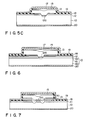
- electrodes 17, 19, and 20 and insulating film 18 are formed to complete a semiconductor laser as shown in Fig. 5C.
- n-type InP substrate is used, but a substrate in which a p-n reverse-junction is already formed may be used.
- This embodiment will be described with reference to Fig. 6.
- n-type InP body 60 is prepared, and 0.5 ⁇ m-thick p-type InP layer 61 and 0.2 ⁇ m-thick n-type InP layer 62 are sequentially liquid-phase grown on body 60, thereby obtaining substrate 10.
- a semiconductor laser is obtained by the same steps as those in the fourth embodiment described with reference to Figs. 5A to 5C.
- a p-n reverse-junction is formed between electrodes 17 and 20 in the substrate other than a portion immediately below active region 12a.
- the stray capacitance can be decreased, and a current pinching effect can be improved, so that a semiconductor laser with higher efficiency can be obtained.
- the p-n reverse-junction is formed in the substrate, but it may be formed in the mesa portion as shown in Fig. 7.
- n-type InP current confining layer 70 is interposed between p-type InP active layer protecting layer (third semiconductor layer) 13 and p-type InP cladding layer (fourth semiconductor layer) 15. Since layer 70 is not located on active region 12a, a p-n reverse-junction is formed between layer 70 and third layer 13 except on region 12a, thereby providing the same effect as that of the fifth embodiment shown in Fig. 6.
- an oxide film is used as insulating film 18, but film 18 is not limited to the oxide film.
- film 18 may be formed by heat-hardening a resin with low permittivity such as a polyimide resin.
- a resin with low permittivity such as a polyimide resin.
- the following method can be adopted.
- a non-hardened polyimide resin is coated around the mesa portion by a spin coating method, and a heat-hardening treatment is performed at a temperature of about 350°C.
- the polyimide resin has good characteristics as a filler, e.g., a specific resistance of about 10 ⁇ cm and a permittivity of about 3.5.
- the active region need not be formed with GaInAsP but may be formed with other materials, e.g., AlGaAs, or need not be formed by a single material but may be a composite layer with a layer of another material.
- the semiconductor light-emitting device is not limited to a buried-type semiconductor laser, but can be applied to, e.g., a surface light-emitting LED. In this case, a small light-emitting diameter and a wide contact area can be obtained, thereby largely improving performance.
- the semiconductor light-emitting device of the present invention since a groove or a projection around an active region is accurately defined by mask alignment, a narrow active region and a wide contact region can be obtained. For this reason, the device of the present invention can provide high-speed modulation, high efficiency, high output, and low threshold current operation with stable fundamental transverse mode oscillation, small current leakage, low resistance, and small junction capacitance.
Landscapes
- Physics & Mathematics (AREA)
- Geometry (AREA)
- Condensed Matter Physics & Semiconductors (AREA)
- General Physics & Mathematics (AREA)
- Electromagnetism (AREA)
- Optics & Photonics (AREA)
- Semiconductor Lasers (AREA)
Applications Claiming Priority (6)
| Application Number | Priority Date | Filing Date | Title |
|---|---|---|---|
| JP213800/86 | 1986-09-12 | ||
| JP21380086A JPS6370474A (ja) | 1986-09-12 | 1986-09-12 | 半導体レ−ザ素子の製造方法 |
| JP21581486A JPS6372174A (ja) | 1986-09-16 | 1986-09-16 | 埋め込み型半導体レ−ザ素子及びその製造方法 |
| JP215814/86 | 1986-09-16 | ||
| JP23185286A JPH07105556B2 (ja) | 1986-09-30 | 1986-09-30 | 半導体発光素子の製造方法 |
| JP231852/86 | 1986-09-30 |
Publications (3)
| Publication Number | Publication Date |
|---|---|
| EP0260909A2 true EP0260909A2 (de) | 1988-03-23 |
| EP0260909A3 EP0260909A3 (en) | 1988-06-01 |
| EP0260909B1 EP0260909B1 (de) | 1992-11-19 |
Family
ID=27329549
Family Applications (1)
| Application Number | Title | Priority Date | Filing Date |
|---|---|---|---|
| EP87308096A Expired - Lifetime EP0260909B1 (de) | 1986-09-12 | 1987-09-14 | Licht emittierende Halbleitervorrichtung und Verfahren zu deren Herstellung |
Country Status (3)
| Country | Link |
|---|---|
| US (2) | US4870468A (de) |
| EP (1) | EP0260909B1 (de) |
| DE (1) | DE3782704T2 (de) |
Families Citing this family (18)
| Publication number | Priority date | Publication date | Assignee | Title |
|---|---|---|---|---|
| US4870468A (en) * | 1986-09-12 | 1989-09-26 | Kabushiki Kaisha Toshiba | Semiconductor light-emitting device and method of manufacturing the same |
| US5319661A (en) * | 1990-12-27 | 1994-06-07 | The Furukawa Electric Co., Ltd. | Semiconductor double heterostructure laser device with InP current blocking layer |
| FR2695761B1 (fr) * | 1992-09-11 | 1994-12-30 | Slimane Loualiche | Procédé de fabrication de dispositifs électro-optiques à ruban, notamment de lasers, et dispositifs ainsi obtenus. |
| US5307357A (en) * | 1992-11-05 | 1994-04-26 | International Business Machines Corporation | Protection means for ridge waveguide laser structures using thick organic films |
| US5679152A (en) * | 1994-01-27 | 1997-10-21 | Advanced Technology Materials, Inc. | Method of making a single crystals Ga*N article |
| US5468656A (en) * | 1994-11-29 | 1995-11-21 | Motorola | Method of making a VCSEL |
| US5472886A (en) * | 1994-12-27 | 1995-12-05 | At&T Corp. | Structure of and method for manufacturing an LED |
| JPH1041579A (ja) * | 1996-05-21 | 1998-02-13 | Toshiba Corp | 半導体装置とその製造方法 |
| US6365968B1 (en) | 1998-08-07 | 2002-04-02 | Corning Lasertron, Inc. | Polyimide/silicon oxide bi-layer for bond pad parasitic capacitance control in semiconductor electro-optical device |
| US6577658B1 (en) | 1999-09-20 | 2003-06-10 | E20 Corporation, Inc. | Method and apparatus for planar index guided vertical cavity surface emitting lasers |
| JP2001274510A (ja) | 2000-03-28 | 2001-10-05 | Toshiba Corp | 導波路型光素子及びその製造方法 |
| US7072557B2 (en) * | 2001-12-21 | 2006-07-04 | Infinera Corporation | InP-based photonic integrated circuits with Al-containing waveguide cores and InP-based array waveguide gratings (AWGs) and avalanche photodiodes (APDs) and other optical components containing an InAlGaAs waveguide core |
| JP2005229011A (ja) * | 2004-02-16 | 2005-08-25 | Anritsu Corp | 波長可変半導体レーザ及びガス検知装置 |
| US7560739B2 (en) * | 2004-06-29 | 2009-07-14 | Intel Corporation | Micro or below scale multi-layered heterostructure |
| JP4637781B2 (ja) * | 2006-03-31 | 2011-02-23 | 昭和電工株式会社 | GaN系半導体発光素子の製造方法 |
| JP7294938B2 (ja) * | 2019-08-06 | 2023-06-20 | 日本ルメンタム株式会社 | 埋め込み型半導体光素子及びその製造方法 |
| CN115023869B (zh) * | 2020-01-28 | 2025-03-11 | 三菱电机株式会社 | 光半导体装置的制造方法 |
| JP7633771B2 (ja) * | 2020-04-02 | 2025-02-20 | 浜松ホトニクス株式会社 | 量子カスケードレーザ素子及び量子カスケードレーザ装置 |
Family Cites Families (16)
| Publication number | Priority date | Publication date | Assignee | Title |
|---|---|---|---|---|
| US3865646A (en) * | 1972-09-25 | 1975-02-11 | Bell Telephone Labor Inc | Dielectric optical waveguides and technique for fabricating same |
| JPS52104091A (en) * | 1976-02-27 | 1977-09-01 | Hitachi Ltd | Light-emitting semiconductor |
| JPS53131784A (en) * | 1977-04-22 | 1978-11-16 | Hitachi Ltd | X-ray radiation time controller |
| US4249967A (en) * | 1979-12-26 | 1981-02-10 | International Telephone And Telegraph Corporation | Method of manufacturing a light-emitting diode by liquid phase epitaxy |
| JPS57190391A (en) * | 1981-05-20 | 1982-11-22 | Nec Corp | Manufacture of semiconductor light-emitting element |
| JPS5884484A (ja) * | 1981-11-12 | 1983-05-20 | Nec Corp | 半導体レ−ザ・フオトダイオ−ド光集積化素子 |
| JPS5882587A (ja) * | 1981-11-11 | 1983-05-18 | Nec Corp | 埋め込みヘテロ構造半導体レ−ザの製造方法 |
| JPS58131785A (ja) * | 1982-01-29 | 1983-08-05 | Nec Corp | 単一軸モ−ド発振半導体レ−ザ |
| US4468850A (en) * | 1982-03-29 | 1984-09-04 | Massachusetts Institute Of Technology | GaInAsP/InP Double-heterostructure lasers |
| GB2156584B (en) * | 1984-03-16 | 1987-11-04 | Hitachi Ltd | Semiconductor laser chip |
| GB2156585B (en) * | 1984-03-16 | 1987-10-21 | Hitachi Ltd | Light-emitting device electrode |
| US4660208A (en) * | 1984-06-15 | 1987-04-21 | American Telephone And Telegraph Company, At&T Bell Laboratories | Semiconductor devices employing Fe-doped MOCVD InP-based layer for current confinement |
| US4706101A (en) * | 1984-10-27 | 1987-11-10 | Kabushiki Kaisha Toshiba | Light emitting diode formed of a compound semiconductor material |
| JPS61135181A (ja) * | 1984-12-05 | 1986-06-23 | Fujitsu Ltd | 半導体発光装置 |
| US4870468A (en) * | 1986-09-12 | 1989-09-26 | Kabushiki Kaisha Toshiba | Semiconductor light-emitting device and method of manufacturing the same |
| EP0293185B1 (de) * | 1987-05-26 | 1994-02-02 | Kabushiki Kaisha Toshiba | Halbleiterlaservorrichtung und Verfahren zu ihrer Herstellung |
-
1987
- 1987-09-11 US US07/095,114 patent/US4870468A/en not_active Expired - Lifetime
- 1987-09-14 DE DE8787308096T patent/DE3782704T2/de not_active Expired - Fee Related
- 1987-09-14 EP EP87308096A patent/EP0260909B1/de not_active Expired - Lifetime
-
1989
- 1989-07-20 US US07/382,345 patent/US4958202A/en not_active Expired - Fee Related
Also Published As
| Publication number | Publication date |
|---|---|
| US4870468A (en) | 1989-09-26 |
| DE3782704D1 (de) | 1992-12-24 |
| EP0260909A3 (en) | 1988-06-01 |
| US4958202A (en) | 1990-09-18 |
| DE3782704T2 (de) | 1993-05-06 |
| EP0260909B1 (de) | 1992-11-19 |
Similar Documents
| Publication | Publication Date | Title |
|---|---|---|
| US4660208A (en) | Semiconductor devices employing Fe-doped MOCVD InP-based layer for current confinement | |
| EP0260909B1 (de) | Licht emittierende Halbleitervorrichtung und Verfahren zu deren Herstellung | |
| EP0038085B1 (de) | Eingebettete Heterostruktur-Halbleiter-Laserdiode und Verfahren zu deren Herstellung | |
| CA2072632A1 (en) | Structure and method for fabricating indium phosphide/indium gallium arsenide phosphide buried heterostructure semiconductor lasers | |
| JPH0710016B2 (ja) | リツジ導波路半導体素子 | |
| JPH0332080A (ja) | 半導体発光素子およびその製造方法 | |
| US6865204B2 (en) | Ridge waveguide type photo semiconductor device and method for fabricating same | |
| US5222091A (en) | Structure for indium phosphide/indium gallium arsenide phosphide buried heterostructure semiconductor | |
| US4858241A (en) | Semiconductor laser device | |
| JPH05299764A (ja) | 半導体レーザの製造方法 | |
| JP2554852B2 (ja) | 半導体発光素子 | |
| JPS60251689A (ja) | 半導体レ−ザ素子及びその製法 | |
| JPS61242091A (ja) | 半導体発光素子 | |
| KR100366041B1 (ko) | 반도체레이저다이오드및그제조방법 | |
| JPS6318874B2 (de) | ||
| JP2708949B2 (ja) | 半導体レーザ装置の製造方法 | |
| JPH0983077A (ja) | 半導体光装置 | |
| JPH07105556B2 (ja) | 半導体発光素子の製造方法 | |
| JP2814124B2 (ja) | 埋込み形半導体発光素子 | |
| KR100287202B1 (ko) | 반도체레이저소자및그제조방법 | |
| JPS5914912B2 (ja) | 半導体レ−ザの製造方法 | |
| JPH0654825B2 (ja) | 半導体レーザ | |
| JPS5864086A (ja) | 埋め込みヘテロ構造半導体レ−ザ | |
| JPH01185988A (ja) | 半導体発光素子及びその製造方法 | |
| Chua et al. | Stable broad near-field (single-lateral mode) semiconductor laser |
Legal Events
| Date | Code | Title | Description |
|---|---|---|---|
| PUAI | Public reference made under article 153(3) epc to a published international application that has entered the european phase |
Free format text: ORIGINAL CODE: 0009012 |
|
| AK | Designated contracting states |
Kind code of ref document: A2 Designated state(s): DE FR GB |
|
| PUAL | Search report despatched |
Free format text: ORIGINAL CODE: 0009013 |
|
| 17P | Request for examination filed |
Effective date: 19880209 |
|
| AK | Designated contracting states |
Kind code of ref document: A3 Designated state(s): DE FR GB |
|
| 17Q | First examination report despatched |
Effective date: 19910820 |
|
| GRAA | (expected) grant |
Free format text: ORIGINAL CODE: 0009210 |
|
| AK | Designated contracting states |
Kind code of ref document: B1 Designated state(s): DE FR GB |
|
| REF | Corresponds to: |
Ref document number: 3782704 Country of ref document: DE Date of ref document: 19921224 |
|
| ET | Fr: translation filed | ||
| PLBE | No opposition filed within time limit |
Free format text: ORIGINAL CODE: 0009261 |
|
| STAA | Information on the status of an ep patent application or granted ep patent |
Free format text: STATUS: NO OPPOSITION FILED WITHIN TIME LIMIT |
|
| 26N | No opposition filed | ||
| PGFP | Annual fee paid to national office [announced via postgrant information from national office to epo] |
Ref country code: GB Payment date: 19970905 Year of fee payment: 11 |
|
| PGFP | Annual fee paid to national office [announced via postgrant information from national office to epo] |
Ref country code: DE Payment date: 19970919 Year of fee payment: 11 |
|
| PG25 | Lapsed in a contracting state [announced via postgrant information from national office to epo] |
Ref country code: GB Free format text: LAPSE BECAUSE OF NON-PAYMENT OF DUE FEES Effective date: 19980914 |
|
| REG | Reference to a national code |
Ref country code: FR Ref legal event code: D6 |
|
| GBPC | Gb: european patent ceased through non-payment of renewal fee |
Effective date: 19980914 |
|
| PG25 | Lapsed in a contracting state [announced via postgrant information from national office to epo] |
Ref country code: DE Free format text: LAPSE BECAUSE OF NON-PAYMENT OF DUE FEES Effective date: 19990701 |
|
| PGFP | Annual fee paid to national office [announced via postgrant information from national office to epo] |
Ref country code: FR Payment date: 20060908 Year of fee payment: 20 |