EP0261289B1 - Halbleiter-integrierte Anzeige - Google Patents
Halbleiter-integrierte Anzeige Download PDFInfo
- Publication number
- EP0261289B1 EP0261289B1 EP86307408A EP86307408A EP0261289B1 EP 0261289 B1 EP0261289 B1 EP 0261289B1 EP 86307408 A EP86307408 A EP 86307408A EP 86307408 A EP86307408 A EP 86307408A EP 0261289 B1 EP0261289 B1 EP 0261289B1
- Authority
- EP
- European Patent Office
- Prior art keywords
- display
- electrodes
- subset
- display electrodes
- subsets
- Prior art date
- Legal status (The legal status is an assumption and is not a legal conclusion. Google has not performed a legal analysis and makes no representation as to the accuracy of the status listed.)
- Expired
Links
- 239000004065 semiconductor Substances 0.000 title claims description 16
- 238000004519 manufacturing process Methods 0.000 claims description 13
- 229910052751 metal Inorganic materials 0.000 claims description 9
- 239000002184 metal Substances 0.000 claims description 9
- 239000011159 matrix material Substances 0.000 claims description 8
- 238000000151 deposition Methods 0.000 claims description 3
- 239000013078 crystal Substances 0.000 claims description 2
- 239000012777 electrically insulating material Substances 0.000 claims description 2
- BQCADISMDOOEFD-UHFFFAOYSA-N Silver Chemical compound [Ag] BQCADISMDOOEFD-UHFFFAOYSA-N 0.000 description 13
- 230000004888 barrier function Effects 0.000 description 13
- 229910052709 silver Inorganic materials 0.000 description 13
- 239000004332 silver Substances 0.000 description 13
- 239000004642 Polyimide Substances 0.000 description 11
- 229920001721 polyimide Polymers 0.000 description 11
- 238000000034 method Methods 0.000 description 9
- 239000000758 substrate Substances 0.000 description 7
- 239000000615 nonconductor Substances 0.000 description 6
- VYPSYNLAJGMNEJ-UHFFFAOYSA-N Silicium dioxide Chemical compound O=[Si]=O VYPSYNLAJGMNEJ-UHFFFAOYSA-N 0.000 description 4
- 239000004411 aluminium Substances 0.000 description 4
- 229910052782 aluminium Inorganic materials 0.000 description 4
- XAGFODPZIPBFFR-UHFFFAOYSA-N aluminium Chemical compound [Al] XAGFODPZIPBFFR-UHFFFAOYSA-N 0.000 description 4
- VYZAMTAEIAYCRO-UHFFFAOYSA-N Chromium Chemical compound [Cr] VYZAMTAEIAYCRO-UHFFFAOYSA-N 0.000 description 3
- XUIMIQQOPSSXEZ-UHFFFAOYSA-N Silicon Chemical compound [Si] XUIMIQQOPSSXEZ-UHFFFAOYSA-N 0.000 description 3
- 229910052804 chromium Inorganic materials 0.000 description 3
- 239000011651 chromium Substances 0.000 description 3
- 239000012212 insulator Substances 0.000 description 3
- 229910052710 silicon Inorganic materials 0.000 description 3
- 239000010703 silicon Substances 0.000 description 3
- 235000012239 silicon dioxide Nutrition 0.000 description 3
- 238000000992 sputter etching Methods 0.000 description 3
- 238000012505 colouration Methods 0.000 description 2
- 238000010276 construction Methods 0.000 description 2
- 238000005530 etching Methods 0.000 description 2
- PCHJSUWPFVWCPO-UHFFFAOYSA-N gold Chemical compound [Au] PCHJSUWPFVWCPO-UHFFFAOYSA-N 0.000 description 2
- 239000010931 gold Substances 0.000 description 2
- 229910052737 gold Inorganic materials 0.000 description 2
- 238000009413 insulation Methods 0.000 description 2
- 239000004973 liquid crystal related substance Substances 0.000 description 2
- 238000005272 metallurgy Methods 0.000 description 2
- 238000002161 passivation Methods 0.000 description 2
- 239000010453 quartz Substances 0.000 description 2
- 238000003853 Pinholing Methods 0.000 description 1
- ZLMJMSJWJFRBEC-UHFFFAOYSA-N Potassium Chemical compound [K] ZLMJMSJWJFRBEC-UHFFFAOYSA-N 0.000 description 1
- RTAQQCXQSZGOHL-UHFFFAOYSA-N Titanium Chemical compound [Ti] RTAQQCXQSZGOHL-UHFFFAOYSA-N 0.000 description 1
- 230000015572 biosynthetic process Effects 0.000 description 1
- 239000004020 conductor Substances 0.000 description 1
- 238000007796 conventional method Methods 0.000 description 1
- 230000001186 cumulative effect Effects 0.000 description 1
- 230000008030 elimination Effects 0.000 description 1
- 238000003379 elimination reaction Methods 0.000 description 1
- 230000005669 field effect Effects 0.000 description 1
- 238000002955 isolation Methods 0.000 description 1
- 229910052700 potassium Inorganic materials 0.000 description 1
- 239000011591 potassium Substances 0.000 description 1
- 239000000377 silicon dioxide Substances 0.000 description 1
- 239000010936 titanium Substances 0.000 description 1
- 229910052719 titanium Inorganic materials 0.000 description 1
Images


Classifications
-
- G—PHYSICS
- G02—OPTICS
- G02F—OPTICAL DEVICES OR ARRANGEMENTS FOR THE CONTROL OF LIGHT BY MODIFICATION OF THE OPTICAL PROPERTIES OF THE MEDIA OF THE ELEMENTS INVOLVED THEREIN; NON-LINEAR OPTICS; FREQUENCY-CHANGING OF LIGHT; OPTICAL LOGIC ELEMENTS; OPTICAL ANALOGUE/DIGITAL CONVERTERS
- G02F1/00—Devices or arrangements for the control of the intensity, colour, phase, polarisation or direction of light arriving from an independent light source, e.g. switching, gating or modulating; Non-linear optics
- G02F1/01—Devices or arrangements for the control of the intensity, colour, phase, polarisation or direction of light arriving from an independent light source, e.g. switching, gating or modulating; Non-linear optics for the control of the intensity, phase, polarisation or colour
- G02F1/15—Devices or arrangements for the control of the intensity, colour, phase, polarisation or direction of light arriving from an independent light source, e.g. switching, gating or modulating; Non-linear optics for the control of the intensity, phase, polarisation or colour based on an electrochromic effect
- G02F1/153—Constructional details
- G02F1/1533—Constructional details structural features not otherwise provided for
-
- G—PHYSICS
- G02—OPTICS
- G02F—OPTICAL DEVICES OR ARRANGEMENTS FOR THE CONTROL OF LIGHT BY MODIFICATION OF THE OPTICAL PROPERTIES OF THE MEDIA OF THE ELEMENTS INVOLVED THEREIN; NON-LINEAR OPTICS; FREQUENCY-CHANGING OF LIGHT; OPTICAL LOGIC ELEMENTS; OPTICAL ANALOGUE/DIGITAL CONVERTERS
- G02F1/00—Devices or arrangements for the control of the intensity, colour, phase, polarisation or direction of light arriving from an independent light source, e.g. switching, gating or modulating; Non-linear optics
- G02F1/01—Devices or arrangements for the control of the intensity, colour, phase, polarisation or direction of light arriving from an independent light source, e.g. switching, gating or modulating; Non-linear optics for the control of the intensity, phase, polarisation or colour
- G02F1/13—Devices or arrangements for the control of the intensity, colour, phase, polarisation or direction of light arriving from an independent light source, e.g. switching, gating or modulating; Non-linear optics for the control of the intensity, phase, polarisation or colour based on liquid crystals, e.g. single liquid crystal display cells
- G02F1/133—Constructional arrangements; Operation of liquid crystal cells; Circuit arrangements
- G02F1/136—Liquid crystal cells structurally associated with a semi-conducting layer or substrate, e.g. cells forming part of an integrated circuit
- G02F1/1362—Active matrix addressed cells
- G02F1/136277—Active matrix addressed cells formed on a semiconductor substrate, e.g. of silicon
Definitions
- the present invention relates to semiconductor integrated displays and methods of making such displays.
- European patent publication EP-A-0112417 discloses a semiconductor integrated display and method for making the same in which the display electrodes are formed from a layer of silver evaporated over the entire upper surface of a partially formed display and gaps between the individual electrodes are subsequently made by sputter etching.
- the width of the gaps between each electrode and its immediate neighbours is dictated by the need to electrically isolate each electrode from its neighbours and by the present state of the art of the technique of sputter etching.
- a further problem encountered in such displays is that of photoconduction in the semiconductor substrate. If light, which illuminates the display for viewing or projection, penetrates to the substrate, the resulting photoconduction can produce undesirable electrical leakage paths. As a result unselected areas of the display can become coloured or the colouration of selected areas of the display can fade. This problem has been recognised in the art and various proposals made to overcome it.
- One suitable method of overcoming this problem is disclosed in European patent publication EP-A-0112417 and utilises a metallic light barrier which is at least co-extensive with the gaps between the display electrodes and the semiconductor substrate.
- the present invention provides a semiconductor integrated display in which a matrix of conductive display electrodes is formed over a corresponding matrix of switching devices which is integrated in a single crystal semiconductor chip, each display electrode being connected to a respective switching device through a respective conductive path, the display electrodes being divided into a plurality of subsets each of which is formed in respective layers, so that the display electrodes of an upper subset overlap the edges of the display electrodes of a lower subset, the layers being separated by intermediate layers of electrically insulating material, the conductive paths from each higher subset passing through vias between electrodes of any lower subset and through the insulating layers to connect their respective electrodes to the corresponding switching devices.
- the display electrodes when viewed from above are suitably substantially square in shape.
- the display electrodes are suitably divided into an even number of subsets each of which is formed in respective layers, such as, for example, two or four subsets in respectively two or four layers.
- the use of four subsets enables the inter electrode gap to be completely eliminated.
- a preferred construction employs two subsets in two layers in which the alternative electrodes are arranged in the different layers to give a checkerboard arrangement. It is apparent that in such an arrangement the corners of the electrodes would be in physical and electrical contact, accordingly each electrode is produced with the corners removed. In the preferred construction the electrodes are octagonal. The removal of the corners of the electrodes results in an inter-electrode gap at each corner necessitating the employment of a metal light barrier as disclosed in European patent publication EP-A-0112417.
- the invention also provides a method of making such a semiconductor integrated display comprising at least the steps of forming an array of individually addressable transistors in a semiconductor wafer; forming a lower insulating film over said transistors, in which are provided vias above respective transistors for enabling electrical contact to be made; depositing electrically conductive metal in the vias to make electrical contact with the transistors; forming opaque display electrodes in contact with one subset of vias to form a lower subset of electrodes; forming an insulating film over the edges of the lower subset of electrodes; and forming opaque display electrodes over and in contact with a second subset of vias to form an upper subset of electrodes, so that the display electrodes of the upper subset overlap the display electrodes of the lower subset but are insulated from the lower subset of electrodes by the insulating film protecting their edges and optionally thereafter repeating the following step until the desired number of layers of display electrodes is formed:- forming opaque display electrodes over and in contact with a subset of vias to form a
- a metallic light barrier is incorporated prior to forming the display electrodes.
- the step for incorporating the light barrier consists essentially of depositing an opaque metal light barrier, comprising at least one metal different from that last deposited in the via, over the whole array; selectively removing the light barrier from over and around the edges of the vias; forming an upper insulating film over the entire light barrier which also insulates the edges of the light barrier from the via metal; and forming the opaque display electrodes as hereinbefore described.
- octahedral display electrodes 1, 1 ⁇ , 1 ⁇ and 1"' of the lower subset are seen to form with octahedral display electrodes 2, 2 ⁇ , 2 ⁇ and 2"' of the upper subset an apparently continuous electrode layer only exposing small areas 20 of electrical insulator at the corners where each octagon meets its neighbours.
- Figure 2 shows a silicon substrate 7 upon which is formed, by integrated circuit techniques, the display electrode structure of the display structure of the present invention.
- the substrate 7 has formed therein by conventional N-channel field effect transistor techniques an array of FET's.
- Each drain of a FET is connected to an overlying silver display electrode 1,2 by means of aluminium drain contact pads 4 and intermediate through via metallurgy 3 comprising a lower layer of titanium, an intermediate layer of gold and an upper layer of chromium (not shown separately).
- the FET's are connected, conventionally, by a further pattern of aluminium conductors (not shown) to row and column drivers formed at the periphery of the array.
- the drivers operate to write and to erase display electrodes selected by the contents of row and column shift registers, also formed in the silicon substrate at the periphery of the array.
- the electrical arrangement and operation of such matrix addressing and drive circuitry for an electrochromic display is described in European patent publication EP-A-42893.
- the first of these is a conventional silicon dioxide (quartz) passivation layer 6 by which the contact pads 4 and the other aluminium conduction lines are originally covered. Because such quartz insulators are susceptible to pinholing, a further organic passivation layer 8 of polyimide is also provided.
- a metallic light barrier 5 consisting of a lower thicker layer of aluminium and an upper thinner layer of chromium (not separately shown).
- a further layer 9 of polyimide to insulate the light barrier 5 from the overlying display electrode 1,2.
- the silver display electrode 1 in the lower subset of electrodes is a layer of evaporated silver. Over the edge 10 of the electrode 1 is a further layer 11 of polyimide to insulate the electrode 1 from the overlapping silver display electrode 2 in the upper subset of electrodes.
- the silver display electrode 2 is a layer of evaporated silver.
- the display electrodes 1,2 may have an additional layer of silver electroplated onto the evaporated silver layer. The surface of the display electrodes will in that case be rough to give a matt white appearance.
- the display partly illustrated has 96,000 display electrodes (pels) at a density of about 20 pels mm ⁇ 1.
- the only gap that appears between the active pels is the 4 ⁇ m ⁇ 4 ⁇ m square 20 at the corners of the pels.
- a 28 ⁇ m pel pitch design thus gives a 98% active pel area.
- a display of the type disclosed in European patent publication EP-A-011247 having a 28 ⁇ m pel pitch and a 3 ⁇ m etched gap between adjacent pels has an active pel area of 80%.
- the final active pel size is determined by the size of the pel mask for the upper subset of pels 2, 2 ⁇ , 2 ⁇ , 2"'; this is made so that the upper and lower pels are of the same size.
- the upper pel 2, 2 ⁇ , 2 ⁇ , 2"' size is therefore the same size as the pel pitch.
- the lower pels 1, 1 ⁇ , 1 ⁇ , 1"' are made 4 ⁇ m larger to provide a 2 ⁇ m per side overlap 10.
- the polyimide insulation layer 9 is baked at 250°C, after which the chromium on top of via metal 3 is etched in alkaline potassium ferrycyanide. This etch exposes bare gold at the bottom of the via.
- Silver is evaporated over the surface of the structure and patterned using a mask to define the shape of the electrodes 1 in the lower subset to give the structure shown in Figure 5.
- Figure 6 shows the pattern of silver electrodes 1 on the background polyimide insulator 9.
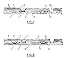
- a further layer 11 of polyimide is applied to the whole surface of the wafer, and by application of a suitable etch mask, etching the polyimide and removing the mask, vias 12 through layers 11, 9 and 8 are produced communicating with the via metal 13 as shown in Figure 7.
- the upper layer of polyimide and the via metal 13 is then treated as hereinbefore defined.
- Silver is evaporated over the surface of the structure and is patterned using a mask to define the shape of the electrode 2 in the upper subset to give the structure shown in Figure 8.
- Figure 9 shows the pattern of silver electrodes 2 on the background polyimide insulator 11.
- the display electrodes 24, 28, 32, 36 in a four layer display in which the display electrodes are in four subsets are each connected to a via 26, 30, 34, 38 respectively which in turn connects to a FET (not shown).
- Figure 11 shows the first layer of pels 24 in the four layer display each connected to a via 26 and separated from each other by electrical insulator 25.
- Figure 12 shows the second layer of pels 28 each connected to a via 30 and separated from each other by electrical insulator 29.
- Figure 13 shows the third layer of pels 32 each connected to a via 34 and separated from each other by electrical insulator 33.
- Figure 14 shows the fourth layer of pels 36 each connected to a via 38 and separated from each other by electrical insulator 37.
- Each layer of pels is fabricated in analogous manner to that illustrated herein with reference to Figures 4, 5, 7 and 8.
- the electrical insulator above the pels 24, 28 and 32 in the first, second and third subsets is etched away to leave the structure illustrated in Figure 10 showing the display electrodes in the four layers as viewed from above as a continuous surface. In the fabrication itself the vias 26, 30, 34 and 38 would not be visible through the display electrode.
Landscapes
- Physics & Mathematics (AREA)
- Nonlinear Science (AREA)
- General Physics & Mathematics (AREA)
- Optics & Photonics (AREA)
- Engineering & Computer Science (AREA)
- Microelectronics & Electronic Packaging (AREA)
- Mathematical Physics (AREA)
- Chemical & Material Sciences (AREA)
- Crystallography & Structural Chemistry (AREA)
- Devices For Indicating Variable Information By Combining Individual Elements (AREA)
- Liquid Crystal (AREA)
Claims (8)
- Integrierte Halbleiteranzeige, bei welcher eine Matrix leitender Anzeigeelektroden (1,2) über einer entsprechenden Matrix von Schaltbauelementen ausgebildet ist, die in einem Einkristallhalbleiterchip integriert ist, wobei jede Anzeigeelektrode (1, 2) mit einem entsprechenden Schaltbauelement durch eine entsprechende leitende Bahn (3, 4) verbunden ist, die Anzeigeelektroden (1, 2) in eine Mehrzahl von Untersätzen geteilt sind, bei welchen jeder in entsprechenden Schichten so ausgebildet ist, daß die Anzeigeelektroden (2) eines oberen Untersatzes die Ränder (10) der Anzeigeelektroden (1) des unteren Untersatzes überlappen, die Schichten durch Zwischenschichten eines elektrisch isolierenden Materials (11) getrennt sind, und sich die leitenden Bahnen aus jedem höheren Untersatz durch Durchgänge (12) zwischen Elektroden (1) irgendeines unteren Untersatzes und durch die isolierenden Schichten (8,9,11) erstrecken, um ihre entsprechenden Elektroden mit den entsprechenden Schaltbauelementen zu verbinden.
- Anzeige nach Anspruch 1, bei welcher die Anzeigeelektroden (1, 2) im wesentlichen quadratisch sind.
- Anzeige nach Anspruch 1 oder 2, bei welcher die Anzeigeelektroden in eine gerade Anzahl von Untersätzen geteilt sind.
- Anzeige nach irgendeinem der Ansprüche 1 bis 3, bei welcher sich die Anzeigeelektroden in zwei Untersätzen befinden.
- Anzeige nach Anspruch 4, bei welcher die Elektroden in den verschiedenen Schichten angeordnet sind, um eine Schachbrettanordnung zu ergeben und bei welcher jede Elektrode die Form eines Quadrats mit entfernten Ecken aufweist.
- Anzeige nach Anspruch 5, bei welcher die Elektroden achteckig sind.
- Anzeige nach irgendeinem der Ansprüche 1 bis 3, bei welcher sich die Anzeigeelektroden in vier Untersätzen befinden.
- Verfahren zum Herstellen einer integrierten Halbleiteranzeige nach Anspruch 1, das ein Verfahren zum Herstellen einer integrierten Halbleiteranzeige mit zumindest den folgenden Schritten umfaßt: Bilden einer Anordnung einzeln adressierbarer Transistoren in einem Halbleiterplättchen (7), Bilden einer unteren isolierenden Schicht (6, 8, 9) über den Transisitoren, in der Durchgänge oberhalb entsprechender Transisitoren vorgesehen sind, um es zu ermöglichen, einen elektrischen Kontakt herzustellen; Aufbringen elektrisch leitenden Metalls in den Durchgängen, um einen elektrischen Kontakt mit den Transistoren herzustellen; und Bilden undurchsichtiger Anzeigeelektroden in Kontakt mit einem Untersatz von Durchgängen, um einen unteren Untersatz von Elektroden (1) zu bilden; Bilden einer isolierenden Schicht (11) über den Rändern des unteren Untersatzes von Elektroden und Bilden undurchsichtiger Anzeigeelektroden über und in Kontakt mit einem zweiten Untersatz von Durchgängen (12), um einen oberen Untersatz von Elektroden (2) so zu bilden, daß die Anzeigeelektroden (2) des oberen Untersatzes die Anzeigeelektroden (1) des unteren Untersatzes überlappen, jedoch von dem unteren Untersatz von Elektroden durch die isolierende Schicht (11) isoliert sind, die ihre Ränder schützt und danach nach Wahl Wiederholen des folgenden Schritts solange, bis die gewünschte Anzahl von Schichten von Anzeigeelektroden gebildet wird,
Bilden undurchsichtiger Anzeigeelektroden über und in Kontakt mit einem Untersatz von Durchgängen, um einen Untersatz von Elektroden zu bilden, welche die Anzeigeelektroden in den unteren Untersätzen teilweise überlappen, jedoch von den unteren Untersätzen isoliert sind.
Priority Applications (4)
| Application Number | Priority Date | Filing Date | Title |
|---|---|---|---|
| EP86307408A EP0261289B1 (de) | 1986-09-26 | 1986-09-26 | Halbleiter-integrierte Anzeige |
| DE8686307408T DE3684150D1 (de) | 1986-09-26 | 1986-09-26 | Halbleiter-integrierte anzeige. |
| JP62127280A JPS6385687A (ja) | 1986-09-26 | 1987-05-26 | 半導体集積型表示装置 |
| US07/307,189 US4910579A (en) | 1986-09-26 | 1989-02-01 | Semiconductor integrated display device with overlapping electrodes |
Applications Claiming Priority (1)
| Application Number | Priority Date | Filing Date | Title |
|---|---|---|---|
| EP86307408A EP0261289B1 (de) | 1986-09-26 | 1986-09-26 | Halbleiter-integrierte Anzeige |
Publications (2)
| Publication Number | Publication Date |
|---|---|
| EP0261289A1 EP0261289A1 (de) | 1988-03-30 |
| EP0261289B1 true EP0261289B1 (de) | 1992-03-04 |
Family
ID=8196157
Family Applications (1)
| Application Number | Title | Priority Date | Filing Date |
|---|---|---|---|
| EP86307408A Expired EP0261289B1 (de) | 1986-09-26 | 1986-09-26 | Halbleiter-integrierte Anzeige |
Country Status (4)
| Country | Link |
|---|---|
| US (1) | US4910579A (de) |
| EP (1) | EP0261289B1 (de) |
| JP (1) | JPS6385687A (de) |
| DE (1) | DE3684150D1 (de) |
Families Citing this family (6)
| Publication number | Priority date | Publication date | Assignee | Title |
|---|---|---|---|---|
| US5042918A (en) * | 1988-11-15 | 1991-08-27 | Kabushiki Kaisha Toshiba | Liquid crystal display device |
| JPH02192146A (ja) * | 1989-01-20 | 1990-07-27 | Toshiba Corp | 半導体装置 |
| US5657150A (en) * | 1993-09-10 | 1997-08-12 | Eyeonics Corporation | Electrochromic edge isolation-interconnect system, process, and device for its manufacture |
| JP3349332B2 (ja) * | 1995-04-28 | 2002-11-25 | インターナショナル・ビジネス・マシーンズ・コーポレーション | 反射式空間光変調素子配列及びその形成方法 |
| US5818564A (en) * | 1996-09-13 | 1998-10-06 | Raychem Corporation | Assembly including an active matrix liquid crystal display module |
| US6246459B1 (en) | 1998-06-10 | 2001-06-12 | Tyco Electronics Corporation | Assembly including an active matrix liquid crystal display module and having plural environmental seals |
Family Cites Families (11)
| Publication number | Priority date | Publication date | Assignee | Title |
|---|---|---|---|---|
| JPS5532897B2 (de) * | 1973-03-16 | 1980-08-27 | ||
| US4239346A (en) * | 1979-05-23 | 1980-12-16 | Hughes Aircraft Company | Compact liquid crystal display system |
| JPS5710273A (en) * | 1980-06-20 | 1982-01-19 | Hitachi Ltd | Photosensor array device |
| JPS5720778A (en) * | 1980-07-11 | 1982-02-03 | Matsushita Electric Industrial Co Ltd | Image display unit |
| JPS5727046A (en) * | 1980-07-25 | 1982-02-13 | Seiko Epson Corp | Semiconductor device |
| JPS58222546A (ja) * | 1982-04-13 | 1983-12-24 | Citizen Watch Co Ltd | 半導体装置 |
| JPS58223173A (ja) * | 1982-06-21 | 1983-12-24 | シャープ株式会社 | ドツトマトリツクス型表示装置 |
| EP0112417A1 (de) * | 1982-12-22 | 1984-07-04 | International Business Machines Corporation | Integrierte Anzeigevorrichtung mit Halbleiterschaltung und Verfahren zur Herstellung einer solchen Vorrichtung |
| US4639087A (en) * | 1984-08-08 | 1987-01-27 | Energy Conversion Devices, Inc. | Displays having pixels with two portions and capacitors |
| JPS61193479A (ja) * | 1985-02-22 | 1986-08-27 | Fuji Photo Film Co Ltd | 固体カラ−撮像デバイス |
| JPS622566A (ja) * | 1985-06-28 | 1987-01-08 | Toshiba Corp | 固体撮像装置 |
-
1986
- 1986-09-26 DE DE8686307408T patent/DE3684150D1/de not_active Expired - Lifetime
- 1986-09-26 EP EP86307408A patent/EP0261289B1/de not_active Expired
-
1987
- 1987-05-26 JP JP62127280A patent/JPS6385687A/ja active Pending
-
1989
- 1989-02-01 US US07/307,189 patent/US4910579A/en not_active Expired - Fee Related
Also Published As
| Publication number | Publication date |
|---|---|
| DE3684150D1 (de) | 1992-04-09 |
| JPS6385687A (ja) | 1988-04-16 |
| EP0261289A1 (de) | 1988-03-30 |
| US4910579A (en) | 1990-03-20 |
Similar Documents
| Publication | Publication Date | Title |
|---|---|---|
| US5828433A (en) | Liquid crystal display device and a method of manufacturing the same | |
| KR100321925B1 (ko) | 4장의마스크를이용한액정표시장치용박막트랜지스터기판의제조방법및액정표시장치용박막트랜지스터기판 | |
| KR100264112B1 (ko) | 액티브 매트릭스 기판 및 그 제조 방법 | |
| US5017984A (en) | Amorphous silicon thin film transistor array | |
| US4816885A (en) | Thin-film transistor matrix for liquid crystal display | |
| JP4169811B2 (ja) | 薄膜トランジスタの製造方法 | |
| KR20040007247A (ko) | 엑스레이 검출 배열 소자를 제작하는 방법 | |
| KR100531046B1 (ko) | 엑스레이 검출 배열 소자를 제작하는 방법 | |
| EP0261289B1 (de) | Halbleiter-integrierte Anzeige | |
| KR0169356B1 (ko) | 박막트랜지스터 액정 디스플레이 소자 및 그 제조방법 | |
| JPH07114281B2 (ja) | ドライバ−内蔵アクティブマトリックス基板 | |
| JP2806740B2 (ja) | 液晶表示装置およびその製造方法 | |
| KR100537882B1 (ko) | 액정표시장치및그제조방법 | |
| US5523866A (en) | Liquid-crystal display device having slits formed between terminals or along conductors to remove short circuits | |
| US20110129952A1 (en) | Thin film transistor substrates and method of manufacturing the same | |
| KR100283519B1 (ko) | 액정 표시 장치용 박막 트랜지스터 기판의 제조 방법 | |
| KR100438964B1 (ko) | 액정표시장치및그제조방법 | |
| KR100267993B1 (ko) | 액정표시장치와그제조방법 | |
| KR100315914B1 (ko) | 4장의마스크를이용한액정표시장치용박막트랜지스터기판의제조방법및액정표시장치용박막트랜지스터기판 | |
| KR100262406B1 (ko) | 액정 표시 소자 및 그 제조방법 | |
| KR100236023B1 (ko) | 액정 표시장치 | |
| KR100552300B1 (ko) | 액정 표시 장치용 박막 트랜지스터 기판의 제조 방법 | |
| US20020047949A1 (en) | Liquid crystal displays | |
| JPH09325361A (ja) | アクティブマトリクス基板の製造方法 | |
| KR20000026540A (ko) | 4장의 마스크를 이용한 액정 표시 장치용 박막 트랜지스터 기판의 제조 방법 및 액정 표시 장치용박막 트랜지스터 기판 |
Legal Events
| Date | Code | Title | Description |
|---|---|---|---|
| PUAI | Public reference made under article 153(3) epc to a published international application that has entered the european phase |
Free format text: ORIGINAL CODE: 0009012 |
|
| AK | Designated contracting states |
Kind code of ref document: A1 Designated state(s): DE FR GB |
|
| 17P | Request for examination filed |
Effective date: 19880729 |
|
| 17Q | First examination report despatched |
Effective date: 19901107 |
|
| GRAA | (expected) grant |
Free format text: ORIGINAL CODE: 0009210 |
|
| AK | Designated contracting states |
Kind code of ref document: B1 Designated state(s): DE FR GB |
|
| REF | Corresponds to: |
Ref document number: 3684150 Country of ref document: DE Date of ref document: 19920409 |
|
| ET | Fr: translation filed | ||
| PG25 | Lapsed in a contracting state [announced via postgrant information from national office to epo] |
Ref country code: GB Effective date: 19920926 |
|
| PLBE | No opposition filed within time limit |
Free format text: ORIGINAL CODE: 0009261 |
|
| STAA | Information on the status of an ep patent application or granted ep patent |
Free format text: STATUS: NO OPPOSITION FILED WITHIN TIME LIMIT |
|
| 26N | No opposition filed | ||
| GBPC | Gb: european patent ceased through non-payment of renewal fee |
Effective date: 19920926 |
|
| PG25 | Lapsed in a contracting state [announced via postgrant information from national office to epo] |
Ref country code: FR Effective date: 19930528 |
|
| PG25 | Lapsed in a contracting state [announced via postgrant information from national office to epo] |
Ref country code: DE Effective date: 19930602 |
|
| REG | Reference to a national code |
Ref country code: FR Ref legal event code: ST |