EP0262413A1 - Dispositif de mémoire à multiplexage d'adresses - Google Patents
Dispositif de mémoire à multiplexage d'adresses Download PDFInfo
- Publication number
- EP0262413A1 EP0262413A1 EP87112567A EP87112567A EP0262413A1 EP 0262413 A1 EP0262413 A1 EP 0262413A1 EP 87112567 A EP87112567 A EP 87112567A EP 87112567 A EP87112567 A EP 87112567A EP 0262413 A1 EP0262413 A1 EP 0262413A1
- Authority
- EP
- European Patent Office
- Prior art keywords
- address
- counter
- memory device
- supplied
- buffer
- Prior art date
- Legal status (The legal status is an assumption and is not a legal conclusion. Google has not performed a legal analysis and makes no representation as to the accuracy of the status listed.)
- Granted
Links
Images






Classifications
-
- G—PHYSICS
- G11—INFORMATION STORAGE
- G11C—STATIC STORES
- G11C8/00—Arrangements for selecting an address in a digital store
-
- G—PHYSICS
- G11—INFORMATION STORAGE
- G11C—STATIC STORES
- G11C7/00—Arrangements for writing information into, or reading information out from, a digital store
- G11C7/10—Input/output [I/O] data interface arrangements, e.g. I/O data control circuits, I/O data buffers
- G11C7/1015—Read-write modes for single port memories, i.e. having either a random port or a serial port
- G11C7/1018—Serial bit line access mode, e.g. using bit line address shift registers, bit line address counters, bit line burst counters
-
- G—PHYSICS
- G11—INFORMATION STORAGE
- G11C—STATIC STORES
- G11C8/00—Arrangements for selecting an address in a digital store
- G11C8/04—Arrangements for selecting an address in a digital store using a sequential addressing device, e.g. shift register, counter
Definitions
- the present invention generally relates to memory devices employing address multiplexing, and more particularly to a memory device employing address multiplexing and comprising a counter which generates an address of a column decoder responsive to toggle of a column address strobe (CAS).
- CAS column address strobe
- a plurality of inverted column address strobes (hereinafter simply referred to as CAS) are entered for one active time period of an inverted row address strobe (hereinafter simply referred to as a RAS), so that the writing and reading of data to memory cells can be carried out at a high speed.
- RAS inverted row address strobe
- access is made to the memory cells designated by a row address which is set when the RAS is made active, by successively entering a column address and the CAS in a state where the RAS is maintained active. Since the access is made to the memory cells without changing the row address, there is no address selection time nor resetting time for the row selection, and it is thus possible to obtain a quick access time and a short cycle time.
- Another and more specific object of the present invention is to provide a memory device employing address multiplexing and comprising a counter.
- An external address is initially set in the counter and a counted address value is incremented responsive to toggle of a column address strobe.
- the counted address value in the counter is supplied as an address signal directly to a column decoder or indirectly to the column decoder through an address buffer.
- the memory device of the present invention it is possible to carry out the writing and reading operation at a high speed as in the case of a nibble mode.
- the circuit construction is simple and an area occupied by circuit parts constituting the memory device is small compared to that of the conventional memory device.
- Still another object of the present invention is to provide a memory device employing the address multiplexing and comprising a counter and a switching logic circuit.
- An external address is initially set in the counter and a counted address value is incremented responsive to toggle of a column address strobe.
- the counted address value in the counter is supplied as an address signal directly to a column decoder or indirectly to the column decoder through an address buffer.
- the switching logic circuit switches the address bits in the counter depending on information such as bonding information, information concerning the melting of a fuse and information related to aluminum wiring. According to the memory device of the present invention, it is possible to arbitrarily determine which address bits in the counter are to determine a nibble address. Hence, it is possible to use the same counter to generate the nibble address for memory device having different memory structures.
- FIGS.1 (A) through 1 (D) are timing charts for explaining the operation of the conventional memory device described before in the page mode, where "Col. Addr” denotes the column address, “Row Addr” denotes the row address, and Dour denotes the output.
- FIGS.2(A) through 2(D) are timing charts for explaining the operation of the conventional memory device described before in the nibble mode, where the same designations are used as in FIGS.1 (A) through 1 (D).
- a plurality of the CAS are entered for one active time period of the RAS, so that the writing and reading of data to memory cells can be carried out at a high speed.
- access is made to the memory cells designated by a row address which is set when the RAS is made active, by successively entering a column address and the CAS in a state where the RAS is maintained active.
- FIG.3 shows an essential part of the conventional 64 K dynamic random access memory (DRAM) having the nibble mode.
- DRAM dynamic random access memory
- the 4 bits of stored data from the memory cells are supplied to sense and latch circuits 11, through 11 4 in parallel through the respective data bus pairs 10, through 10 4 .
- An initial content is set in a nibble shift register 12, and the content of the nibble shift register 12 is successively shifted responsive to the toggle of the CAS.
- the 4 bits of data are successively latched in the sense and latch circuits 11, through 11 4 and are sequentially outputted as the output Dour from an output buffer 13 responsive to an output of the nibble shift register 12.
- the serial output Dour is obtained through a terminal 14.
- a serial input D IN is applied to a terminal 15 and is supplied to an input buffer 16.
- the input buffer 16 supplies the serial input D, N as parallel 4 bit data to write-in buffers 17, through 17 d , and the write-in buffers 17, through 17 4 successively supply the 4 bit parallel data to the memory cells through the respective data bus pairs 10, through 10 4 responsive to the output of the nibble shift register 12.
- the 4 bit data on the data bus pairs 10, through 10A are latched by the sense and latch circuits 11 1 through 11 4 . Accordingly, during one active time period of the RAS in the nibble mode, the stored data may be rewritten or the write-in data which is written may be read out.
- the present invention eliminates these problems of the conventional memory device by providing a counter which generates an address of a column decoder responsive to toggle of the CAS in the nibble mode.
- the term “nibble” is used to indicate half byte or 4 bits.
- the scope of the present invention is not limited to the conventional nibble mode, and for this reason, the term “nibble” is used in a more broader sense in the present specification and is not limited to 4 bits as will be described later on in the present specification.
- FIG.4 shows an essential part of a first embodiment of the memory device according to the present invention for explaining the operating principle thereof.
- ADD denotes an external address
- ⁇ denotes a clock signal for setting the column address of the external address ADD in an address buffer 22. This clock signal ⁇ is generated responsive to a falling edge of the CAS.
- FIGS.5(A) through 5(C) are timing charts for explaining the operation of the block system shown in FIG.4.
- the column address of the external address ADD is set in a nibble counter 21 as shown in FIG.5(C).
- the operation of setting this column address is carried out responsive to the clock signal ⁇ .
- the external address ADD may be set in the nibble counter 21 through the address buffer 22 as indicated by solid line (a), or the column address may be set directly in the nibble counter 21 as indicated by phantom line (b).
- the nibble counter 21 counts up responsive to a nibble clock signal ⁇ NBC .
- the address in the nibble counter 21 is obtained in the next nibble cycle, and a column decoder (not shown) is operated.
- the address from the nibble counter 21 may be supplied to the column decoder after being amplified in the address buffer 22 as indicated by solid line (c), or the address from the nibble counter 21 may be supplied directly to the column decoder as indicated by phantom line (d).
- the counted address value in the nibble counter 21 is incremented responsive to the nibble clock signal ⁇ NBC .
- the data read-out speed is slowed down by an amount corresponding to the time it takes to initially set the external address ADD.
- it is possible to reduce the number of data bus pairs, the sense and latch circuits, and the write-in buffers compared to the conventional memory device.
- the area occupied by the data bus pairs and the circuit parts is reduced compared to that of the conventional memory device.
- These advantages become particularly notable as the number of parallel input and output bits becomes large.
- 4 bits are outputted by the toggle of the CAS in the nibble mode of the conventional memory device, but according to the present embodiment, it is possible to output a larger number of bits by increasing the number of bits of the nibble counter 21.
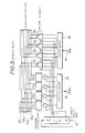
- FIG.6 shows a more detailed construction of the first embodiment
- FIG.7 shows an embodiment of the circuit construction of the nibble counter 21 and the address buffer 22 for one address bit.
- the memory device generally comprises the nibble counter 21, the address buffer 22, a memory cell array 23 having a matrix arrangement of memory cells (not shown) each designated by a row address and a column address, a column decoder 24, a sense and latch circuit 25 for 4 bits, a write-in buffer 26 for 4 bits, an output buffer 27, and a data bus 28.
- the address buffer 22 comprises a flip-flop FF, inverters 40 through 42, and N-channel transistors Q N4 and Q N5 .
- the flip-flop FF comprises P-channel transistors Qp 1 through Qp 4 and N-channel transistors Q N1 through Q N3 .
- the nibble counter 21 comprises a transfer gate TG constituted by N-channel transistors Q N6 and Q N7 , N-channel transistors Q N8 and Q N9 , a master flip-flop MFF and a slave flip-flop SFF.
- the master flip-flop MFF comprises inverters 43 and 44, and N-channel transistors Q N10 through Q N13 .
- the slave flip-flop SFF comprises inverters 45 and 46, and P-channel transistors Qp 5 through Q P8 .
- Vcc denotes a power source voltage.
- the nibble counter 21 has the function of initially entering the first bit from the external address ADD.
- the address buffer 22 is provided with the flip-flop FF and stores the first address bit responsive to a latch enable clock signal ⁇ LE .
- the nibble counter 21 is provided with the master flip-flop MFF and the slave flip-flop SFF which operate alternately.
- the data at nodes N 1 and N 2 in the address buffer 22 is set to nodes N 3 and N 4 in the slave flip-flop SFF by the operation of transistors Q NB and Q N9 .
- a signal ⁇ AL is controlled so that the data is only set the first time.
- the level of a control clock signal ⁇ T for the transfer gate TG in the nibble counter 21 is raised so as to output counter information Q and Q from the nibble counter 21 to the nodes N 1 and N 2 in the address buffer 22.
- the counted address value of the nibble counter 21 is incremented responsive to a clock signal ⁇ CLK , and the counter information Q and Q are successively outputted.
- the circuit parts shown correspond only to one bit of the nibble counter 21 and the address buffer 22.
- the nibble counter 21 and the address buffer 22 actually comprise circuit parts corresponding to a predetermined number of bits required to set the external address ADD.
- the circuit parts actually provided correspond to 2 bits of the address which is varied. It is possible to provide circuit parts corresponding to more than 2 bits, but the address portion of the bits provided in addition to the 2 bits is not varied.
- FIG.8 shows an embodiment of the connection of counters constituting the nibble counter 21.
- the nibble counter 21 comprises a plurality of counter elements 30 1 , 30 2 , 30 3 , ... (only three shown) in correspondence with each bit of the nibble counter 21, an inverter INV, and a plurality of NAND circuits 31 1 , 31 2 , 31 3 , ... (only three shown).
- Each NAND circuit determines whether or not to take a figure up one place based on the information from the counter in the previous stage.
- FIG.9 shows an embodiment of a clock generating circuit for generating signals which control the block system shown in FIG.6.
- the clock generating circuit comprises delay circuits 32 through 35, NOR circuits 36 through 39, inverters 48, through 48 2 , and an OR circuit 49.
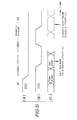
- FIGS.10(E), 10(F), 10(1) and 10(J) respectively show signals ⁇ LE , ⁇ AL , ⁇ T and ⁇ NBC .
- the first external address ADD is entered into the nibble counter 21 responsive to the signal ⁇ AL during a time t 1
- the counted address value is incremented responsive to the nibble clock signal ⁇ NBC during a time t 2
- the address is outputted from the nibble counter 21 during a time t 3
- the counted address value is incremented responsive to the nibble clock signal ⁇ NBC during a time t A .
- the clock generating circuit produces the signal ⁇ AL by using a time interval between a falling edge of the signal at the node 1 and a falling edge of the signal at the node 5.
- the external address ADD is entered into the address buffer 22 responsive to the signal ⁇ AL shown in FIG.10(F) and is latched responsive to the latch enable clock signal ⁇ LE shown in FIG.10(E).
- the latched address is outputted as addresses A and A to determine the first bit of the column address.
- control clock signal OT shown in FIG.10(1) is produced responsive to the fall in the signal at the node 8 shown in FIG.10(G) and the second and subsequent toggles of the CAS shown in FIG.10(B).
- the nibble clock signal ⁇ NBC is produced by delaying a logical sum of the signals ⁇ AL and ⁇ T .
- the data in the slave flip-flop SFF is transferred to the master flip-flop MFF during the high-level period of the control clock signal ⁇ T
- the data in the master flip-flop MFF is transferred to the slave flip-flop SFF during the low-level period of the control clock signal ⁇ T .
- the clock signal ⁇ CLK described before is produced by carrying out a NAND operation between the nibble clock signal ⁇ NBC and an output of the counter in the previous stage in FIG.B. Hence, the nibble counter 21 increments the count responsive to the clock signal ⁇ CLK in FIG.7.
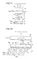
- FIG.11 shows an essential part of the second embodiment for explaining the operating principle thereof.
- the memory device additionally comprises a switching logic circuit 51, and switching information I sw is supplied to the switching logic circuit 51.
- the switching information I s w relates to bonding option (or information), information concerning the melting of a fuse, information related to aluminum wiring and the like.
- the timings of the RAS, CAS and the address are the same as those shown in FIGS.5-(A) through 5(C).
- the bits of data related to the entered column and row addresses are successively outputted responsive to the toggle of the CAS, as described before.
- the nibble address is determined by a row address bit RA9 and a column address bit CA9.
- the nibble address is determined by column address bits CAO and CA1.
- the switching logic circuit 51 switches the bits of the nibble counter 21 responsive to the switching information I sw so that the nibble address can be generated from the same nibble counter 21 regardless of the memory structure of the memory device.
- FIG.13 shows a more detailed construction of the block system shown in FIG.11.
- FIG.13 shows the case where the bits determining the nibble address are switched between bits AO and A1 and bits A2 and A3.
- the other bits of the external address ADD may be stored separately in a register (not shown), for example.
- the switching logic circuit 51 comprises AND circuits ao through as and an inverter INV 2 .
- the AND circuit a o obtains a logical product of an output Q 1 of a counter element 53, corresponding to the address bit A 1 , the nibble clock signal ⁇ NBC and the switching information I sw .
- the AND circuit a obtains a logical product of an output Qo of a counter element 53o corresponding to the address bit Ao, the nibble clock signal ⁇ NBC and the switching information I sw .
- the nibble clock signal ⁇ NBC is selectively supplied to the clock terminals CLK of the counter elements 53o and 53, corresponding to the bits AO and A1 of the nibble counter 21, and the bits AO and A1 change as shown in the following Table 1 while the bits A2 and A3 remain unchanged responsive to each nibble clock signal ⁇ NBC , where 1) through 5) in the Table 1 denote the five sequential pulses of the nibble clock signal ⁇ NBC .
- the nibble clock signal ⁇ NBC is selectively supplied to the clock terminals CLK of the counter elements 53 2 and 53 3 corresponding to the bits A2 and A3 of the nibble counter 21, and the bits A2 and A3 change while the bits AO and A1 remain unchanged responsive to each nibble clock signal ⁇ NBC .
- FIG.14 is a diagram for explaining the switching of the nibble address for the case where the present embodiment is applied to a 1 Mbit memory device.
- the memory structure is selected by bonding option.
- FIG.15 is a plan view showing an integrated circuit package.
- a pin T of an integrated circuit (IC) package 55 is bonded to a bonding pad PAD on an IC chip 56 by an aluminum wire 57.
- the logic value of the switching information I sw is determined by whether or not the bonding is made. For example, the switching information I sw has a low level (logic value "0") when no bonding is made and has a high level (logic value "1") when the bonding is made by the aluminum wire 57.
- the potential at the pin T of the IC package 55 is equal to the power source voltage Vcc which is a high level
- the potential at a node N is high when the terminal T and the bonding pad PAD are bonded by the aluminum wire 57, and the switching information I sw has the high level.
- the potential at the node N is low when no bonding is made because a resistor R is connected between the node N and a ground voltage Vss which is a low level, and the switching information I sw has the low level.
- a row address bit RA and a column address bit CA are entered through a common terminal of the IC package 55.
- the row address bit RAO and the column address bit CAO are entered time-divisionally through a pin T0.
- the row address bit RA9 and the column address bit CA9 are entered on after the other in time division through a terminal T9.
- the column address bits CAO through CA9 and the row address bit RA9 are entered into the nibble counter 21 through the pins TO through T9.
- the least significant bits RA9 and CA9 determine the nibble address.
- the nibble counter 21 counts up responsive to each nibble clock signal ⁇ NBC , but only the bits RA9 and CA9 change and the remaining bits including the most significant bits CAO and CA1 remain unchanged as shown in Table 2.
- the memory is designed so that the row address bit RA9 is used for the nibble address.
- the pin T is bonded to the bonding pad PAD by the aluminum wire 57.
- the most significant bits CAO and CA1 determine the nibble address.
- the nibble counter 21 counts up responsive to each nibble clock signal ⁇ NBC , but only the bits CAO and CA1 change and the remaining bits including the least significant bits CA9 and RA9 remain unchanged as shown in Table 3.
- FIG.16 shows another embodiment of the switching logic circuit together with a part of the nibble counter.
- the nibble addresses for the 256 K ⁇ 4 bit memory device and the 1 M X 1 bit memory device decided by the Joint Electron Device Engineering Council (JEDEC) are generated by the same nibble counter.
- the switching logic circuit 51 comprises NAND circuits 60o through 60 11 , and a part of the nibble counter 21 shown comprises counters 61, through 6111.
- Clock signals ⁇ x1 and ⁇ x4 are generated from the switching information such as the bonding information.
- the nibble counter 21 outputs the address bits CAO and CAI during a high-level period of the clock signal ⁇ x4 .
- the nibble counter 21 outputs the address bits RA9 and CA9 during a high-level period of the clock signal ⁇ x1 when the level of clock signal ⁇ 4 is low.
- the present embodiment it is possible to arbitrarily select the memory structure of the 1 Mbit memory device between 1 M X 1 bit and 256 K ⁇ 4 bits by providing or not providing the bonding between the terminal and the bonding pad of the IC package, and the nibble address for the different memory structures can be generated by the same nibble counter.
- the switching information (I SW , ⁇ x1 , and ⁇ x4 ) which is used to switch the bits of the nibble counter determining the nibble address is not limited to the information related to the bonding, and may be other information such as information indicating whether or not a fuse is melted and information related to an aluminum wiring indicating whether or not an aluminum wiring is provided between specific terminals and the like.
Landscapes
- Engineering & Computer Science (AREA)
- Microelectronics & Electronic Packaging (AREA)
- Dram (AREA)
Applications Claiming Priority (4)
| Application Number | Priority Date | Filing Date | Title |
|---|---|---|---|
| JP208526/86 | 1986-09-04 | ||
| JP208527/86 | 1986-09-04 | ||
| JP61208527A JPS6364698A (ja) | 1986-09-04 | 1986-09-04 | 記憶装置 |
| JP61208526A JPS6364697A (ja) | 1986-09-04 | 1986-09-04 | 記憶装置 |
Publications (2)
| Publication Number | Publication Date |
|---|---|
| EP0262413A1 true EP0262413A1 (fr) | 1988-04-06 |
| EP0262413B1 EP0262413B1 (fr) | 1992-07-22 |
Family
ID=26516884
Family Applications (1)
| Application Number | Title | Priority Date | Filing Date |
|---|---|---|---|
| EP87112567A Expired - Lifetime EP0262413B1 (fr) | 1986-09-04 | 1987-08-28 | Dispositif de mémoire à multiplexage d'adresses |
Country Status (4)
| Country | Link |
|---|---|
| US (1) | US4807192A (fr) |
| EP (1) | EP0262413B1 (fr) |
| KR (1) | KR910006110B1 (fr) |
| DE (1) | DE3780551T2 (fr) |
Cited By (4)
| Publication number | Priority date | Publication date | Assignee | Title |
|---|---|---|---|---|
| EP0476282A3 (en) * | 1990-07-31 | 1992-06-24 | Texas Instruments Incorporated | Improvements in or relating to integrated circuits |
| EP0611026A1 (fr) * | 1993-01-05 | 1994-08-17 | STMicroelectronics, Inc. | Antémémoire de données à double porte |
| EP0755539A4 (fr) * | 1994-04-11 | 1997-11-12 | Intel Corp | Unite de memoire systeme, de cout reduit et a performances ameliorees, a memoire ram dynamique a sortie de donnees etendue |
| FR2757305A1 (fr) * | 1996-12-17 | 1998-06-19 | Sgs Thomson Microelectronics | Dispositif et procede de lecture incrementale d'une memoire |
Families Citing this family (4)
| Publication number | Priority date | Publication date | Assignee | Title |
|---|---|---|---|---|
| US5323355A (en) * | 1991-01-22 | 1994-06-21 | Fujitsu Limited | Semiconductor memory device |
| JPH0628846A (ja) * | 1992-07-09 | 1994-02-04 | Mitsubishi Electric Corp | 半導体記憶装置 |
| US6336159B1 (en) * | 1997-06-25 | 2002-01-01 | Intel Corporation | Method and apparatus for transferring data in source-synchronous protocol and transferring signals in common clock protocol in multiple agent processing system |
| KR100600053B1 (ko) * | 2004-07-27 | 2006-07-13 | 주식회사 하이닉스반도체 | 어드레스핀과 데이터핀을 공유하는 의사 에스램 |
Citations (7)
| Publication number | Priority date | Publication date | Assignee | Title |
|---|---|---|---|---|
| EP0049988A2 (fr) * | 1980-10-10 | 1982-04-21 | Inmos Corporation | Transfert de données à grande vitesse pour une mémoire semiconductrice |
| EP0080902A2 (fr) * | 1981-12-02 | 1983-06-08 | Fujitsu Limited | Dispositif de mémoire semi-conductrice |
| WO1985000920A1 (fr) * | 1983-08-08 | 1985-02-28 | Western Electric Company, Inc. | Interface d'adresses multiplexees pour l'adressage de memoires de capacites diverses |
| EP0135940A2 (fr) * | 1983-09-29 | 1985-04-03 | Nec Corporation | Circuit de mémoire à double porte |
| EP0136414A2 (fr) * | 1983-07-08 | 1985-04-10 | Texas Instruments Incorporated | Mémoire dynamique à mode séquentiel rapide |
| EP0147268A2 (fr) * | 1983-11-15 | 1985-07-03 | SAT (Société Anonyme de Télécommunications),Société Anonyme | Dispositif d'adressage de memoire |
| EP0156316A2 (fr) * | 1984-03-24 | 1985-10-02 | Kabushiki Kaisha Toshiba | Dispositif de mémoire avec commande d'accès de données |
Family Cites Families (2)
| Publication number | Priority date | Publication date | Assignee | Title |
|---|---|---|---|---|
| EP0162234A3 (fr) * | 1980-07-23 | 1986-03-19 | Nec Corporation | Dispositif de mémoire |
| US4608678A (en) * | 1983-12-23 | 1986-08-26 | Advanced Micro Devices, Inc. | Semiconductor memory device for serial scan applications |
-
1987
- 1987-08-28 EP EP87112567A patent/EP0262413B1/fr not_active Expired - Lifetime
- 1987-08-28 DE DE8787112567T patent/DE3780551T2/de not_active Expired - Fee Related
- 1987-08-31 US US07/090,988 patent/US4807192A/en not_active Expired - Lifetime
- 1987-09-04 KR KR8709797A patent/KR910006110B1/ko not_active Expired
Patent Citations (7)
| Publication number | Priority date | Publication date | Assignee | Title |
|---|---|---|---|---|
| EP0049988A2 (fr) * | 1980-10-10 | 1982-04-21 | Inmos Corporation | Transfert de données à grande vitesse pour une mémoire semiconductrice |
| EP0080902A2 (fr) * | 1981-12-02 | 1983-06-08 | Fujitsu Limited | Dispositif de mémoire semi-conductrice |
| EP0136414A2 (fr) * | 1983-07-08 | 1985-04-10 | Texas Instruments Incorporated | Mémoire dynamique à mode séquentiel rapide |
| WO1985000920A1 (fr) * | 1983-08-08 | 1985-02-28 | Western Electric Company, Inc. | Interface d'adresses multiplexees pour l'adressage de memoires de capacites diverses |
| EP0135940A2 (fr) * | 1983-09-29 | 1985-04-03 | Nec Corporation | Circuit de mémoire à double porte |
| EP0147268A2 (fr) * | 1983-11-15 | 1985-07-03 | SAT (Société Anonyme de Télécommunications),Société Anonyme | Dispositif d'adressage de memoire |
| EP0156316A2 (fr) * | 1984-03-24 | 1985-10-02 | Kabushiki Kaisha Toshiba | Dispositif de mémoire avec commande d'accès de données |
Cited By (6)
| Publication number | Priority date | Publication date | Assignee | Title |
|---|---|---|---|---|
| EP0476282A3 (en) * | 1990-07-31 | 1992-06-24 | Texas Instruments Incorporated | Improvements in or relating to integrated circuits |
| EP0611026A1 (fr) * | 1993-01-05 | 1994-08-17 | STMicroelectronics, Inc. | Antémémoire de données à double porte |
| US5590307A (en) * | 1993-01-05 | 1996-12-31 | Sgs-Thomson Microelectronics, Inc. | Dual-port data cache memory |
| EP0755539A4 (fr) * | 1994-04-11 | 1997-11-12 | Intel Corp | Unite de memoire systeme, de cout reduit et a performances ameliorees, a memoire ram dynamique a sortie de donnees etendue |
| FR2757305A1 (fr) * | 1996-12-17 | 1998-06-19 | Sgs Thomson Microelectronics | Dispositif et procede de lecture incrementale d'une memoire |
| EP0849739A1 (fr) * | 1996-12-17 | 1998-06-24 | STMicroelectronics S.A. | Dispositif et procédé de lecture incrémentale d'une mémoire |
Also Published As
| Publication number | Publication date |
|---|---|
| DE3780551T2 (de) | 1993-03-11 |
| DE3780551D1 (de) | 1992-08-27 |
| KR910006110B1 (en) | 1991-08-13 |
| EP0262413B1 (fr) | 1992-07-22 |
| KR880004476A (ko) | 1988-06-04 |
| US4807192A (en) | 1989-02-21 |
Similar Documents
| Publication | Publication Date | Title |
|---|---|---|
| KR940000148B1 (ko) | 듀얼포트 반도체 기억장치 | |
| US6338113B1 (en) | Memory module system having multiple memory modules | |
| US6404684B2 (en) | Test interface circuit and semiconductor integrated circuit device including the same | |
| EP0143624B1 (fr) | Dispositif de mémoire semi-conductrice dynamique avec des blocs subdivisés de cellules de mémoire | |
| US4567579A (en) | Dynamic memory with high speed nibble mode | |
| US5305284A (en) | Semiconductor memory device | |
| US7269699B2 (en) | Method and memory system having mode selection between dual data strobe mode and single data strobe mode with inversion | |
| JP4370507B2 (ja) | 半導体集積回路装置 | |
| KR900007225B1 (ko) | 출력데이타의 주기가 증가된 반도체 메모리장치 | |
| JPH0746498B2 (ja) | 改良されたアドレス・カウンタを有する半導体メモリ装置 | |
| US6141288A (en) | Semiconductor memory device allowing change of refresh mode and address switching method therewith | |
| US4661930A (en) | High speed testing of integrated circuit | |
| EP0296615A2 (fr) | Dispositif de mémoire à semi-conducteurs ayant un registre | |
| US5893925A (en) | Synchronous semiconductor memory device in which burst counter is commonly employed for data writing and for data reading | |
| KR0160325B1 (ko) | 비트 단위 데이타의 입력 및 출력용 반도체 메모리 장치 | |
| KR950000027B1 (ko) | 시리얼 입출력 반도체 메모리 | |
| US4905201A (en) | Semiconductor memory device capable of selective operation of memory cell blocks | |
| US5239509A (en) | Semiconductor memory device | |
| US4807192A (en) | Memory device employing address multiplexing | |
| US5373470A (en) | Method and circuit for configuring I/O devices | |
| KR930004669B1 (ko) | 시리얼 액세스 메모리로 이루어진 반도체 기억장치 | |
| JPH09320261A (ja) | 半導体記憶装置および制御信号発生回路 | |
| US5946261A (en) | Dual-port memory | |
| US4922457A (en) | Serial access memory system provided with improved cascade buffer circuit | |
| US6601197B1 (en) | Semiconductor memory device |
Legal Events
| Date | Code | Title | Description |
|---|---|---|---|
| PUAI | Public reference made under article 153(3) epc to a published international application that has entered the european phase |
Free format text: ORIGINAL CODE: 0009012 |
|
| AK | Designated contracting states |
Kind code of ref document: A1 Designated state(s): DE FR GB |
|
| 17P | Request for examination filed |
Effective date: 19880725 |
|
| 17Q | First examination report despatched |
Effective date: 19900516 |
|
| GRAA | (expected) grant |
Free format text: ORIGINAL CODE: 0009210 |
|
| AK | Designated contracting states |
Kind code of ref document: B1 Designated state(s): DE FR GB |
|
| REF | Corresponds to: |
Ref document number: 3780551 Country of ref document: DE Date of ref document: 19920827 |
|
| ET | Fr: translation filed | ||
| PLBE | No opposition filed within time limit |
Free format text: ORIGINAL CODE: 0009261 |
|
| STAA | Information on the status of an ep patent application or granted ep patent |
Free format text: STATUS: NO OPPOSITION FILED WITHIN TIME LIMIT |
|
| 26N | No opposition filed | ||
| PGFP | Annual fee paid to national office [announced via postgrant information from national office to epo] |
Ref country code: GB Payment date: 19930720 Year of fee payment: 7 |
|
| PGFP | Annual fee paid to national office [announced via postgrant information from national office to epo] |
Ref country code: FR Payment date: 19930728 Year of fee payment: 7 |
|
| PGFP | Annual fee paid to national office [announced via postgrant information from national office to epo] |
Ref country code: DE Payment date: 19931029 Year of fee payment: 7 |
|
| PG25 | Lapsed in a contracting state [announced via postgrant information from national office to epo] |
Ref country code: GB Effective date: 19940828 |
|
| GBPC | Gb: european patent ceased through non-payment of renewal fee |
Effective date: 19940828 |
|
| PG25 | Lapsed in a contracting state [announced via postgrant information from national office to epo] |
Ref country code: FR Effective date: 19950428 |
|
| PG25 | Lapsed in a contracting state [announced via postgrant information from national office to epo] |
Ref country code: DE Effective date: 19950503 |
|
| REG | Reference to a national code |
Ref country code: FR Ref legal event code: ST |