EP0849739A1 - Dispositif et procédé de lecture incrémentale d'une mémoire - Google Patents
Dispositif et procédé de lecture incrémentale d'une mémoire Download PDFInfo
- Publication number
- EP0849739A1 EP0849739A1 EP97402806A EP97402806A EP0849739A1 EP 0849739 A1 EP0849739 A1 EP 0849739A1 EP 97402806 A EP97402806 A EP 97402806A EP 97402806 A EP97402806 A EP 97402806A EP 0849739 A1 EP0849739 A1 EP 0849739A1
- Authority
- EP
- European Patent Office
- Prior art keywords
- register
- address
- reading
- memory
- read
- Prior art date
- Legal status (The legal status is an assumption and is not a legal conclusion. Google has not performed a legal analysis and makes no representation as to the accuracy of the status listed.)
- Granted
Links
- 230000015654 memory Effects 0.000 title claims abstract description 61
- 238000000034 method Methods 0.000 title claims abstract description 9
- 238000012163 sequencing technique Methods 0.000 claims abstract description 10
- 238000010586 diagram Methods 0.000 description 6
- 239000004020 conductor Substances 0.000 description 5
- 230000002457 bidirectional effect Effects 0.000 description 2
- 235000021183 entrée Nutrition 0.000 description 2
- 238000001514 detection method Methods 0.000 description 1
- 230000001627 detrimental effect Effects 0.000 description 1
- 229910003460 diamond Inorganic materials 0.000 description 1
- 239000010432 diamond Substances 0.000 description 1
- 230000036316 preload Effects 0.000 description 1
- 230000002123 temporal effect Effects 0.000 description 1
- 230000007704 transition Effects 0.000 description 1
- 239000002699 waste material Substances 0.000 description 1
Images

Classifications
-
- G—PHYSICS
- G11—INFORMATION STORAGE
- G11C—STATIC STORES
- G11C8/00—Arrangements for selecting an address in a digital store
- G11C8/04—Arrangements for selecting an address in a digital store using a sequential addressing device, e.g. shift register, counter
-
- G—PHYSICS
- G11—INFORMATION STORAGE
- G11C—STATIC STORES
- G11C7/00—Arrangements for writing information into, or reading information out from, a digital store
- G11C7/10—Input/output [I/O] data interface arrangements, e.g. I/O data control circuits, I/O data buffers
- G11C7/1015—Read-write modes for single port memories, i.e. having either a random port or a serial port
- G11C7/1018—Serial bit line access mode, e.g. using bit line address shift registers, bit line address counters, bit line burst counters
Definitions
- the invention relates to central unit memories microcomputer processing and more in particular, a device and a method for incremental reading of such a memory so as to improve its performance by increasing the speed of data output, in case reading takes place at consecutive addresses in memory according to the so-called "burst reading" mode.
- the data contained in a memory is read at using addresses or address codes that are provided successively to memory addressing circuits by the microcomputer or microcontroller processing unit, each address code corresponding to a data which is then processed by the unit of processing according to the instruction being executed.
- the data contained in the memory are only read as soon as they arrive addressing codes, the data addressing code next to be processed only provided after transfer of the previous data in the processing unit.
- This reading mode leads to a dead time in the memory reading and therefore a waste of time, which is detrimental to the calculation speed of the unit treatment.
- An object of the present invention is therefore to reduce this reading time and thereby increase the speed of data output.
- the invention proposes to make immediately follow the reading of a data at a address by reading the data contained in the following address, the latter address being obtained by incrementing the address unit former.
- the memory addressing and reading circuits must be modified and supplemented.
- the reading circuits must include, in addition to a reading register, a register additional said of data to record the data read and thus free the reading register for the reading at the following address and circuits electronic transfer between the reading register and the data register to carry out the passage of the data from the read register to the data register.
- the memory addressing register must be of the incrementable type, the increment being controlled by a signal supplied by a circuit sequencing.
- This sequencing circuit provides a other signal controlling the circuits electronic transfer between the reading register and the data register.
- the incrementing means for increment the content of the address register include a sequencing circuit which is controlled by signals supplied by the central unit and which provides a register increment signal address.
- Memorization means for recording content of the read register include a second register said of data and electronic circuits of transfer which are controlled by a signal provided by the means of incrementing the address register.
- step (e) incrementation can occur between steps (c) and D).
- a memory 10 are associated with selection circuits 12 which allow selection memory cells and read circuits 14 which allow information to be collected or data read from selected cells.
- the memory cell addresses are provided to selection circuits 12 by an address register 16 who receives them from a processing unit 18 by through an input / output circuit 20 and of a bidirectional bus 46.
- the selection circuits 12 and the address register 16 constitute circuits addressing 48.
- This input / output circuit 20 receives moreover the information or data read in the memory 10 via the reading circuits 14, output amplifiers 22 and a bus unidirectional 44.
- the read circuits 14 include 24 reading amplifiers which amplify the signals read from the selected memory cells and a reading register 26 which records or stores the signals read in binary form.
- Transfer of binary information contained in the read register 26, to the processing unit 18 takes place in the presence of an OE signal supplied by the processing unit 18 on a conductor 86.
- the memory 10 also includes circuits recording data which will not be described here because the invention only concerns the reading of the memory 10.
- the reading device incremental includes, in addition to the elements described above, a register called data 28 which is connected between the read register 26 and the amplifiers 22.
- the input terminals of the data register 28 are connected to the output terminals of the reading 26 through circuits electronic or electronic doors 30.
- the terminals data register output 28 are connected to input / output circuits 20 via output amplifiers 22 and unidirectional bus 44.
- the address register 16 is of the type with incrementation obtained by a first INC signal supplied by a sequencing circuit 32 on a conductor 88.
- the sequencing circuit 32 provides a second TRA signal on a conductor 90 which commands electronic doors 30.
- the sequencing circuit 32 is controlled by ALE and ADV signals which are supplied by the treatment 18 on conductors 82 and 84 respectively.
- the ALE signal means that the code address to be taken into account is that provided by the processing unit 18 on the bus 46 while the signal ADV means that the address code to be taken in account is that which results from the incrementation.
- the sequencing circuit 32 also receives a ATD signal called "Address Transition Detection" address register 16 on a conductor 92, signal which indicates that the address code contained in the address register has changed.
- the sequencing circuit 32 essentially comprises a clock circuit which provides clocked signals and logic circuits for developing INC signals and TRA.
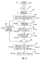
- the processing unit 18 provides the ALE signal (diamond 62) and the addressing code (rectangle 64) of the memory which is saved in time (T0 + 10ns) in the address register 16.
- the memory box is addressed or selected at time (T0 + 30ns) via the circuits of selection 12 (rectangle 68).
- the selected memory box is read at time (T0 + 50ns) (rectangle 70) and recording or writing binary signals read in the reading register 26 is performed at time (T0 + 60ns) (rectangle 72).
- the transfer (TRA signal) of the data from the reading 26 in the data register 28 takes place at the time (T0 + 70ns) in the presence of an ALE signal corresponding to a new address code that does not follow the preceding or an ADV signal indicating that the code address is the one following the previous one (rectangle 78).
- the data contained in the data register 28 is transmitted to the processing unit 18 by through the input / output circuit 20 to time (T0 + 90ns) which is controlled by the OE signal of the processing unit 18 (rectangle 80).
- next ALE signal and the following addressing code does not can only be taken into account at this time.
- the read register 26 is free for save the contents of a new memory cell, that is to say at time (T0 + 70ns).
- the signal ADV allows the incrementation (rectangle 82) of the address contained in the address register 16 of so that memory 10 is selected (rectangle 68) at time (T0 + 90ns), that reading (rectangle 70) takes place at the time (T0 + 110ns), that the writing (rectangle 72) in the reading register is performed at time (T0 + 120ns), that the transfer (rectangle 78) in the data register takes place at the time (T0 + 130ns) and that the output (rectangle 80) to the unit processing takes place on time (T0 + 150ns).
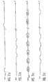
- the diagrams of figures 3-a to 3d are respectively time diagrams of ALE, ADV, ADD / DAT signals and OE, the ADD / DAT signal corresponding to either transfer of the ADD addressing code from the processing 18 to the address register 16, i.e. at transfer of the DAT data read from the data register 28 to processing unit 18, transfers taking place via the input / output circuit 20 and the bidirectional bus 46.
- the number 0, 1, 2, 3 or the letter J associated with the ADD address or the DAT data indicates that it is the address or the data of rank 0, 1, 2, 3, ... J.
- steps (C) and (H) of reading selected memory cells can understand, depending on the type of memory, a step in preload memory cells before reading real.
- the increment operation or step (e) can intervene as soon as the operation (c) is completed, that is to say as soon as the content of the reading register has been transferred to data register 28, which saves time and therefore increases the speed.
Landscapes
- Engineering & Computer Science (AREA)
- Microelectronics & Electronic Packaging (AREA)
- Read Only Memory (AREA)
- Bus Control (AREA)
Abstract
Description
- des moyens d'incrémentation pour augmenter d'au moins une unité le contenu du registre d'adresse de manière qu'il adresse les cellules de mémoire correspondant à l'adresse qui suit celle qu'il contient, et
- des moyens de mémorisation pour enregistrer le contenu du registre de lecture de manière qu'il puisse enregistrer les signaux lus dans les cellules de mémoire correspondant à l'adresse suivante.
- la figure 1 est un schéma fonctionnel d'un dispositif de lecture incrémentale d'une mémoire selon la présente invention,
- la figure 2 est un diagramme d'un cycle de lecture selon le procédé de l'invention, et
- les figures 3-a à 3-d sont des diagrammes temporels de signaux.
Claims (5)
- Dispositif de lecture incrémentale d'une mémoire (10) d'une unité centrale de traitement (18) d'un micro-ordinateur à laquelle sont associés des circuits d'adressage (12, 16) des cellules de ladite mémoire comprenant un registre d'adresse (16), et des circuits de lecture (14) des signaux lus dans les cellules de ladite mémoire sélectionnées par lesdits circuits d'adressage comprenant au moins un premier registre dit de lecture (26) dans lequel les signaux lus sont enregistrés sous forme binaire, caractérisé en ce qu'il comprend ;des moyens d'incrémentation (32) pour augmenter d'au moins une unité le contenu du registre d'adresse (16) de manière qu'il adresse les cellules de mémoire correspondant à l'adresse qui suit celle qu'il contient, etdes moyens de mémorisation pour enregistrer le contenu du premier registre de lecture (26) de manière qu'il puisse enregistrer les signaux lus dans les cellules de mémoire correspondant à l'adresse suivante.
- Dispositif selon la revendication 1, caractérisé en ce que les moyens d'incrémentation du contenu du registre d'adresse (16) comprennent un circuit de séquencement (32) qui est commandé par des signaux (ALE,ADV) fournis par l'unité centrale et qui fournit un signal (INC) d'incrémentation du registre d'adresse (16).
- Dispositif selon la revendication 1 ou 2, caractérisé en ce que les moyens de mémorisation pour enregistrer le contenu du registre de lecture (26) comprennent un registre de donnée (28) et des circuits électroniques de transfert (30) qui sont commandés par un signal (TRA) fourni par les moyens d'incrémentation (32) du registre d'adresse (16).
- Procédé de lecture incrémentale d'une mémoire (10) d'une unité centrale de traitement (18) d'un micro-ordinateur à laquelle sont associés des circuits d'adressage (12, 16) des cellules de ladite mémoire comprenant un registre d'adresse (16) et des circuits de lecture (14) des signaux lus dans les cellules de ladite mémoire (10) sélectionnées par lesdits circuits d'adressage comprenant un premier registre dit de lecture (26) dans lequel les signaux lus sont enregistrés sous forme binaire, caractérisé en ce qu'il comprend les étapes suivantes :(a) - Enregistrement par l'unité centrale de traitement (18) d'un code d'adressage dans le registre d'adresse (16) ;(b) - Lecture des cellules de la mémoire sélectionnées par le code d'adressage ;(c) - Enregistrement des signaux lus lors de l'étape (b) dans le registre de lecture (26) puis, dans un registre de donnée (28) ;(d) - Transfert du contenu du registre de donnée vers l'unité centrale de traitement (18) ;(e) - Incrémentation d'au moins une unité du contenu du registre d'adresse (16) pour obtenir un nouveau code d'adressage ;(f) - Lecture des cellules de mémoire sélectionnées par le nouveau code d'adressage obtenu par l'opération (d) ;(g) - Enregistrement des signaux lus lors de l'étape (f) dans le registre de lecture (26) puis dans le registre de donnée (28) ;(h) - Transfert du contenu du registre de donnée (28) vers l'unité centrale (18) de traitement si le code d'adressage suivant correspond à l'adresse résultant de l'étape (e), puis retour à l'étape (e) ; et(i) - Retour à l'étape (a) si le code d'adressage suivant ne correspond pas à l'adresse résultant de l'étape (e).
- Procédé de lecture selon la revendication 4, caractérisé en ce que l'étape (e) intervient entre les étapes (c) et (d).
Applications Claiming Priority (2)
| Application Number | Priority Date | Filing Date | Title |
|---|---|---|---|
| FR9615514A FR2757305B1 (fr) | 1996-12-17 | 1996-12-17 | Dispositif et procede de lecture incrementale d'une memoire |
| FR9615514 | 1996-12-17 |
Publications (2)
| Publication Number | Publication Date |
|---|---|
| EP0849739A1 true EP0849739A1 (fr) | 1998-06-24 |
| EP0849739B1 EP0849739B1 (fr) | 1999-10-20 |
Family
ID=9498766
Family Applications (1)
| Application Number | Title | Priority Date | Filing Date |
|---|---|---|---|
| EP97402806A Expired - Lifetime EP0849739B1 (fr) | 1996-12-17 | 1997-11-21 | Dispositif et procédé de lecture incrémentale d'une mémoire |
Country Status (4)
| Country | Link |
|---|---|
| US (1) | US6178490B1 (fr) |
| EP (1) | EP0849739B1 (fr) |
| DE (1) | DE69700648T2 (fr) |
| FR (1) | FR2757305B1 (fr) |
Cited By (2)
| Publication number | Priority date | Publication date | Assignee | Title |
|---|---|---|---|---|
| EP1017059A1 (fr) * | 1998-12-30 | 2000-07-05 | STMicroelectronics S.r.l. | Procédé de lecture d'une mémoire, en particulier une mémoire non-volatile |
| EP1184869A3 (fr) * | 2000-07-27 | 2003-02-05 | Sony Corporation | Dispositif et méthode d'emmagasinage de données |
Families Citing this family (2)
| Publication number | Priority date | Publication date | Assignee | Title |
|---|---|---|---|---|
| US20080162858A1 (en) * | 2007-01-03 | 2008-07-03 | Freescale Semiconductor, Inc. | Hardware-based memory initialization with software support |
| US8725975B2 (en) * | 2007-01-03 | 2014-05-13 | Freescale Semiconductor, Inc. | Progressive memory initialization with waitpoints |
Citations (2)
| Publication number | Priority date | Publication date | Assignee | Title |
|---|---|---|---|---|
| EP0262413A1 (fr) * | 1986-09-04 | 1988-04-06 | Fujitsu Limited | Dispositif de mémoire à multiplexage d'adresses |
| EP0333231A2 (fr) * | 1988-03-18 | 1989-09-20 | Nec Corporation | Système micro-ordinateur pouvant accéder à une mémoire à vitesse élevée |
Family Cites Families (5)
| Publication number | Priority date | Publication date | Assignee | Title |
|---|---|---|---|---|
| JPS59165300A (ja) * | 1983-03-10 | 1984-09-18 | Fujitsu Ltd | メモリ障害訂正方式 |
| US5093807A (en) * | 1987-12-23 | 1992-03-03 | Texas Instruments Incorporated | Video frame storage system |
| US5745791A (en) * | 1992-09-16 | 1998-04-28 | Intel Corporation | System for interfacing first and second components having different data path width by generating first and second component address to read data into buffer |
| US5465343A (en) * | 1993-04-30 | 1995-11-07 | Quantum Corporation | Shared memory array for data block and control program storage in disk drive |
| JPH10334659A (ja) * | 1997-05-29 | 1998-12-18 | Mitsubishi Electric Corp | 同期型半導体記憶装置 |
-
1996
- 1996-12-17 FR FR9615514A patent/FR2757305B1/fr not_active Expired - Fee Related
-
1997
- 1997-11-21 EP EP97402806A patent/EP0849739B1/fr not_active Expired - Lifetime
- 1997-11-21 DE DE69700648T patent/DE69700648T2/de not_active Expired - Fee Related
- 1997-12-16 US US08/991,428 patent/US6178490B1/en not_active Expired - Lifetime
Patent Citations (2)
| Publication number | Priority date | Publication date | Assignee | Title |
|---|---|---|---|---|
| EP0262413A1 (fr) * | 1986-09-04 | 1988-04-06 | Fujitsu Limited | Dispositif de mémoire à multiplexage d'adresses |
| EP0333231A2 (fr) * | 1988-03-18 | 1989-09-20 | Nec Corporation | Système micro-ordinateur pouvant accéder à une mémoire à vitesse élevée |
Cited By (3)
| Publication number | Priority date | Publication date | Assignee | Title |
|---|---|---|---|---|
| EP1017059A1 (fr) * | 1998-12-30 | 2000-07-05 | STMicroelectronics S.r.l. | Procédé de lecture d'une mémoire, en particulier une mémoire non-volatile |
| US6477625B1 (en) | 1998-12-30 | 2002-11-05 | Stmelectronics S.R.L. | Method and system for reading a memory by applying control signals thereto |
| EP1184869A3 (fr) * | 2000-07-27 | 2003-02-05 | Sony Corporation | Dispositif et méthode d'emmagasinage de données |
Also Published As
| Publication number | Publication date |
|---|---|
| FR2757305B1 (fr) | 1999-01-15 |
| US6178490B1 (en) | 2001-01-23 |
| EP0849739B1 (fr) | 1999-10-20 |
| DE69700648D1 (de) | 1999-11-25 |
| FR2757305A1 (fr) | 1998-06-19 |
| DE69700648T2 (de) | 2000-05-31 |
Similar Documents
| Publication | Publication Date | Title |
|---|---|---|
| EP1072024B1 (fr) | Procede de commutation d'applications sur une carte a puce multi-applicative | |
| EP0166838B1 (fr) | Procédé et dispositif pour détecter une configuration de bits particulière dans un train de bits en série | |
| EP0849739B1 (fr) | Dispositif et procédé de lecture incrémentale d'une mémoire | |
| EP0298002A1 (fr) | Mémoire de transposition pour circuit de traitement de données | |
| FR2533737A1 (fr) | Reseau de resolution de l'algorithme de l'element le moins recemment utilise | |
| FR2488420A1 (fr) | Dispositif d'obtention de l'histogramme des distances dans le temps entre des evenements successifs | |
| EP0849740B1 (fr) | Procédé et dispositif de lecture avec prédiction d'une mémoire | |
| EP0733977B1 (fr) | Système informatique avec mémoires hiérarchisées | |
| EP0823707A3 (fr) | Appareil à disque avec unité de traitement du signal | |
| EP0013853A1 (fr) | Dispositif de transfert de données entre une unité centrale d'un calculateur numérique et une unité périphérique | |
| EP1544724B1 (fr) | Nouvelle architecture de mémoire FIFO et procédé de gestion d'une telle mémoire | |
| EP1027642B1 (fr) | Microprocesseur comprenant des moyens de concatenation de bits | |
| SU1451723A2 (ru) | Устройство дл вычислени мультипликативной свертки | |
| EP0449190B1 (fr) | Programmateur produisant des signaux de sortie binaires en réponse à un signal de rythme | |
| EP0842465B1 (fr) | Systeme d'organisation et procede de sequencement des circuits d'un microprocesseur | |
| EP1235225A2 (fr) | Procédé et dispositif de lecture séquentielle d'une mémoire avec saut d'adresse | |
| EP0328436B1 (fr) | Procédé et dispositif de décodage partiel de l'entête d'un message de communication émis par une première station vers au moins une seconde station, notamment dans un véhicule automobile | |
| SU567174A1 (ru) | Устройство дл сжати информации | |
| EP0180680B1 (fr) | Circuit de comptage destiné en particulier à être associé à un capteur incrémental et apte à coopérer avec un calculateur à huit ou seize caractères binaires | |
| FR2539939A1 (fr) | Unite de commutation pour commutateur de donnees numeriques par paquets | |
| EP0595707B1 (fr) | Séquenceur linéaire avec signaux de sortie binaires | |
| SU1553985A1 (ru) | Коррел тор | |
| SU1246140A1 (ru) | Запоминающее устройство с коррекцией программы | |
| FR2643992A1 (fr) | Systeme de traitement des donnees, capable de memoriser des donnees de commande dans une memoire de commande avec une vitesse accrue | |
| KR910007512Y1 (ko) | 다중 입력 데이터 획득회로 |
Legal Events
| Date | Code | Title | Description |
|---|---|---|---|
| PUAI | Public reference made under article 153(3) epc to a published international application that has entered the european phase |
Free format text: ORIGINAL CODE: 0009012 |
|
| AK | Designated contracting states |
Kind code of ref document: A1 Designated state(s): DE FR GB IT |
|
| AX | Request for extension of the european patent |
Free format text: AL;LT;LV;MK;RO;SI |
|
| 17P | Request for examination filed |
Effective date: 19980720 |
|
| RAP3 | Party data changed (applicant data changed or rights of an application transferred) |
Owner name: STMICROELECTRONICS S.A. |
|
| GRAG | Despatch of communication of intention to grant |
Free format text: ORIGINAL CODE: EPIDOS AGRA |
|
| AKX | Designation fees paid |
Free format text: DE FR GB IT |
|
| RBV | Designated contracting states (corrected) |
Designated state(s): DE FR GB IT |
|
| 17Q | First examination report despatched |
Effective date: 19990303 |
|
| GRAG | Despatch of communication of intention to grant |
Free format text: ORIGINAL CODE: EPIDOS AGRA |
|
| GRAH | Despatch of communication of intention to grant a patent |
Free format text: ORIGINAL CODE: EPIDOS IGRA |
|
| GRAH | Despatch of communication of intention to grant a patent |
Free format text: ORIGINAL CODE: EPIDOS IGRA |
|
| GRAA | (expected) grant |
Free format text: ORIGINAL CODE: 0009210 |
|
| AK | Designated contracting states |
Kind code of ref document: B1 Designated state(s): DE FR GB IT |
|
| GBT | Gb: translation of ep patent filed (gb section 77(6)(a)/1977) |
Effective date: 19991014 |
|
| GBT | Gb: translation of ep patent filed (gb section 77(6)(a)/1977) |
Effective date: 19991021 |
|
| REF | Corresponds to: |
Ref document number: 69700648 Country of ref document: DE Date of ref document: 19991125 |
|
| ITF | It: translation for a ep patent filed | ||
| PLBE | No opposition filed within time limit |
Free format text: ORIGINAL CODE: 0009261 |
|
| STAA | Information on the status of an ep patent application or granted ep patent |
Free format text: STATUS: NO OPPOSITION FILED WITHIN TIME LIMIT |
|
| 26N | No opposition filed | ||
| REG | Reference to a national code |
Ref country code: GB Ref legal event code: IF02 |
|
| PGFP | Annual fee paid to national office [announced via postgrant information from national office to epo] |
Ref country code: DE Payment date: 20031204 Year of fee payment: 7 |
|
| PG25 | Lapsed in a contracting state [announced via postgrant information from national office to epo] |
Ref country code: DE Free format text: LAPSE BECAUSE OF NON-PAYMENT OF DUE FEES Effective date: 20050601 |
|
| PGFP | Annual fee paid to national office [announced via postgrant information from national office to epo] |
Ref country code: FR Payment date: 20051108 Year of fee payment: 9 |
|
| PGFP | Annual fee paid to national office [announced via postgrant information from national office to epo] |
Ref country code: GB Payment date: 20051116 Year of fee payment: 9 |
|
| PG25 | Lapsed in a contracting state [announced via postgrant information from national office to epo] |
Ref country code: IT Free format text: LAPSE BECAUSE OF NON-PAYMENT OF DUE FEES;WARNING: LAPSES OF ITALIAN PATENTS WITH EFFECTIVE DATE BEFORE 2007 MAY HAVE OCCURRED AT ANY TIME BEFORE 2007. THE CORRECT EFFECTIVE DATE MAY BE DIFFERENT FROM THE ONE RECORDED. Effective date: 20051121 |
|
| GBPC | Gb: european patent ceased through non-payment of renewal fee |
Effective date: 20061121 |
|
| REG | Reference to a national code |
Ref country code: FR Ref legal event code: ST Effective date: 20070731 |
|
| PG25 | Lapsed in a contracting state [announced via postgrant information from national office to epo] |
Ref country code: GB Free format text: LAPSE BECAUSE OF NON-PAYMENT OF DUE FEES Effective date: 20061121 |
|
| PG25 | Lapsed in a contracting state [announced via postgrant information from national office to epo] |
Ref country code: FR Free format text: LAPSE BECAUSE OF NON-PAYMENT OF DUE FEES Effective date: 20061130 |