EP0263277A2 - Flexible elektrische Verbindung und Verfahren zum Herstellen derselben - Google Patents
Flexible elektrische Verbindung und Verfahren zum Herstellen derselben Download PDFInfo
- Publication number
- EP0263277A2 EP0263277A2 EP87112150A EP87112150A EP0263277A2 EP 0263277 A2 EP0263277 A2 EP 0263277A2 EP 87112150 A EP87112150 A EP 87112150A EP 87112150 A EP87112150 A EP 87112150A EP 0263277 A2 EP0263277 A2 EP 0263277A2
- Authority
- EP
- European Patent Office
- Prior art keywords
- substrate
- electrical connection
- flexible electrical
- area
- relatively low
- Prior art date
- Legal status (The legal status is an assumption and is not a legal conclusion. Google has not performed a legal analysis and makes no representation as to the accuracy of the status listed.)
- Withdrawn
Links
Images


Classifications
-
- H—ELECTRICITY
- H05—ELECTRIC TECHNIQUES NOT OTHERWISE PROVIDED FOR
- H05K—PRINTED CIRCUITS; CASINGS OR CONSTRUCTIONAL DETAILS OF ELECTRIC APPARATUS; MANUFACTURE OF ASSEMBLAGES OF ELECTRICAL COMPONENTS
- H05K3/00—Apparatus or processes for manufacturing printed circuits
- H05K3/40—Forming printed elements for providing electric connections to or between printed circuits
- H05K3/4092—Integral conductive tabs, i.e. conductive parts partly detached from the substrate
-
- H—ELECTRICITY
- H05—ELECTRIC TECHNIQUES NOT OTHERWISE PROVIDED FOR
- H05K—PRINTED CIRCUITS; CASINGS OR CONSTRUCTIONAL DETAILS OF ELECTRIC APPARATUS; MANUFACTURE OF ASSEMBLAGES OF ELECTRICAL COMPONENTS
- H05K1/00—Printed circuits
- H05K1/02—Details
- H05K1/0271—Arrangements for reducing stress or warp in rigid printed circuit boards, e.g. caused by loads, vibrations or differences in thermal expansion
-
- H—ELECTRICITY
- H05—ELECTRIC TECHNIQUES NOT OTHERWISE PROVIDED FOR
- H05K—PRINTED CIRCUITS; CASINGS OR CONSTRUCTIONAL DETAILS OF ELECTRIC APPARATUS; MANUFACTURE OF ASSEMBLAGES OF ELECTRICAL COMPONENTS
- H05K3/00—Apparatus or processes for manufacturing printed circuits
- H05K3/30—Assembling printed circuits with electric components, e.g. with resistors
- H05K3/32—Assembling printed circuits with electric components, e.g. with resistors electrically connecting electric components or wires to printed circuits
- H05K3/34—Assembling printed circuits with electric components, e.g. with resistors electrically connecting electric components or wires to printed circuits by soldering
- H05K3/341—Surface mounted components
- H05K3/3431—Leadless components
- H05K3/3442—Leadless components having edge contacts, e.g. leadless chip capacitors, chip carriers
-
- H—ELECTRICITY
- H05—ELECTRIC TECHNIQUES NOT OTHERWISE PROVIDED FOR
- H05K—PRINTED CIRCUITS; CASINGS OR CONSTRUCTIONAL DETAILS OF ELECTRIC APPARATUS; MANUFACTURE OF ASSEMBLAGES OF ELECTRICAL COMPONENTS
- H05K2201/00—Indexing scheme relating to printed circuits covered by H05K1/00
- H05K2201/03—Conductive materials
- H05K2201/0332—Structure of the conductor
- H05K2201/0388—Other aspects of conductors
- H05K2201/0394—Conductor crossing over a hole in the substrate or a gap between two separate substrate parts
-
- H—ELECTRICITY
- H05—ELECTRIC TECHNIQUES NOT OTHERWISE PROVIDED FOR
- H05K—PRINTED CIRCUITS; CASINGS OR CONSTRUCTIONAL DETAILS OF ELECTRIC APPARATUS; MANUFACTURE OF ASSEMBLAGES OF ELECTRICAL COMPONENTS
- H05K2201/00—Indexing scheme relating to printed circuits covered by H05K1/00
- H05K2201/10—Details of components or other objects attached to or integrated in a printed circuit board
- H05K2201/10613—Details of electrical connections of non-printed components, e.g. special leads
- H05K2201/10621—Components characterised by their electrical contacts
- H05K2201/10727—Leadless chip carrier [LCC], e.g. chip-modules for cards
-
- H—ELECTRICITY
- H05—ELECTRIC TECHNIQUES NOT OTHERWISE PROVIDED FOR
- H05K—PRINTED CIRCUITS; CASINGS OR CONSTRUCTIONAL DETAILS OF ELECTRIC APPARATUS; MANUFACTURE OF ASSEMBLAGES OF ELECTRICAL COMPONENTS
- H05K2201/00—Indexing scheme relating to printed circuits covered by H05K1/00
- H05K2201/10—Details of components or other objects attached to or integrated in a printed circuit board
- H05K2201/10613—Details of electrical connections of non-printed components, e.g. special leads
- H05K2201/10742—Details of leads
- H05K2201/1075—Shape details
- H05K2201/10757—Bent leads
-
- Y—GENERAL TAGGING OF NEW TECHNOLOGICAL DEVELOPMENTS; GENERAL TAGGING OF CROSS-SECTIONAL TECHNOLOGIES SPANNING OVER SEVERAL SECTIONS OF THE IPC; TECHNICAL SUBJECTS COVERED BY FORMER USPC CROSS-REFERENCE ART COLLECTIONS [XRACs] AND DIGESTS
- Y02—TECHNOLOGIES OR APPLICATIONS FOR MITIGATION OR ADAPTATION AGAINST CLIMATE CHANGE
- Y02P—CLIMATE CHANGE MITIGATION TECHNOLOGIES IN THE PRODUCTION OR PROCESSING OF GOODS
- Y02P70/00—Climate change mitigation technologies in the production process for final industrial or consumer products
- Y02P70/50—Manufacturing or production processes characterised by the final manufactured product
Definitions
- the present invention generally relates to mounting an electronic device directly on a substrate when there is a mismatch between the thermal properties of the material making up the electronic device and the thermal properties of the material making up the substrate. More particularly, the present invention relates to mounting an electronic device, such as a semiconductor chip made primarily of silicon, directly on an organic substrate, such as printed circuit board made primarily of glass cloth impregnated with epoxy resin or other such material.
- an electronic circuit board may be constructed by soldering the leads (terminals) on electronic devices, such as semiconductor chips made primarily of silicon or semiconductor chip carriers (modules) made primarily of a ceramic material, to fixed conductive circuit lines on the surface of a printed circuit board made primarily of an organic material, such as glass cloth impregnated with epoxy resin or other such material, having a thermal coefficient of expansion which is significantly different from the thermal coefficient of expansion of the material(s) making up the electronic device.
- the object of the present invention is to provide a relatively simple stress relieving electrical connection for mounting an electronic device directly on a substrate when there is a mismatch between the thermal properties of the material(s) making up the electronic device and the material(s) making up the substrate; a further object of the present invention is to provide a method for making such stress relieving electrical connections.
- the invention as claimed attains these objects by providing flexible electrical connections as part of circuit lines on a substrate made of a material, such as glass cloth impregnated with epoxy resin, on which it is desired to mount an electronic device made of a material(s) having significantly different thermal properties, such as a semiconductor chip made primarily of silicon or a semiconductor chip carrier (module) made primarily of a ceramic material.
- Each flexible electrical connection comprises a terminus of one of the circuit lines having a stress relief bend floating on a relatively low adhesion area of the substrate where it is desired to connect the electronic device to the circuit lines on the substrate.
- Each flexible electrical connection provides relief of thermal and other such stresses which could damage or otherwise undesirably affect electrical circuit connections between the circuit line termini and leads (terminals) of the electronic device.
- Such a flexible electrical connection according to the present invention may be made by processing a selected surface portion of a substrate to form a relatively low adhesive area surrounded by a relatively high adhesive area. Then, a circuit line pattern may be formed on the substrate, including circuit lines having termini with stress relief bends located in the relatively low adhesive area on the surface of the substrate so that the terminus of each of these circuit lines floats on the surface of the substrate while the remainder of the circuit line is securely fixed to the relatively high adhesive area on the surface of the substrate.
- These floating termini of the circuit lines having the stress relief bends form the flexible electrical connections to which leads (terminals) of an electronic device may be joined by soldering, thermal compression bonding, ultrasonic bonding, or by using other such suitable bonding techniques.
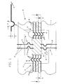
- a plan view is shown of a portion of a printed circuit board or card 10 made primarily of glass cloth impregnated with an epoxy resin, having a plurality of circuit lines 11 each having a terminus 16 located in a relatively low adhesion area 2 of the printed circuit board 10, which provides a flexible electrical connection for mounting a semiconductor chip 20 made primarily of silicon directly on the circuit board 10 according to the principles of the present invention.
- the area 2 of the printed circuit board 10 is somewhat larger than the size of the chip 20 which it is desired to mount on the circuit board 10. For example, if the semiconductor chip 20 is a six millimeter square device, then the area 2 may be an approximately fifteen millimeter square area. However, it should be noted that the chip 20 and the corresponding area 2 of the printed circuit board 10 may be selected to be virtually any practical size.
- Each of the circuit lines 11 is made of copper or other such suitable conductive material, and is sized to accommodate the semiconductor chip 20 which is connected to the circuit lines 11.
- each of the circuit lines 11 may have a width of approximately 7.6 to 12.7 microns (about 0.0003 to 0.0005 inch) and a height of approximately 12.7 to 35.6 microns (about 0.0005 to 0.0014 inch), with a spacing between the circuit lines 11 of approximately 25.4 to 152.4 microns (about 0.001 to 0.006 inch).
- the terminus 16 of each of the circuit lines 11 "floats" on the surface of the printed circuit board 10, and includes a stress relief bend 17, for relieving stresses, especially thermal stresses, which may affect the physical and electrical connection of the semiconductor chip 20 to the circuit lines 11 on the printed circuit board 10.
- the term "float” as used herein means that in the area 2 of the printed circuit board 10, the terminus 16 of each of the circuit lines 11 does not adhere sufficiently to the underlying surface of the circuit board 10 to fix the terminus 16 in place, but does adhere sufficiently to the underlying surface of the circuit board 10 to prevent gross movements of the terminus 16.
- the terminus 16 of each of the circuit lines 11 may move (float) on the surface of the circuit board 10 to relieve stress, without adversely affecting the overall electrical and physical characteristics of the circuit lines 11.
- portion 19 of each of the printed circuit lines 11 does adhere sufficiently to the underlying surface of the printed circuit board 10 to fix the portion 19 of each of the circuit lines 11 in place on the circuit board 10.
- the terminus 16 of each of the circuit lines 11 may adhere to the underlying circuit board 10 in the area 2 with a force of less than approximately 0.35 newton per linear millimeter (about two pounds per linear inch), while the portion 19 of each of the circuit lines 11 may adhere to the underlying circuit board 10 in the area 4 with a force of at least approximately 0.88 newton per linear millimeter (about five pounds per linear inch).
- This difference in adhesion between the terminus 16, and the portion 19, of each of the circuit lines 11, to the area 2 and the area 4, respectively, of the printed circuit board 10 is an important aspect of providing a relatively simple stress relieving electrical connection according to the principles of the present invention.
- the stress relief bend 17 of each of the circuit lines 11 is generally "U” shaped with the “U” having a height (A) of approximately two to three times the width (B) of the circuit line 11, and a width (C) of approximately four to six times the width (B) of the circuit line 11.
- the stress relief bend 17 is generally "U” shaped with the "U” having a height (A) of approximately 15.2 to 22.8 microns (about 0.0006 to 0.0009 inch) and a width (C) of approximately 30.4 to 45.6 microns (about 0.0012 to 0.0018 inch).
- each stress relief bend 17 of the terminus 16 of each of the circuit lines 11 may have any one of a number of sizes and configurations capable of relieving the undesired stresses, and, if desired for certain applications, each stress relief bend 17 may have a different size and configuration, as long as the sizes and configurations of the stress relief bends 17 are designed to provide a suitable overall pattern for the circuit lines 11.
- An especially desirable configuration for the stress relief bends 17 to maintain a desired circuit line density is a nested configuration with each of the adjacent circuit lines 11 running generally parallel to each other with adjacent stress relief bends 17 having a relatively low profile (that is, relatively unpronounced generally "U"-shaped curvature) and nested together.
- Figure 2 is a cross sectional view of the printed circuit board 10 with the semiconductor chip 20 mounted thereon taken along line I-I of Figure 1.
- the semiconductor chip 20 has electrical terminals (leads) 30 which are physically and electrically connected by solder columns 14 to the termini 16 of the circuit lines 11.
- each of these connections between the terminals 30 of the semiconductor chip 20 and the termini 16 of the circuit lines 11 may be a controlled collapse chip connection (C-4).
- C-4 controlled collapse chip connection
- the electrical terminals 30 of the semiconductor chip 10 may be connected to the termini 16 of the circuit lines 11 by wire bonding or by any other suitable technique.
- the printed circuit board 10 comprises a substrate 12 having a surface area 2 (also see Figure 1) to which the terminus 16 of each of the circuit lines 11 does not adhere sufficiently to fix the terminus 16 in place, and thus the terminus floats on this area 2 of the substrate 12 to provide stress relief as discussed previously.
- area 4 of the circuit board 10 also see Figure 1
- the portions 19 of the circuit lines 11 adhere sufficiently to the underlying substrate 12 to fix the circuit lines 11 in position on the circuit board 10.
- the substrate 12 of the printed circuit board 10 comprises primarily an organic material, such as glass cloth impregnated with epoxy resin (prepreg) or other such material.
- the substrate 12 may be made primarily of polyimide, a polyimide/glass composition, or any other such suitable circuit board material.
- Figures 1 and 2 show a semiconductor chip 20, preferably made primarily of silicon, mounted on the printed circuit board 10, other suitable electronic devices may be mounted on the circuit board 10 in accordance with the principles of the present invention.
- a resistor or capacitor having suitable electrical terminals may be mounted on the circuit board 10, or a ceramic module housing a semiconductor chip may be directly mounted on the printed circuit board 10, according to the principles of the present invention.
- the flexible electrical connection described above is made as described below referring to Figures 3 and 4 of the drawing.
- Figures 3 and 4 are cross sectional views, each taken along the line II-II of Figure 1, schematically illustrating certain steps in this preferred method for making a flexible electrical connection in accordance with the principles of the present invention.
- a typical substrate 12 may be a structure in the shape of a rectangular board having a thickness of approximately 1,026 to 1,538 microns (0.040 to 0.060 inch), which is made by laminating together several layers of glass cloth impregnated with epoxy resin.
- the layer of material 15 may be, for example, an approximately 5.1 microns (about 0.0002 inch) thick layer of copper.
- Such a copper layer 15 may be placed on such an organic substrate 12 using any suitable process.
- a sheet of "peel apart copper” on a suitable carrier such as copper
- a release layer between the peel apart copper and the carrier may be brought into contact with the surface of the substrate 12.
- the carrier and the release layer may be removed from the sheet of peel apart copper which adheres to the underlying organic substrate 12 and remains in place as the copper layer 15 on the organic substrate 12.
- a "peel apart copper” product is commercially available from Yates, Inc. having a place of business in Bordentown, New Jersey.
- Figure 3 shows in cross section the organic substrate 12 having the copper layer 15 thereon with the photoresist material 21 exposed and developed to form the desired image in the relatively low adhesion area 2.
- the portions of the copper layer 15 not covered by the photoresist material 21 are removed, for example, by using any suitable conventional copper etching process, to leave the copper layer 15 only in those areas protected by the photoresist material 21. Then, the photoresist material 21 is removed, for example, by using a suitable conventional photoresist stripping process.
- a cationic surfactant such as Reten 210 which is commercially available from Hercules Powder Company having a place of business in Wilmington, Delaware, is applied to the entire surface of the substrate 12, including the area 2 of the substrate 12 having the copper layer 15 with the pattern of the terminus 16 and the stress relief bend 17 of each of the circuit lines 11 which it is desired to form on the substrate 12.
- This application of the cationic surfactant is followed by a seeding of the entire surface of the substrate 12 with a colloidal tin/palladium seed layer, for example, such as described in United States Patent 4,448,804 which is assigned to International Business Machines (IBM) Corporation and which is incorporated herein by reference.
- Another (second) layer of photoresist (not shown), such as Riston type T168 photoresist which is commercially available from E.I. Du Pont de Nemours and Company having a place of business in Wilmington, Delaware, is applied over the entire surface of the substrate 12.
- This second layer of photoresist material is exposed and developed using conventional photoresist processing techniques to form a negative image of the entire circuit line pattern which it is desired to construct on the substrate 12. More specifically, this second layer of photoresist material is exposed and developed to form a negative image corresponding to all of the circuit lines 11 which it is desired to form on the substrate 12 of the circuit board 10, including the termini 16 having the stress relief bends 17 in the area 2, and the portions 19 in the area 4, of the circuit lines 11.
- the circuit lines 11 are formed by depositing a conductive material, preferably copper, onto the areas of the substrate 12 not covered by the photoresist, including those areas of the substrate 12 with the copper layer 15 which was left on the substrate 12 after the first photoresist process described above and which is patterned with the configuration of the terminus 16 with the stress relief bend 17 of each of the circuit lines 11.
- the conductive material may be deposited on the substrate 12 in any suitable manner to form the circuit lines 11.
- copper may be deposited on the substrate 12 to form the circuit lines 11 by using a conventional additive copper plating process.
- the photoresist forming the negative image of the desired circuit lines 11 is then removed, for example, by using a suitable conventional photoresist stripping process to leave the structure shown in Figure 4.
- each of the circuit lines 11 having a terminus 16 with a stress relief bend 17 floating on a relatively low adhesion area 2 of the substrate 12 of the circuit board 10, and having a portion 19 fixed on a relatively high adhesion area 4 of the substrate 12 of the circuit board 10.
- the terminus 16 with the stress relief bend 17 of each of the circuit lines 11 floats on the area 2 of the substrate 12 of the circuit board 10 due to the above described treatment of the underlying copper layer 15 with the cationic surfactant. This treatment dramatically decreases the adhesion of the terminus 16 with the stress relief bend 17 of each of the circuit lines 11 to the underlying copper layer 15 on the substrate 12 of the circuit board 10, relative to the adhesion which would otherwise occur.
- this treatment reduces copper to copper adhesion from approximately 2.64 newtons per linear millimeter (about fifteen pounds per linear inch) to approximately 0.18 to 0.35 newtons per linear millimeter (about one to two pounds per linear inch).
- this treatment dramatically increases the adhesion of the portion 19 of each of the circuit lines 11 to the substrate 12 of the circuit board 10 in the area 4 since the copper layer 15 is not present in this area 4 and the cationic surfactant followed by the seeding with the colloidal tin/palladium acts to increase the adhesion in this area 4, relative to the adhesion which would otherwise occur.
- this treatment increases copper to glass cloth/epoxy resin adhesion from approximately 0.35 to 0.53 newtons per linear millimeter (about two to three pounds per linear inch) to approximately 0.70 to 0.88 newtons per linear millimeter (about four to five pounds per linear inch).
- the foregoing preferred method according to the present invention results in each of the circuit lines 11 having a terminus 16 with a stress relief bend 17 floating on a relatively low adhesion area 2 of the substrate 12 of the circuit board 10 to provide a relatively simple stress relieving electrical connection which may be used for mounting an electronic device directly on the circuit board 10, as described previously.
- the relatively low adhesive area 2 on the substrate 12 of the circuit board 10 may be followed except that, prior to applying the first photoresist material 21, the entire copper layer 15 placed on the substrate 12 is etched away from the substrate 12 and then the photoresist material 21 is applied, exposed and developed to protect only the area 4 and to not cover any of the area 2 of the circuit board 10.
- the open area 2 is treated with concentrated sulfuric acid, or vapor blasted, after which the remaining steps of the foregoing method are followed.
- the sulfuric acid or vapor blast treatment of the open area 2 results in reducing the adhesion of the circuit lines 11 to this area 2 of the substrate 12 of the circuit board 10, relative to the adhesion which would otherwise occur.
- the foregoing method may be followed except that the copper layer 15 is selectively pretreated with sulfuric acid, vapor blast or etching, prior to bringing the copper layer 15 into contact with the surface of the substrate 12 and laminating the copper layer 15 to the substrate 12 with the selectively pretreated side of the copper layer 15 facing the surface of the substrate 12.
- This selective pretreatment will generate smooth areas on the copper layer 15 which, upon lamination and subsequent complete removal of the copper 15, will cause smooth areas to form on the surface of the substrate 12 which replicate the smooth areas on the copper layer 15 which are selected to have the pattern of the terminus 16 of each of circuit lines 11 which it is desired to form on the relatively low adhesion area 2 of the substrate 12 of the circuit board 10.
- This selective smoothing in the area 2 of the circuit board 10 reduces the adhesion of the circuit lines 11 to this area 2 of the substrate 12 of the circuit board 10, relative to the adhesion which would otherwise occur.
Landscapes
- Engineering & Computer Science (AREA)
- Microelectronics & Electronic Packaging (AREA)
- Manufacturing & Machinery (AREA)
- Structure Of Printed Boards (AREA)
- Wire Bonding (AREA)
- Combinations Of Printed Boards (AREA)
Applications Claiming Priority (2)
| Application Number | Priority Date | Filing Date | Title |
|---|---|---|---|
| US06/915,485 US4728751A (en) | 1986-10-06 | 1986-10-06 | Flexible electrical connection and method of making same |
| US915485 | 1986-10-06 |
Publications (2)
| Publication Number | Publication Date |
|---|---|
| EP0263277A2 true EP0263277A2 (de) | 1988-04-13 |
| EP0263277A3 EP0263277A3 (de) | 1989-03-15 |
Family
ID=25435830
Family Applications (1)
| Application Number | Title | Priority Date | Filing Date |
|---|---|---|---|
| EP87112150A Withdrawn EP0263277A3 (de) | 1986-10-06 | 1987-08-21 | Flexible elektrische Verbindung und Verfahren zum Herstellen derselben |
Country Status (3)
| Country | Link |
|---|---|
| US (1) | US4728751A (de) |
| EP (1) | EP0263277A3 (de) |
| JP (1) | JPS6396934A (de) |
Cited By (3)
| Publication number | Priority date | Publication date | Assignee | Title |
|---|---|---|---|---|
| DE3835942A1 (de) * | 1988-10-21 | 1990-04-26 | Telefunken Electronic Gmbh | Flaechenhafter strahler |
| EP0355965A3 (de) * | 1988-08-16 | 1991-08-07 | DELCO ELECTRONICS CORPORATION (a Delaware corp.) | Verfahren zum Erreichen einer selektiven Adhäsionshemmung und -steuerung in Dickschicht-Leitern |
| US5122929A (en) * | 1988-08-16 | 1992-06-16 | Delco Electronics Corporation | Method of achieving selective inhibition and control of adhesion in thick-film conductors |
Families Citing this family (40)
| Publication number | Priority date | Publication date | Assignee | Title |
|---|---|---|---|---|
| US5476211A (en) * | 1993-11-16 | 1995-12-19 | Form Factor, Inc. | Method of manufacturing electrical contacts, using a sacrificial member |
| US5917707A (en) * | 1993-11-16 | 1999-06-29 | Formfactor, Inc. | Flexible contact structure with an electrically conductive shell |
| GB8706610D0 (en) * | 1987-03-19 | 1987-04-23 | Smith Ind Plc | Electrical components |
| US4851613A (en) * | 1988-06-08 | 1989-07-25 | Flex Technology, Inc. | Flexible circuit laminate for surface mount devices |
| US4959751A (en) * | 1988-08-16 | 1990-09-25 | Delco Electronics Corporation | Ceramic hybrid integrated circuit having surface mount device solder stress reduction |
| US5176853A (en) * | 1988-08-16 | 1993-01-05 | Delco Electronics Corporation | Controlled adhesion conductor |
| US5121298A (en) * | 1988-08-16 | 1992-06-09 | Delco Electronics Corporation | Controlled adhesion conductor |
| US5238702A (en) * | 1988-10-27 | 1993-08-24 | Henning Giesecke | Electrically conductive patterns |
| DE3932017A1 (de) * | 1988-10-27 | 1990-05-03 | Bayer Ag | Elektrisch leitende strukturen |
| US5283712A (en) * | 1988-10-27 | 1994-02-01 | Mazda Motor Corporation | Integrated circuit for vehicle |
| FR2646559B1 (fr) * | 1989-04-28 | 1991-07-05 | Commissariat Energie Atomique | Systeme de mesure constitue d'un circuit de detection d'un rayonnement, d'un circuit de lecture et d'un support tel qu'un doigt froid de cryostat |
| JPH03124010A (ja) * | 1989-10-08 | 1991-05-27 | Murata Mfg Co Ltd | 電子部品の端子 |
| WO1991013533A1 (en) * | 1990-03-01 | 1991-09-05 | Motorola, Inc. | Selectively releasing conductive runner and substrate assembly |
| US7198969B1 (en) | 1990-09-24 | 2007-04-03 | Tessera, Inc. | Semiconductor chip assemblies, methods of making same and components for same |
| US5166774A (en) * | 1990-10-05 | 1992-11-24 | Motorola, Inc. | Selectively releasing conductive runner and substrate assembly having non-planar areas |
| US5338391A (en) * | 1993-10-12 | 1994-08-16 | Motorola, Inc. | Method of making a substrate having selectively releasing conductive runners |
| US7200930B2 (en) * | 1994-11-15 | 2007-04-10 | Formfactor, Inc. | Probe for semiconductor devices |
| US7084656B1 (en) | 1993-11-16 | 2006-08-01 | Formfactor, Inc. | Probe for semiconductor devices |
| US5719749A (en) * | 1994-09-26 | 1998-02-17 | Sheldahl, Inc. | Printed circuit assembly with fine pitch flexible printed circuit overlay mounted to printed circuit board |
| US6313402B1 (en) | 1997-10-29 | 2001-11-06 | Packard Hughes Interconnect Company | Stress relief bend useful in an integrated circuit redistribution patch |
| JP2003014819A (ja) * | 2001-07-03 | 2003-01-15 | Matsushita Electric Ind Co Ltd | 半導体配線基板,半導体デバイス,半導体デバイスのテスト方法及びその実装方法 |
| US20040105244A1 (en) * | 2002-08-06 | 2004-06-03 | Ilyas Mohammed | Lead assemblies with offset portions and microelectronic assemblies with leads having offset portions |
| US7629691B2 (en) * | 2004-06-16 | 2009-12-08 | Honeywell International Inc. | Conductor geometry for electronic circuits fabricated on flexible substrates |
| DE102004050177A1 (de) * | 2004-10-14 | 2006-04-20 | Infineon Technologies Ag | Umverdrahtungsanlage eines Materialschnittstellen aufweisenden elektronischen Bauelements und Verfahren zu seiner Herstellung |
| US7462035B2 (en) | 2005-07-27 | 2008-12-09 | Physical Optics Corporation | Electrical connector configured as a fastening element |
| ATE500568T1 (de) * | 2005-11-28 | 2011-03-15 | Nxp Bv | Vorrichtung umfassend ein substrat mit einem elektrischen kontakt und transponder |
| WO2008021374A2 (en) | 2006-08-15 | 2008-02-21 | General Dynamics Advanced Information Systems, Inc | Methods for two-dimensional autofocus in high resolution radar systems |
| US8196291B2 (en) * | 2006-11-06 | 2012-06-12 | General Dynamics Advanced Information Systems, Inc. | Method for manufacturing leads |
| US7957100B1 (en) | 2007-08-29 | 2011-06-07 | Magnecomp Corporation | Disk drive gimbal having reduced residual stress and related method of manufacture |
| US8308489B2 (en) * | 2008-10-27 | 2012-11-13 | Physical Optics Corporation | Electrical garment and electrical garment and article assemblies |
| US8063307B2 (en) | 2008-11-17 | 2011-11-22 | Physical Optics Corporation | Self-healing electrical communication paths |
| US8883287B2 (en) * | 2009-06-29 | 2014-11-11 | Infinite Corridor Technology, Llc | Structured material substrates for flexible, stretchable electronics |
| US9385095B2 (en) | 2010-02-26 | 2016-07-05 | Taiwan Semiconductor Manufacturing Company, Ltd. | 3D semiconductor package interposer with die cavity |
| US9935090B2 (en) | 2014-02-14 | 2018-04-03 | Taiwan Semiconductor Manufacturing Company, Ltd. | Substrate design for semiconductor packages and method of forming same |
| US10056267B2 (en) | 2014-02-14 | 2018-08-21 | Taiwan Semiconductor Manufacturing Company, Ltd. | Substrate design for semiconductor packages and method of forming same |
| US10026671B2 (en) | 2014-02-14 | 2018-07-17 | Taiwan Semiconductor Manufacturing Company, Ltd. | Substrate design for semiconductor packages and method of forming same |
| US9653443B2 (en) | 2014-02-14 | 2017-05-16 | Taiwan Semiconductor Manufacturing Company, Ltd. | Thermal performance structure for semiconductor packages and method of forming same |
| US9564416B2 (en) | 2015-02-13 | 2017-02-07 | Taiwan Semiconductor Manufacturing Company, Ltd. | Package structures and methods of forming the same |
| TWI646877B (zh) | 2018-03-12 | 2019-01-01 | Chipbond Technology Corporation | 軟性電路基板之佈線結構 |
| JP2024538498A (ja) | 2021-09-07 | 2024-10-23 | ルミレッズ リミテッド ライアビリティ カンパニー | 屈曲ワイヤを有するled照明ストリップ |
Family Cites Families (12)
| Publication number | Priority date | Publication date | Assignee | Title |
|---|---|---|---|---|
| US3129280A (en) * | 1960-09-19 | 1964-04-14 | Amphenol Borg Electronics Corp | Electronic circuit boards with weldable terminals |
| US3248779A (en) * | 1963-11-15 | 1966-05-03 | Leonard J Yuska | Method of making an electronic module |
| DE1539692A1 (de) * | 1966-06-23 | 1969-10-16 | Blume & Redecker Gmbh | Umklebevorrichtung fuer Spulen |
| US3519890A (en) * | 1968-04-01 | 1970-07-07 | North American Rockwell | Low stress lead |
| US4048438A (en) * | 1974-10-23 | 1977-09-13 | Amp Incorporated | Conductor patterned substrate providing stress release during direct attachment of integrated circuit chips |
| US4026011A (en) * | 1975-08-28 | 1977-05-31 | Burroughs Corporation | Flexible circuit assembly |
| US4026759A (en) * | 1975-12-11 | 1977-05-31 | International Business Machines Corporation | Method of making ingrown lead frame with strain relief |
| US4295184A (en) * | 1978-08-21 | 1981-10-13 | Advanced Circuit Technology | Circuit board with self-locking terminals |
| FR2479639A1 (fr) * | 1980-03-25 | 1981-10-02 | Thomson Csf | Dispositif d'assemblage entre composants electroniques de caracteristiques mecaniques differentes et son procede de realisation |
| FR2486755A1 (fr) * | 1980-07-11 | 1982-01-15 | Socapex | Support de composants electroniques pour circuits hybrides de grandes dimensions |
| US4413308A (en) * | 1981-08-31 | 1983-11-01 | Bell Telephone Laboratories, Incorporated | Printed wiring board construction |
| US4448804A (en) * | 1983-10-11 | 1984-05-15 | International Business Machines Corporation | Method for selective electroless plating of copper onto a non-conductive substrate surface |
-
1986
- 1986-10-06 US US06/915,485 patent/US4728751A/en not_active Expired - Fee Related
-
1987
- 1987-05-25 JP JP62126102A patent/JPS6396934A/ja active Granted
- 1987-08-21 EP EP87112150A patent/EP0263277A3/de not_active Withdrawn
Cited By (4)
| Publication number | Priority date | Publication date | Assignee | Title |
|---|---|---|---|---|
| EP0355965A3 (de) * | 1988-08-16 | 1991-08-07 | DELCO ELECTRONICS CORPORATION (a Delaware corp.) | Verfahren zum Erreichen einer selektiven Adhäsionshemmung und -steuerung in Dickschicht-Leitern |
| US5122929A (en) * | 1988-08-16 | 1992-06-16 | Delco Electronics Corporation | Method of achieving selective inhibition and control of adhesion in thick-film conductors |
| DE3835942A1 (de) * | 1988-10-21 | 1990-04-26 | Telefunken Electronic Gmbh | Flaechenhafter strahler |
| US5084804A (en) * | 1988-10-21 | 1992-01-28 | Telefunken Electronic Gmbh | Wide-area lamp |
Also Published As
| Publication number | Publication date |
|---|---|
| EP0263277A3 (de) | 1989-03-15 |
| US4728751A (en) | 1988-03-01 |
| JPS6396934A (ja) | 1988-04-27 |
| JPH031831B2 (de) | 1991-01-11 |
Similar Documents
| Publication | Publication Date | Title |
|---|---|---|
| US4728751A (en) | Flexible electrical connection and method of making same | |
| US4873123A (en) | Flexible electrical connection and method of making same | |
| US6313402B1 (en) | Stress relief bend useful in an integrated circuit redistribution patch | |
| EP0277606B1 (de) | Elektronische Packungsstruktur | |
| US4048438A (en) | Conductor patterned substrate providing stress release during direct attachment of integrated circuit chips | |
| US5280139A (en) | Selectively releasing conductive runner and substrate assembly | |
| EP0013562B1 (de) | Verfahren zum Herstellen elektronischer Verkapselungen | |
| US5515604A (en) | Methods for making high-density/long-via laminated connectors | |
| US5798050A (en) | Process for fabrication of a selectively filled flexible adhesive device for solderless connection of electronic modules to a substrate | |
| EP0232533A2 (de) | Verfahren zum Herstellen eines integrierten Schaltungsproduktes mit einer Polyimidfilm-Verbindungsstruktur | |
| US20060101640A1 (en) | Method of fabricating rigid-flexible printed circuit board | |
| KR100399379B1 (ko) | 반도체 장치와 그의 제조 방법, 액정 모듈 및 그의 탑재방법 | |
| KR0157060B1 (ko) | 실장기판 | |
| US3010863A (en) | Method of manufacturing electrically insulating panels having a conductive pattern and panel manufactured by such method | |
| US5109601A (en) | Method of marking a thin film package | |
| EP0843357B1 (de) | Herstellungsverfahren einer Kontaktgitter-Halbleiterpackung | |
| US7045393B2 (en) | Method for manufacturing circuit devices | |
| JPH0529537A (ja) | 半導体モジユール構造 | |
| US4965700A (en) | Thin film package for mixed bonding of chips | |
| EP0095306B1 (de) | Verbindungsträger mit biegsamen Packungen | |
| US5926379A (en) | Electronic card assembly by means of solder connections | |
| EP0422828B1 (de) | Folienträger | |
| GB2276977A (en) | Reducing thermal stress in I.C. chip mountings | |
| EP0343379A2 (de) | Dünnschichtpackung für eine gemischte Chipverbindung | |
| JPH0831973A (ja) | フリップチップic実装方法及び半導体装置 |
Legal Events
| Date | Code | Title | Description |
|---|---|---|---|
| PUAI | Public reference made under article 153(3) epc to a published international application that has entered the european phase |
Free format text: ORIGINAL CODE: 0009012 |
|
| AK | Designated contracting states |
Kind code of ref document: A2 Designated state(s): DE FR GB |
|
| 17P | Request for examination filed |
Effective date: 19880823 |
|
| PUAL | Search report despatched |
Free format text: ORIGINAL CODE: 0009013 |
|
| AK | Designated contracting states |
Kind code of ref document: A3 Designated state(s): DE FR GB |
|
| 17Q | First examination report despatched |
Effective date: 19910411 |
|
| STAA | Information on the status of an ep patent application or granted ep patent |
Free format text: STATUS: THE APPLICATION IS DEEMED TO BE WITHDRAWN |
|
| 18D | Application deemed to be withdrawn |
Effective date: 19930302 |
|
| RIN1 | Information on inventor provided before grant (corrected) |
Inventor name: CANESTARO, MICHAEL JAMES Inventor name: SUMMA, WILLIAM JOSEPH |