EP0265285A2 - Elektromagnetische Abschirmung für gedrucke Leiterplatte - Google Patents
Elektromagnetische Abschirmung für gedrucke Leiterplatte Download PDFInfo
- Publication number
- EP0265285A2 EP0265285A2 EP87309401A EP87309401A EP0265285A2 EP 0265285 A2 EP0265285 A2 EP 0265285A2 EP 87309401 A EP87309401 A EP 87309401A EP 87309401 A EP87309401 A EP 87309401A EP 0265285 A2 EP0265285 A2 EP 0265285A2
- Authority
- EP
- European Patent Office
- Prior art keywords
- strip
- electromagnetic shield
- component
- pins
- walls
- Prior art date
- Legal status (The legal status is an assumption and is not a legal conclusion. Google has not performed a legal analysis and makes no representation as to the accuracy of the status listed.)
- Withdrawn
Links
Images

Classifications
-
- H—ELECTRICITY
- H05—ELECTRIC TECHNIQUES NOT OTHERWISE PROVIDED FOR
- H05K—PRINTED CIRCUITS; CASINGS OR CONSTRUCTIONAL DETAILS OF ELECTRIC APPARATUS; MANUFACTURE OF ASSEMBLAGES OF ELECTRICAL COMPONENTS
- H05K9/00—Screening of apparatus or components against electric or magnetic fields
- H05K9/0007—Casings
- H05K9/002—Casings with localised screening
- H05K9/0022—Casings with localised screening of components mounted on printed circuit boards [PCB]
- H05K9/0024—Shield cases mounted on a PCB, e.g. cans or caps or conformal shields
- H05K9/0032—Shield cases mounted on a PCB, e.g. cans or caps or conformal shields having multiple parts, e.g. frames mating with lids
-
- Y—GENERAL TAGGING OF NEW TECHNOLOGICAL DEVELOPMENTS; GENERAL TAGGING OF CROSS-SECTIONAL TECHNOLOGIES SPANNING OVER SEVERAL SECTIONS OF THE IPC; TECHNICAL SUBJECTS COVERED BY FORMER USPC CROSS-REFERENCE ART COLLECTIONS [XRACs] AND DIGESTS
- Y10—TECHNICAL SUBJECTS COVERED BY FORMER USPC
- Y10S—TECHNICAL SUBJECTS COVERED BY FORMER USPC CROSS-REFERENCE ART COLLECTIONS [XRACs] AND DIGESTS
- Y10S174/00—Electricity: conductors and insulators
- Y10S174/35—Box or housing mounted on substrate or PCB
Definitions
- the present invention relates to an electromagnetic shield, a component of an electromagnetic shield and a method of assembling an electromagnetic shield.
- the present invention relates to shielding devices for minimizing electromagnetic interference and susceptibility effects on electrical and electronic devices, and more particularly, to a shielding device that is easily formed to a desired size and shape, and to a method of assembly of the shielding device.
- shielding for electronic components found in radio transmitters, radio receivers, computers and other electronic devices that use circuitry susceptible to electromagnetic radiation. It is known that these components can be shielded from undesirable electromagnetic interference and its susceptibility effects with the use of a conductive shield that reflects or dissipates the electromagnetic charges and fields. Such shielding is generally grounded to allow the offending electrical charges and fields to be dissipated without disrupting the operation of the electronic components enclosed within the shield.
- a variety of known prior art shielding devices for components provided on printed circuit boards are frequently included within the same frame or packaging that supports the component being shielded.
- the shields are sometimes arranged close to the components being shielded. This close arrangement impedes effective ventilation of these components.
- a known shielding device is disclosed in U.S. Patent No. 4,433,886 issued on February 28, 1984 to Cassarly et al.
- the Cassarly et al. patent discloses a connector mounting for integrated circuit chip packages that includes a rectangularly shaped electromagnetic shield that is made from electrically conductive sheet metal.
- the shield has four uninterrupted side walls, from which extend a plurality of rigid ground contact pins.
- the shield also includes a snap-on cover member having a saddle-like frame that is hingedly mounted at one end to the connector mounting.
- the disclosed shield is preformed in specific shapes and sizes, and does not offer an end user the ability to adjust the shape or size of the shield.
- Such prior art shielding devices are generally manufactured in only one or a few different specific sizes that cannot be altered easily by the user. Therefore, if a wide variety of differently sized shields are desired, suppliers and users must maintain in stock a relatively large supply of such electromagnetic shields in many different shapes and sizes.
- an electromagnetic shield comprising: four electrically conductive walls arranged to form a rectangular frame; means projecting from a lower edge of the walls for engaging with a printed circuit board; deflectable engagement prongs extending from an upper edge of the walls; and an electrically conductive cover plate having width and length dimensions similar to those of the rectangular frame engaged within said engagement prongs; wherein the walls and engagement prongs are outwardly deflectable to allow for insertion and removal of the cover plate.
- the present invention also provides a component of an electromagnetic shield, comprising: a strip of electrically conductive metal; means projection from a first edge of the strip for engaging with a printed circuit board, said means projecting substantially perpendicular to a centre line of the strip; and a plurality of engagement prongs defined by a plurality of slots extending through a second edge of the strip in a direction substantially perpendicular to the center line of the strip.
- the present invention provides a method of assembling an electromagnetic shield, comprising the steps of: providing a strip of electrically conductive metal having pins extending from one edge thereof and engagement prongs extending from an opposite edge thereof; cutting the strip into a preferred length; forming the strip into a rectangle; and inserting the pins into holes in a printed circuit board.
- the wall of the shield may be made from a longitudinally extending strip of electrically conductive metal having longitudinally extending parallel edges and first and second ends.
- a plurality of pins extends substantially perpendicularly from one edge thereof and a plurality of engagement prongs extends from the other edge thereof.
- the engagement prongs may be adapted to retain a metal cover plate on the shield.
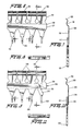
- a first preferred embodiment of an electromagnetic shield 10 is arranged on a printed circuit board 12 having a uniform grid of perforations.
- the electromagnetic shield 10 is designed to encompass and shield one or more electronic components (not shown) that are mounted on the printed circuit board 12.
- the electromagnetic shield 10 can be used to shield either a section of a printed circuit board or the entire board.
- the shield 10 includes a cover plate 14 and walls 16.
- the wall 16 are made from a single length or strip 18 of metallic material.
- the strip is stamped from 0.005" thick beryllium copper.
- other methods of forming may be used, and other materials including other metals and other alloys of copper may be used.
- the material be metals that are capable of being readily soldered or welded and be capable of low resistance electrical conductivity.
- the shield if the primary purpose of the shield is to protect against magnetic fields, it may be preferable to use a steel or steel alloy which has a relatively high permeability at low frequencies. To provide electrical conductivity at relatively low resistance, the steel may be plated with tin. If the principal concern is protection against electrical fields, then it may be preferable to use a copper alloy as will be readily apparent to one skilled in the art of electromagnetic shielding upon reading the present specification.
- the walls 16 could be formed into any reasonable configuration. However, in the preferred embodiment, the walls 16 are formed into a square or rectangle. By using the walls 16 in the form of a rectangle, the configuration of the cover plate 14 is simplified along with a simplification of mounting the walls 16 on a conventional printed circuit board 12.
- the strip material 18 has a plurality of pins 20 projecting from one edge thereof.
- the pins 20 extend about 0.125" from the edge of the strip material 18.
- the pins 20 are preferably equally spaced, and arranged for alignment with the holes in the printed circuit board 12 which are typically spaced 0.10" apart.
- the centers of the pins 20 would preferably be spaced 0.20" apart.
- the pins 20 have a three dimensional shape for additional stability.
- the pins 20 are U-shaped in cross section, with a radius of about 0.010".
- Small notches 22, preferably about .007" wide and .005" deep, may be formed in the pins 20 at the regions where the pins 20 join the strip material 18. With reference to Fig. 4, the notches 22 facilitate the bending of the pins 20 into a U-shaped cross section by separating the portions of the pins 20 that extend beyond the plane of the strip material 18 from the strip material 18.
- the embossment having a U-shaped cross section extends into regions 24 of the strip 18 that are adjacent to and in alignment with the pins 20.
- Each region 24 is preferably about 0.15" in length and appears as an extension of a pin 20. The effect of the regions 24 is to reduce the deflection of the walls 16 when the cover plate 14 is being attached to or removed from the shield 10.
- the strip material 18 has a plurality of engagement prongs 26 projecting from an edge opposite the edge from which the pins 20 project.
- the edge from which the engagement prongs 26 project is substantially parallel to the edge from which the pins 20 project.
- the regions 24 provide enough stiffness to support the prongs 26 without relying on adjoining sections of the walls 16 or corners.
- the prongs 26 each have a flanged end 28, preferably about 0.030" in length, to allow for easy insertion of the cover plate 14, and an outward curvature forming a recess 30 to receive and hold the cover plate 14.
- the recess 30 has a radius of about 0.025".
- the engagement prongs 26 are defined by uniformly spaced slots 32 formed along the edge of the strip material 18, the slots 32 extending perpendicular to the longitudinal direc tion of the strip material 18.
- Each slot 32 is preferably 0.030" wide, 0.215" in length, and 0.200" apart on centers. The spacing, width, and length of the slots 32 determine the dimensions of the prongs 26, which affects the deflectability of the prongs 26.
- the slots 32 allow the prongs 26 to work independently of each other to provide individual and continuous contact with the cover plate 14, even if the cover plate 14 is irregular or out of square.
- the slots 32 also provide ventilation to the shield 10.
- Circular openings 34 are provided at the lower end of each of the slots 32. These openings 34 are preferably 0.078" in diameter. They serve to reduce the width of the prongs 26 at their base, and thus increase the deflectability of the prongs 26. The openings 34 also provide ventilation to the components encased within the shield 10. The importance of the relative deflectability of the various parts of the shield 10 will be discussed below.
- the base width of the prongs 26 in the first preferred embodiment is about 0.122", while the width of the prongs 26 at their flanged end is about 0.170".
- the length of the prongs 26 is 0.215", as measured from the center of the openings 34 to the flanged end 28 of the prongs 26.
- Additional openings 36 are provided along the strip 18 for ventilation of the components encased within the shield 10.
- the openings 36 may be of any reasonable size and shape, provided sufficient conductive material remains for shielding purposes. Additional openings (not shown) may be provided along the strip material 18 if additional ventilation is needed, such as for use with high power components.
- the additional openings 36 can accommodate circuit board tracks for filtering components such as ferrites, feed-through capacitors, or chokes.
- the pins 20 of the strip material 18 are mounted through the holes of the printed circuit board 12.
- the pins 20 are connected to a metallic layer 38 on the under side of the board 12 with solder 40 or an equivalent means. This layer 38 and/or the pins 20 are grounded in a conventional manner.
- the bottom of the shielded enclosure will usually consist of conductive material included on the circuit board 12. Such material will usually be a section of the copper foil normally found on circuit boards.
- the foil can be on either side of the board, or can be a center layer, or a combination of layers.
- the board may be plated with a high permeability material, such as nickel, to improve absorption losses.
- a fabricated plate or cover may be mounted to the board to form the bottom of the enclosure.
- the shield 10 when forming the shield 10 with the strip material 18, that the end of the strip and beginning of the strip occur at a corner of the structure being formed.
- the free ends may be joined together by soldering, spot welding, or with fasteners.
- the shield may be constructed of individual walls which are not connected at the corners to one another. If the corners are to be connected to one another one type of fastener may be formed when cutting the strip 18 to the desired length by leaving a tap 42 extending from one end of the strip 18. Alternatively, the tab 42 may be preformed at the initial end of the strip material 18.
- the tab 42 may be folded over the other end of the strip 18 and soldered or spot welded thereto in order to achieve an electrical connection and additional structural support.
- Other known conventional mechanical fasteners can also be used, instead of or in addition to the tab 42, to join the ends of the strip 18 or to reinforce the corners of the shield 10.
- each of the walls 16 can be made from a separate strip of material, with each of the corners being fastened together, if desired.
- the cover plate 14 having dimensions similar to those of the configuration formed by the walls 16, is then inserted into the recesses 30 of the prongs 26.
- the cover plate 14 is preferably made from metal, plated plastic, or composite materials, and it is preferable that it be electrically conductive.
- the cover plate 14 may be 0.010" thick, however, the particular composition and thickness of the cover plate 14 may vary according to a particular application.
- cover plate 18 is preferably flat, it is possible that the cover plate f14 could be formed with a raised portion in order to accommodate a large component within the shield 10. It is also possible that the plate could have a vertically extending rim that would engage with specially designed engagement prongs (not shown).
- air vents 44 such as eyelid style thumb holes, may be formed in the cover plate 14. These vents 44 can additionally serve as thumb nail grips for removing or replacing the cover plate 14.
- the cover plate 14 may include, instead of or in addition to the vents 44, louvers for ventilation, heat sink components, handles, or other hardware to suit a specific need or function.
- material to absorb electrical energy such as a microwave absorber, may be attached or bonded to the inside of the cover plate 14.
- the cover plate 14 may be mounted onto the device 10 or removed from the device 10 with a substantially vertical motion of the cover plate 14.
- the prongs 26 are deflected outward to allow the cover plate 14 to pass over ridges 46 that are formed between the flanged end 28 and the recesses 30 of the prongs 26.
- the spring action of the prongs 26 is adequate to maintain the cover plate 14 in place without any additional hardware, and allows the cover plate 14 to be inserted and removed without any tools.
- the shield 10 be designed such that a significant amount of the deflection necessary for the insertion or removal of the cover plate 14 occurs in the prongs 26. Deflection of the pins 20 and the portion of the strip 18 below the prongs 26 should be minimized in order to avoid deforming the walls 16. Such a deformation of the walls 16 may impede electrical contact and/or physical engagement between the prongs 26 and the cover plate 14.
- the deflection occurs in the prongs 26 and the balance occurs below the prongs 26.
- embodiments having less than about 75% of the deflection occurring in the prongs 26 may also be acceptable.
- the prong 26 adjacent the protrusion would be deflected outward to accommodate the protrusion. If the prongs 26 are highly deflectable, as preferred, then the prong 26 alone would be deflected and the adjacent portion of the wall 16 would not be deformed. This would allow the prongs 26 adjacent the deflected prong 26 to maintain good electrical and physical contact with their respective portion of the cover plate 14. It is preferable that the prongs 26 each be sufficiently deflectable so that each prong 26 makes good electrical contact with the cover plate 14.
- the prongs 26 were not desirably deflectable, than it is likely that a portion of the wall 16 would be deflected outward to allow the prong 26 to accommodate the protrusion on the cover plate 14. In that situation, adjacent prongs 26 would be similarly moved outward by the deformation of the wall 16, and such outward movement might impede their adequate contact with their respective portion of the cover plate 14. This is particularly true in the center region of a long wall 16, which tends to be more deflectable because of its distance from the corners.
- the openings 34 and the embossed regions 24 improve the shield 10 by increasing the relative flexibility of the prongs 26 and the relative rigidity of the strip 18, respectively which causes a relatively higher percentage of the deflection to occur in the prongs 26 than in the remaining portion of the wall 16.
- An electromagnetic shield 10 of the above preferred dimensions has an approximate effectiveness of 100 dB at 100 MHz (plane wave).
- various dimensions of the preferred embodiments illustrated in the drawings have been provided. These dimensions may be readily varied by one skilled in the art upon reading the present specification in order to provide shields having various desired features and dimensions.
- the electromagnetic shield 10 does not always have to be used with a cover plate 14.
- the strip 18 could be used to form open sided enclosures or fences.
- the strip 18 is free standing when formed into a closure with the free ends soldered together.
- the strips 18 are manufactured by stamping the strips 18 out of 0.005" of beryllium copper.
- the stamped strip 18 sheet is then embossed to form the raised regions 24, the flanged ends 28 and recesses 30 of the prongs 26, and the U-shaped cross-section of the pins 20 in a manner readily apparent to one skilled in the art of metalworking.
- the electromagnetic shield 10 of the present invention can be sold as an unassembled package. Such a package would include one or more long strips 18 of wall material and several cover plates 14. Thus, an end user could cut off a desired length of strip material 18, fold it into a desired shape and select or cut out a cover plate 14 of the proper dimensions. The strips 18 of wall material and the cover plates 14 can be stored flat, thus not requiring very much storage space.
- a strip of material 118 has engagement prongs 126 with flanged ends 128 and recesses 130 similar to those of the first preferred embodiment.
- the strip 118 has a dual thickness, with the lower half 117 being thicker than the upper half 119.
- the lower half 117 is six times as thick as the upper half 119.
- the upper half 119 is 0.005" and the thickness of the lower half 119 is 0.030".
- the pins 120 are not U-shaped in cross section as are the pins 20 of the first preferred embodiment, but are merely formed with a solid cross section. With reference to Fig. 8, the pins 120 are square in cross section. However, alternative shapes may be used.
- a strip of material 218 has engagement prongs 226 with flanged ends 228 and recesses 230 similar to those of the first embodiment.
- the strip 218 is comprised of a lower strip 217 and an upper strip 219, welded together at a region 215.
- This third preferred embodiment allows the strip 218 to be made from materials of not only different thicknesses, but also of different compositions.
- the upper strip 219 is preferably made from 0.005" thick beryllium copper
- the lower strip 217 is preferably made from 0.030" thick brass.
- the pins 220 of the third preferred embodiment are preferably solid with a square cross section, similar to those of the second preferred embodiment.
- the cover plate 14 used in the second and third preferred embodiments may be similar to that described in conjunction with the first preferred embodiment.
- the second and third preferred embodiments have a favorable prong/strip stiffness ratio. In other words, a desirable percentage of the deflection occurs in the prongs 126,226.
- Preferred embodiments of the invention are easy to store and can be easily made to a desired size and shape.
- an electromagnetic shield for a printed circuit board can be stored in a disassembled mode and can be easily assembled by an end user.
- the preferred embodiments allow ventilation of the components being shielded.
- the electromagnetic shield may have a removable cover and engagement prongs to hold the cover which are designed to maintain uniform contact with the cover, the cover being easily removale to provide access to the components being shielded.
- the preferred embodiments are light-weight yet structurally stable and the walls can be made from a single strip of material into a rectilinear configuration, the length and width of which can be easily adjusted by an end user.
Landscapes
- Engineering & Computer Science (AREA)
- Microelectronics & Electronic Packaging (AREA)
- Shielding Devices Or Components To Electric Or Magnetic Fields (AREA)
- Manufacturing Of Electrical Connectors (AREA)
Applications Claiming Priority (2)
| Application Number | Priority Date | Filing Date | Title |
|---|---|---|---|
| US06/922,409 US4754101A (en) | 1986-10-23 | 1986-10-23 | Electromagnetic shield for printed circuit board |
| US922409 | 1986-10-23 |
Publications (2)
| Publication Number | Publication Date |
|---|---|
| EP0265285A2 true EP0265285A2 (de) | 1988-04-27 |
| EP0265285A3 EP0265285A3 (de) | 1989-10-25 |
Family
ID=25446991
Family Applications (1)
| Application Number | Title | Priority Date | Filing Date |
|---|---|---|---|
| EP87309401A Withdrawn EP0265285A3 (de) | 1986-10-23 | 1987-10-23 | Elektromagnetische Abschirmung für gedrucke Leiterplatte |
Country Status (4)
| Country | Link |
|---|---|
| US (1) | US4754101A (de) |
| EP (1) | EP0265285A3 (de) |
| JP (1) | JPS6486594A (de) |
| DE (1) | DE265285T1 (de) |
Cited By (15)
| Publication number | Priority date | Publication date | Assignee | Title |
|---|---|---|---|---|
| GB2222487A (en) * | 1988-09-06 | 1990-03-07 | Plessey Telecomm | A cabinet for electronic equipment |
| GB2226187A (en) * | 1988-11-04 | 1990-06-20 | Motorola Inc | Miniature electromagnetic shield with opposing cantilever spring fingers |
| GB2212000B (en) * | 1987-10-31 | 1992-02-12 | Marconi Instruments Ltd | Screening assembly |
| GB2248972A (en) * | 1990-10-15 | 1992-04-22 | Nippon Cmk Kk | Shielding printed wiring boards |
| AU631984B2 (en) * | 1990-03-30 | 1992-12-10 | Motorola, Inc. | Electromagnetic shield for electrical circuit |
| GB2258953A (en) * | 1991-05-08 | 1993-02-24 | Lo Kun Nan | Circuit board and shielding housing |
| WO1995025347A1 (de) * | 1994-03-14 | 1995-09-21 | Siemens Nixdorf Informationssysteme Ag | Kühl- und abschirmvorrichtung für eine integrierte schaltung |
| GB2297868A (en) * | 1995-02-07 | 1996-08-14 | Nokia Mobile Phones Ltd | EMI/RFI shielding device |
| GB2302995A (en) * | 1995-06-29 | 1997-02-05 | John Michael Walmsley Lawrence | Electromagnetic shielding of components on a circuit board |
| EP0881873A1 (de) * | 1997-05-29 | 1998-12-02 | Koninklijke Philips Electronics N.V. | Elektromagnetische Abschirmung und Leiterplatte mit dieser Abschirmung |
| EP0926940A1 (de) * | 1997-12-11 | 1999-06-30 | Intermec Ip Corp. | Verfahren und Vorrichtung zur elektromagnetischen Abschirmung in einer PCMCIA Flachbaugruppe |
| EP0957665A3 (de) * | 1998-05-11 | 2000-04-19 | Alps Electric Co., Ltd. | Elektronische Einrichtung |
| EP1320077A2 (de) * | 2001-12-15 | 2003-06-18 | Francotyp-Postalia AG & Co. KG | Sicherheitsgehäuse |
| KR100435113B1 (ko) * | 2001-12-03 | 2004-06-09 | 삼성전자주식회사 | 휴대용 컴퓨터 |
| EP1847165A4 (de) * | 2005-02-11 | 2011-01-12 | Laird Technologies Inc | Abschirmstreifen |
Families Citing this family (87)
| Publication number | Priority date | Publication date | Assignee | Title |
|---|---|---|---|---|
| DE3800572A1 (de) * | 1987-10-30 | 1989-07-20 | Vdo Schindling | Kombinationsinstrument fuer kraftfahrzeuge |
| US5072070A (en) * | 1989-12-01 | 1991-12-10 | Peter J. Balsells | Device for sealing electromagnetic waves |
| US5079388A (en) * | 1989-12-01 | 1992-01-07 | Peter J. Balsells | Gasket for sealing electromagnetic waves |
| EP0340570B1 (de) * | 1988-05-04 | 1994-03-16 | Siemens Aktiengesellschaft | Vorrichtung zur Schirmung von Baugruppen mit mehrpoligen Steckern |
| US4864076A (en) * | 1988-10-24 | 1989-09-05 | Instrument Specialties Co., Inc. | Electromagnetic shielding and environmental sealing device |
| ATE97293T1 (de) * | 1990-05-16 | 1993-11-15 | Siemens Ag | Verfahren zur kontaktierung von schirmblechen. |
| US5068631A (en) * | 1990-08-09 | 1991-11-26 | At&T Bell Laboratories | Sub power plane to provide EMC filtering for VLSI devices |
| US5175613A (en) * | 1991-01-18 | 1992-12-29 | Digital Equipment Corporation | Package for EMI, ESD, thermal, and mechanical shock protection of circuit chips |
| US5365410A (en) * | 1991-10-22 | 1994-11-15 | Nokia Mobile Phones Ltd. | Electromagnetic compatibility enclosure |
| US5175395A (en) * | 1991-11-27 | 1992-12-29 | Rockwell International Corporation | Electromagnetic shield |
| CA2084496C (en) * | 1992-02-12 | 1998-11-03 | William F. Weber | Emi internal shield apparatus and methods |
| US5262737A (en) * | 1992-07-30 | 1993-11-16 | International Business Machines Corporation | Data processing system and housing having reduced electromagnetic emissions |
| US5354951A (en) * | 1993-03-15 | 1994-10-11 | Leader Tech, Inc. | Circuit board component shielding enclosure and assembly |
| CA2092371C (en) * | 1993-03-24 | 1999-06-29 | Boris L. Livshits | Integrated circuit packaging |
| US5519585A (en) * | 1993-04-12 | 1996-05-21 | Dell Usa, L.P. | Sandwiched insulative/conductive layer EMI shield structure for printed circuit board |
| US5416668A (en) * | 1993-11-09 | 1995-05-16 | At&T Corp. | Shielded member |
| DE4340198C2 (de) * | 1993-11-25 | 1998-01-22 | Kathrein Werke Kg | Mit einer hochfrequenz-dichten Abdeckung versehener Gehäuserahmen |
| US5920984A (en) * | 1993-12-10 | 1999-07-13 | Ericsson Ge Mobile Communications Inc. | Method for the suppression of electromagnetic interference in an electronic system |
| US5774344A (en) * | 1995-12-06 | 1998-06-30 | Metricom, Inc. | RF shield for circuit card having a solid first flange |
| FI961798A7 (fi) * | 1996-04-26 | 1997-10-27 | Jari Kauhaniemi | Pintaliitosladottava kiinnityselin ja siihen sovitettava EMC-suoja |
| SE507255C2 (sv) * | 1996-08-22 | 1998-05-04 | Ericsson Telefon Ab L M | Skärmskydd |
| DE19649848A1 (de) * | 1996-12-02 | 1998-06-04 | Mannesmann Vdo Ag | Elektronischer Schaltkreis mit einem hochfrequenzbedämpfenden Schirmgehäuse |
| US5847938A (en) * | 1996-12-20 | 1998-12-08 | Ericsson Inc. | Press-fit shields for electronic assemblies, and methods for assembling the same |
| GB2322012B (en) * | 1997-02-05 | 2001-07-11 | Nokia Mobile Phones Ltd | Self securing RF screened housing |
| EP0866648B1 (de) * | 1997-03-19 | 2005-01-05 | Telefonaktiebolaget LM Ericsson (publ) | Zweiteilige elektromagnetische Abschirmvorrichtung zur Befestigung auf einer Leiterplatte |
| US5892655A (en) * | 1997-06-27 | 1999-04-06 | Sun Microsystems, Inc. | Hard disk drive heat sink |
| US5956925A (en) * | 1997-12-31 | 1999-09-28 | Bmi, Inc. | Carrier tape and method for washing of components in carrier tape |
| US6136131A (en) | 1998-06-02 | 2000-10-24 | Instrument Specialties Company, Inc. | Method of shielding and obtaining access to a component on a printed circuit board |
| US6178097B1 (en) | 1999-01-22 | 2001-01-23 | Dial Tool Industries, Inc. | RF shield having removable cover |
| US6175077B1 (en) | 1999-02-09 | 2001-01-16 | Ericsson Inc. | Shield can having tapered wall ends for surface mounting and radiotelephones incorporating same |
| JP2000236189A (ja) * | 1999-02-16 | 2000-08-29 | Minebea Co Ltd | 航空機用電子回路のシールド装置 |
| US6583987B2 (en) * | 1999-02-26 | 2003-06-24 | Intel Corporation | Electromagnetic interference and heatsinking |
| US6194655B1 (en) | 1999-03-01 | 2001-02-27 | Leader Tech, Inc. | Circuit board component shielding enclosure and assembly having opposing covers interfitted with upper and lower portions of enclosure |
| US6288344B1 (en) * | 1999-08-20 | 2001-09-11 | Cardiac Pacemakers, Inc. | Integrated EMI shield utilizing a hybrid edge |
| JP3270028B2 (ja) * | 1999-09-10 | 2002-04-02 | 株式会社ソニー・コンピュータエンタテインメント | 電磁シールド板、電磁シールド構造体及びエンタテインメント装置 |
| SE520785C2 (sv) * | 2000-05-22 | 2003-08-26 | Ericsson Telefon Ab L M | Täcklock för en elektronikanordning |
| JP2002094689A (ja) * | 2000-06-07 | 2002-03-29 | Sony Computer Entertainment Inc | プログラム実行システム、プログラム実行装置、中継装置、および記録媒体 |
| US6445583B1 (en) * | 2001-01-26 | 2002-09-03 | Laird Technologies, Inc. | Snap in heat sink shielding lid |
| US6489555B1 (en) * | 2001-08-17 | 2002-12-03 | Chin Fu Horng | Elastic system for preventing electromagnetic interference to a computer central processing unit |
| US6949992B2 (en) * | 2002-03-20 | 2005-09-27 | Powerwave Technologies, Inc. | System and method of providing highly isolated radio frequency interconnections |
| DE10223170A1 (de) * | 2002-05-24 | 2003-12-18 | Siemens Ag | EMV-Abschirmung für elektronische Bauelemente und EMV-Gehäuse |
| US7109830B2 (en) * | 2002-08-26 | 2006-09-19 | Powerwave Technologies, Inc. | Low cost highly isolated RF coupler |
| US6897371B1 (en) | 2002-08-27 | 2005-05-24 | A K Stamping Co. Inc. | One-piece shielding enclosure with selective interior access, and method and blank therefor |
| US7005573B2 (en) | 2003-02-13 | 2006-02-28 | Parker-Hannifin Corporation | Composite EMI shield |
| US7326862B2 (en) * | 2003-02-13 | 2008-02-05 | Parker-Hannifin Corporation | Combination metal and plastic EMI shield |
| US7176385B2 (en) * | 2003-11-05 | 2007-02-13 | General Motors Corporation | EMI protection and fuel cell systems employing the same |
| TWI351918B (en) | 2004-01-29 | 2011-11-01 | Laird Technologies Inc | Ultra-low height electromagnetic interference shie |
| US7095624B2 (en) * | 2004-02-06 | 2006-08-22 | Lucent Technologies Inc. | Electromagnetic shield with vee-slot panel joints |
| JP2006100752A (ja) * | 2004-09-30 | 2006-04-13 | Sanyo Electric Co Ltd | 回路装置およびその製造方法 |
| US7078614B1 (en) | 2005-02-11 | 2006-07-18 | Laird Technologies, Inc. | Shielding strips |
| USD541752S1 (en) | 2005-02-11 | 2007-05-01 | Laird Technologies, Inc. | Slot pattern for EMI/RFI shield |
| USD519931S1 (en) | 2005-02-11 | 2006-05-02 | Phil Van Haaster | EMI/RFI shielding strip |
| USD522517S1 (en) | 2005-02-25 | 2006-06-06 | Laird Technologies, Inc. | Push-fit EMI shield |
| US7491899B2 (en) * | 2005-10-06 | 2009-02-17 | Laird Technologies, Inc. | EMI shields and related manufacturing methods |
| USD549706S1 (en) | 2005-12-16 | 2007-08-28 | Laird Technologies, Inc. | Frame for an EMI shield assembly |
| USD549231S1 (en) | 2005-12-16 | 2007-08-21 | Laird Technologies, Inc. | Cover for an EMI shield assembly |
| USD548738S1 (en) | 2005-12-16 | 2007-08-14 | Laird Technologies, Inc. | EMI shield assembly |
| US20080080160A1 (en) * | 2005-12-16 | 2008-04-03 | Laird Technologies, Inc. | Emi shielding assemblies |
| US7262369B1 (en) | 2006-03-09 | 2007-08-28 | Laird Technologies, Inc. | Combined board level EMI shielding and thermal management |
| US7623360B2 (en) * | 2006-03-09 | 2009-11-24 | Laird Technologies, Inc. | EMI shielding and thermal management assemblies including frames and covers with multi-position latching |
| US7317618B2 (en) * | 2006-03-09 | 2008-01-08 | Laird Technologies, Inc. | Combined board level shielding and thermal management |
| US7463496B2 (en) * | 2006-03-09 | 2008-12-09 | Laird Technologies, Inc. | Low-profile board level EMI shielding and thermal management apparatus and spring clips for use therewith |
| US20080047745A1 (en) * | 2006-08-28 | 2008-02-28 | David Christopher Smeltz | Flexible clip-on shielding and/or grounding strips |
| JP2008288523A (ja) * | 2007-05-21 | 2008-11-27 | Fujitsu Media Device Kk | 電子部品,及びその製造方法 |
| CN101321430B (zh) * | 2007-06-04 | 2010-11-10 | 鸿富锦精密工业(深圳)有限公司 | 电路板组件及其制造方法 |
| US7903431B2 (en) * | 2007-06-14 | 2011-03-08 | Laird Technologies, Inc. | Electromagnetic interference shielding apparatus |
| US20090002949A1 (en) * | 2007-06-29 | 2009-01-01 | Lucent Technologies Inc. | Heat transfer for electronic component via an electromagnetic interference (emi) shield having shield deformation |
| US7504592B1 (en) * | 2007-08-31 | 2009-03-17 | Laird Technologies, Inc. | Electromagnetic interference shields and related manufacturing methods |
| PL2208408T3 (pl) * | 2007-11-12 | 2012-10-31 | Thomson Licensing | Obudowa tunera |
| US7638717B1 (en) * | 2008-08-06 | 2009-12-29 | Apple Inc. | Can spring housing contact |
| TW201034129A (en) * | 2009-03-11 | 2010-09-16 | High Conduction Scient Co Ltd | Frame-type copper- clad ceramic substrate and the manufacturing method thereof |
| US7965514B2 (en) | 2009-06-05 | 2011-06-21 | Laird Technologies, Inc. | Assemblies and methods for dissipating heat from handheld electronic devices |
| US8477499B2 (en) | 2009-06-05 | 2013-07-02 | Laird Technologies, Inc. | Assemblies and methods for dissipating heat from handheld electronic devices |
| CN201700123U (zh) * | 2010-03-16 | 2011-01-05 | 鸿富锦精密工业(深圳)有限公司 | 电磁屏蔽装置 |
| US8279624B2 (en) | 2010-06-03 | 2012-10-02 | Laird Technologies, Inc. | Board level electromagnetic interference (EMI) shields with through hole latching mechanisms |
| US8854835B2 (en) | 2011-06-27 | 2014-10-07 | Crestron Electronics Inc. | Hi-definition multimedia interface shield with fingers |
| US8742266B2 (en) | 2012-02-28 | 2014-06-03 | Creston Electronics Inc. | Hi-definition multimedia interface gasket with fingers |
| USD700145S1 (en) | 2012-03-13 | 2014-02-25 | Crestron Electronics Inc. | Hi-definition multimedia interface (HDMI) shield |
| USD701174S1 (en) | 2012-03-13 | 2014-03-18 | Crestron Electronics Inc. | Hi-definition multimedia interface(HDMI) shield |
| USD700894S1 (en) | 2012-06-20 | 2014-03-11 | Crestron Electronics Inc. | Hi-definition multimedia interface gasket |
| US20170181265A1 (en) * | 2015-12-22 | 2017-06-22 | Thomson Licensing | Electronic circuit board shielding with open window heat transfer path |
| US10172263B1 (en) * | 2018-02-26 | 2019-01-01 | Te Connectivity Corporation | Electronic assembly having a conductive shield and grounding contacts |
| US11089712B2 (en) * | 2019-03-19 | 2021-08-10 | Microsoft Technology Licensing, Llc | Ventilated shield can |
| JP7456829B2 (ja) * | 2020-03-27 | 2024-03-27 | ラピスセミコンダクタ株式会社 | シールドケース及び電子回路モジュール |
| USD931810S1 (en) * | 2020-05-11 | 2021-09-28 | Maxcyte, Inc. | Electroporation gasket |
| US11490548B2 (en) * | 2020-09-10 | 2022-11-01 | Tecvox, Llc | Stackable frame and shield |
| USD998173S1 (en) * | 2021-11-15 | 2023-09-05 | Maxcyte, Inc. | Electroporation gasket |
Family Cites Families (15)
| Publication number | Priority date | Publication date | Assignee | Title |
|---|---|---|---|---|
| US2257536A (en) * | 1941-09-30 | roycroft | ||
| US2125856A (en) * | 1936-06-27 | 1938-08-02 | Shoe Form Co Inc | Box |
| US3721746A (en) * | 1971-10-01 | 1973-03-20 | Motorola Inc | Shielding techniques for r.f. circuitry |
| DE2932015C2 (de) * | 1978-08-07 | 1983-12-29 | Mitsumi Electric Co., Ltd., Tokyo | Abschirmvorrichtung für Hochfrequenzschaltungen |
| US4330163A (en) * | 1979-12-05 | 1982-05-18 | E. I. Du Pont De Nemours And Company | Zero insertion force connector for LSI circuit package |
| US4370515A (en) * | 1979-12-26 | 1983-01-25 | Rockwell International Corporation | Electromagnetic interference |
| US4390220A (en) * | 1981-04-02 | 1983-06-28 | Burroughs Corporation | Electrical connector assembly for an integrated circuit package |
| DE8123367U1 (de) * | 1981-08-08 | 1981-12-24 | Standard Elektrik Lorenz Ag, 7000 Stuttgart | Zweiteiliges Abschirmgehäuse für ein Hochfrequenzbauteil |
| DE3137853A1 (de) * | 1981-09-23 | 1983-04-07 | Josef Dr. 8022 Grünwald Oberbach | Strahlenschutzdecke |
| US4437718A (en) * | 1981-12-17 | 1984-03-20 | Motorola Inc. | Non-hermetically sealed stackable chip carrier package |
| US4433886A (en) * | 1981-12-17 | 1984-02-28 | Elco Corporation | Connector mounting for integrated circuit chip packages |
| EP0089212B1 (de) * | 1982-03-13 | 1987-10-28 | Kabushiki Kaisha Ishida Koki Seisakusho | Verfahren und Vorrichtung zum Sortieren von Gegenständen |
| US4514029A (en) * | 1982-05-03 | 1985-04-30 | Quintec Interconnect Systems | Shielded connector and method of forming same |
| FR2529430B1 (fr) * | 1982-06-25 | 1985-08-09 | Telecommunications Sa | Structure de blindage pour circuit electrique, par exemple hyperfrequence, son procede de montage et l'outillage permettant de mettre en oeuvre ladite structure |
| US4512618A (en) * | 1983-03-10 | 1985-04-23 | Amp Incorporated | Grounding mating hardware |
-
1986
- 1986-10-23 US US06/922,409 patent/US4754101A/en not_active Expired - Lifetime
-
1987
- 1987-10-16 JP JP62259817A patent/JPS6486594A/ja active Pending
- 1987-10-23 EP EP87309401A patent/EP0265285A3/de not_active Withdrawn
- 1987-10-23 DE DE198787309401T patent/DE265285T1/de active Pending
Cited By (22)
| Publication number | Priority date | Publication date | Assignee | Title |
|---|---|---|---|---|
| GB2212000B (en) * | 1987-10-31 | 1992-02-12 | Marconi Instruments Ltd | Screening assembly |
| GB2222487A (en) * | 1988-09-06 | 1990-03-07 | Plessey Telecomm | A cabinet for electronic equipment |
| GB2226187A (en) * | 1988-11-04 | 1990-06-20 | Motorola Inc | Miniature electromagnetic shield with opposing cantilever spring fingers |
| GB2226187B (en) * | 1988-11-04 | 1993-01-06 | Motorola Inc | Miniature shield with opposing cantilever spring fingers |
| AU631984B2 (en) * | 1990-03-30 | 1992-12-10 | Motorola, Inc. | Electromagnetic shield for electrical circuit |
| GB2248972B (en) * | 1990-10-15 | 1994-06-15 | Nippon Cmk Kk | Printed wiring board |
| GB2248972A (en) * | 1990-10-15 | 1992-04-22 | Nippon Cmk Kk | Shielding printed wiring boards |
| GB2258953A (en) * | 1991-05-08 | 1993-02-24 | Lo Kun Nan | Circuit board and shielding housing |
| WO1995025347A1 (de) * | 1994-03-14 | 1995-09-21 | Siemens Nixdorf Informationssysteme Ag | Kühl- und abschirmvorrichtung für eine integrierte schaltung |
| US5717248A (en) * | 1994-03-14 | 1998-02-10 | Siemens Nixdorf Informationssysteme Ag | Cooling and screening device having contact pins for an integrated circuit |
| GB2297868A (en) * | 1995-02-07 | 1996-08-14 | Nokia Mobile Phones Ltd | EMI/RFI shielding device |
| US5895884A (en) * | 1995-02-07 | 1999-04-20 | Nokia Mobile Phones, Ltd. | Shielding device with push fit lid |
| GB2297868B (en) * | 1995-02-07 | 1999-04-28 | Nokia Mobile Phones Ltd | A shielding device |
| GB2302995A (en) * | 1995-06-29 | 1997-02-05 | John Michael Walmsley Lawrence | Electromagnetic shielding of components on a circuit board |
| EP0881873A1 (de) * | 1997-05-29 | 1998-12-02 | Koninklijke Philips Electronics N.V. | Elektromagnetische Abschirmung und Leiterplatte mit dieser Abschirmung |
| US6137692A (en) * | 1997-05-29 | 2000-10-24 | U.S. Philips Corporation | Electromagnetic shielding screen and circuit support having such a screen |
| EP0926940A1 (de) * | 1997-12-11 | 1999-06-30 | Intermec Ip Corp. | Verfahren und Vorrichtung zur elektromagnetischen Abschirmung in einer PCMCIA Flachbaugruppe |
| EP0957665A3 (de) * | 1998-05-11 | 2000-04-19 | Alps Electric Co., Ltd. | Elektronische Einrichtung |
| US6399893B1 (en) | 1998-05-11 | 2002-06-04 | Alps Electric Co., Ltd. | Electronic device |
| KR100435113B1 (ko) * | 2001-12-03 | 2004-06-09 | 삼성전자주식회사 | 휴대용 컴퓨터 |
| EP1320077A2 (de) * | 2001-12-15 | 2003-06-18 | Francotyp-Postalia AG & Co. KG | Sicherheitsgehäuse |
| EP1847165A4 (de) * | 2005-02-11 | 2011-01-12 | Laird Technologies Inc | Abschirmstreifen |
Also Published As
| Publication number | Publication date |
|---|---|
| US4754101A (en) | 1988-06-28 |
| DE265285T1 (de) | 1988-09-22 |
| JPS6486594A (en) | 1989-03-31 |
| EP0265285A3 (de) | 1989-10-25 |
Similar Documents
| Publication | Publication Date | Title |
|---|---|---|
| EP0265285A2 (de) | Elektromagnetische Abschirmung für gedrucke Leiterplatte | |
| US6136131A (en) | Method of shielding and obtaining access to a component on a printed circuit board | |
| US20040052064A1 (en) | Electromagnetic shielding and cooling device for printed circuit board | |
| JP4777962B2 (ja) | 電磁干渉シールド及びその製造方法 | |
| US6443768B1 (en) | Small form factor connector cage | |
| US9913413B2 (en) | Multi-piece shield | |
| US6178097B1 (en) | RF shield having removable cover | |
| US7926166B2 (en) | Method of making an electromagnetic interference shield | |
| US5354951A (en) | Circuit board component shielding enclosure and assembly | |
| US5477421A (en) | Shielded IC card | |
| US6870091B2 (en) | Two-piece electrical RF shield and method of manufacturing the same | |
| KR20080070495A (ko) | 전자기 인터피어런스 차단장치 및 그 제조 방법 | |
| US4310870A (en) | Chassis captivation arrangement for an electronic device | |
| KR20010080922A (ko) | 실드 클립 및 실드 커버를 보호하는 방법 | |
| US8462519B2 (en) | Method of shielding a circuit board, circuit board, electromagnetic shield and method of manufacturing same | |
| WO2008073115A1 (en) | Conductive shielding device | |
| US4945401A (en) | Heat dissipator for semiconductor unit | |
| US10542644B2 (en) | Two-piece solderable shield | |
| US7638717B1 (en) | Can spring housing contact | |
| US20070012478A1 (en) | Contact spring assembly | |
| WO2002041679A2 (en) | Electromagnetic shielding and cooling device for printed circuit board | |
| JPH0559898U (ja) | 電磁波漏洩防止構造のプリント基板フロントパネル | |
| GB2273862A (en) | Enclosure for electrical and/or electronic equipment | |
| HK1025462A (en) | Electromagnetic shielding system for printed circuit board | |
| MXPA01004232A (en) | A shield clip and method of securing a shield cover |
Legal Events
| Date | Code | Title | Description |
|---|---|---|---|
| PUAI | Public reference made under article 153(3) epc to a published international application that has entered the european phase |
Free format text: ORIGINAL CODE: 0009012 |
|
| AK | Designated contracting states |
Kind code of ref document: A2 Designated state(s): DE FR GB |
|
| EL | Fr: translation of claims filed | ||
| DET | De: translation of patent claims | ||
| PUAL | Search report despatched |
Free format text: ORIGINAL CODE: 0009013 |
|
| AK | Designated contracting states |
Kind code of ref document: A3 Designated state(s): DE FR GB |
|
| 17P | Request for examination filed |
Effective date: 19900424 |
|
| STAA | Information on the status of an ep patent application or granted ep patent |
Free format text: STATUS: THE APPLICATION IS DEEMED TO BE WITHDRAWN |
|
| 18D | Application deemed to be withdrawn |
Effective date: 19920501 |
|
| RIN1 | Information on inventor provided before grant (corrected) |
Inventor name: STICKNEY, WILLIAM H. Inventor name: BREWER, RONALD W. |