EP0267782A2 - Système à jet d'encre - Google Patents
Système à jet d'encre Download PDFInfo
- Publication number
- EP0267782A2 EP0267782A2 EP87309942A EP87309942A EP0267782A2 EP 0267782 A2 EP0267782 A2 EP 0267782A2 EP 87309942 A EP87309942 A EP 87309942A EP 87309942 A EP87309942 A EP 87309942A EP 0267782 A2 EP0267782 A2 EP 0267782A2
- Authority
- EP
- European Patent Office
- Prior art keywords
- electrode
- ink jet
- electrodes
- ink
- main
- Prior art date
- Legal status (The legal status is an assumption and is not a legal conclusion. Google has not performed a legal analysis and makes no representation as to the accuracy of the status listed.)
- Withdrawn
Links
- 239000000758 substrate Substances 0.000 claims abstract description 116
- 230000003287 optical effect Effects 0.000 claims abstract description 17
- 230000001360 synchronised effect Effects 0.000 claims abstract 4
- 230000005684 electric field Effects 0.000 claims description 8
- 230000004308 accommodation Effects 0.000 claims description 2
- 229910021417 amorphous silicon Inorganic materials 0.000 description 84
- 239000010408 film Substances 0.000 description 78
- 239000007789 gas Substances 0.000 description 41
- 238000006243 chemical reaction Methods 0.000 description 36
- BLRPTPMANUNPDV-UHFFFAOYSA-N Silane Chemical compound [SiH4] BLRPTPMANUNPDV-UHFFFAOYSA-N 0.000 description 23
- 230000015572 biosynthetic process Effects 0.000 description 19
- QJGQUHMNIGDVPM-UHFFFAOYSA-N nitrogen group Chemical group [N] QJGQUHMNIGDVPM-UHFFFAOYSA-N 0.000 description 18
- 238000000151 deposition Methods 0.000 description 15
- 229910000077 silane Inorganic materials 0.000 description 15
- IJGRMHOSHXDMSA-UHFFFAOYSA-N Atomic nitrogen Chemical compound N#N IJGRMHOSHXDMSA-UHFFFAOYSA-N 0.000 description 14
- 239000000523 sample Substances 0.000 description 13
- 230000008021 deposition Effects 0.000 description 12
- 238000005530 etching Methods 0.000 description 12
- 238000000034 method Methods 0.000 description 12
- 229910001873 dinitrogen Inorganic materials 0.000 description 10
- 239000000463 material Substances 0.000 description 10
- 230000001133 acceleration Effects 0.000 description 8
- 239000000203 mixture Substances 0.000 description 8
- 230000008569 process Effects 0.000 description 8
- VYZAMTAEIAYCRO-UHFFFAOYSA-N Chromium Chemical compound [Cr] VYZAMTAEIAYCRO-UHFFFAOYSA-N 0.000 description 7
- 125000004429 atom Chemical group 0.000 description 7
- 229910052804 chromium Inorganic materials 0.000 description 7
- 239000011651 chromium Substances 0.000 description 7
- 239000011521 glass Substances 0.000 description 7
- 230000001965 increasing effect Effects 0.000 description 7
- 125000006850 spacer group Chemical group 0.000 description 7
- UFHFLCQGNIYNRP-UHFFFAOYSA-N Hydrogen Chemical compound [H][H] UFHFLCQGNIYNRP-UHFFFAOYSA-N 0.000 description 6
- 230000008859 change Effects 0.000 description 6
- 238000010586 diagram Methods 0.000 description 6
- 238000005286 illumination Methods 0.000 description 6
- OKTJSMMVPCPJKN-UHFFFAOYSA-N Carbon Chemical compound [C] OKTJSMMVPCPJKN-UHFFFAOYSA-N 0.000 description 5
- 229910052799 carbon Inorganic materials 0.000 description 5
- 230000007797 corrosion Effects 0.000 description 5
- 238000005260 corrosion Methods 0.000 description 5
- MYMOFIZGZYHOMD-UHFFFAOYSA-N Dioxygen Chemical compound O=O MYMOFIZGZYHOMD-UHFFFAOYSA-N 0.000 description 4
- 229910001218 Gallium arsenide Inorganic materials 0.000 description 4
- 239000007795 chemical reaction product Substances 0.000 description 4
- 229910052739 hydrogen Inorganic materials 0.000 description 4
- 239000001257 hydrogen Substances 0.000 description 4
- 238000005498 polishing Methods 0.000 description 4
- SBIBMFFZSBJNJF-UHFFFAOYSA-N selenium;zinc Chemical compound [Se]=[Zn] SBIBMFFZSBJNJF-UHFFFAOYSA-N 0.000 description 4
- 229910052710 silicon Inorganic materials 0.000 description 4
- 239000000853 adhesive Substances 0.000 description 3
- 230000001070 adhesive effect Effects 0.000 description 3
- 230000006866 deterioration Effects 0.000 description 3
- 229910001882 dioxygen Inorganic materials 0.000 description 3
- 230000000694 effects Effects 0.000 description 3
- 239000003822 epoxy resin Substances 0.000 description 3
- 238000004519 manufacturing process Methods 0.000 description 3
- VMTCKFAPVIWNOF-UHFFFAOYSA-N methane tetrahydrofluoride Chemical compound C.F.F.F.F VMTCKFAPVIWNOF-UHFFFAOYSA-N 0.000 description 3
- 229920000647 polyepoxide Polymers 0.000 description 3
- 238000006116 polymerization reaction Methods 0.000 description 3
- 239000000047 product Substances 0.000 description 3
- 230000000630 rising effect Effects 0.000 description 3
- 238000001771 vacuum deposition Methods 0.000 description 3
- 239000004698 Polyethylene Substances 0.000 description 2
- XUIMIQQOPSSXEZ-UHFFFAOYSA-N Silicon Chemical compound [Si] XUIMIQQOPSSXEZ-UHFFFAOYSA-N 0.000 description 2
- RBFQJDQYXXHULB-UHFFFAOYSA-N arsane Chemical compound [AsH3] RBFQJDQYXXHULB-UHFFFAOYSA-N 0.000 description 2
- 229910000070 arsenic hydride Inorganic materials 0.000 description 2
- 230000015556 catabolic process Effects 0.000 description 2
- 238000010276 construction Methods 0.000 description 2
- 230000008602 contraction Effects 0.000 description 2
- 239000013078 crystal Substances 0.000 description 2
- 230000005283 ground state Effects 0.000 description 2
- 125000005843 halogen group Chemical group 0.000 description 2
- 230000001939 inductive effect Effects 0.000 description 2
- 239000011810 insulating material Substances 0.000 description 2
- 238000007733 ion plating Methods 0.000 description 2
- 239000007788 liquid Substances 0.000 description 2
- 239000004973 liquid crystal related substance Substances 0.000 description 2
- 229910052757 nitrogen Inorganic materials 0.000 description 2
- -1 polyethylene Polymers 0.000 description 2
- 229920000573 polyethylene Polymers 0.000 description 2
- 230000001681 protective effect Effects 0.000 description 2
- 239000010703 silicon Substances 0.000 description 2
- XLYOFNOQVPJJNP-UHFFFAOYSA-N water Substances O XLYOFNOQVPJJNP-UHFFFAOYSA-N 0.000 description 2
- OAICVXFJPJFONN-UHFFFAOYSA-N Phosphorus Chemical compound [P] OAICVXFJPJFONN-UHFFFAOYSA-N 0.000 description 1
- 101100232414 Rattus norvegicus Clns1a gene Proteins 0.000 description 1
- QVGXLLKOCUKJST-UHFFFAOYSA-N atomic oxygen Chemical compound [O] QVGXLLKOCUKJST-UHFFFAOYSA-N 0.000 description 1
- 230000010485 coping Effects 0.000 description 1
- 239000013039 cover film Substances 0.000 description 1
- 238000001035 drying Methods 0.000 description 1
- 230000007246 mechanism Effects 0.000 description 1
- 229910052751 metal Inorganic materials 0.000 description 1
- 239000002184 metal Substances 0.000 description 1
- 230000005012 migration Effects 0.000 description 1
- 238000013508 migration Methods 0.000 description 1
- 230000004048 modification Effects 0.000 description 1
- 238000012986 modification Methods 0.000 description 1
- 229910052760 oxygen Inorganic materials 0.000 description 1
- 239000001301 oxygen Substances 0.000 description 1
- 239000002245 particle Substances 0.000 description 1
- 125000004437 phosphorous atom Chemical group 0.000 description 1
- 229910052698 phosphorus Inorganic materials 0.000 description 1
- 239000011574 phosphorus Substances 0.000 description 1
- 230000000704 physical effect Effects 0.000 description 1
- 239000004033 plastic Substances 0.000 description 1
- 229920003023 plastic Polymers 0.000 description 1
- 230000002265 prevention Effects 0.000 description 1
- 238000007711 solidification Methods 0.000 description 1
- 230000008023 solidification Effects 0.000 description 1
- 229910001220 stainless steel Inorganic materials 0.000 description 1
- 239000010935 stainless steel Substances 0.000 description 1
- JRPGMCRJPQJYPE-UHFFFAOYSA-N zinc;carbanide Chemical compound [CH3-].[CH3-].[Zn+2] JRPGMCRJPQJYPE-UHFFFAOYSA-N 0.000 description 1
Images


Classifications
-
- B—PERFORMING OPERATIONS; TRANSPORTING
- B41—PRINTING; LINING MACHINES; TYPEWRITERS; STAMPS
- B41J—TYPEWRITERS; SELECTIVE PRINTING MECHANISMS, i.e. MECHANISMS PRINTING OTHERWISE THAN FROM A FORME; CORRECTION OF TYPOGRAPHICAL ERRORS
- B41J2/00—Typewriters or selective printing mechanisms characterised by the printing or marking process for which they are designed
- B41J2/005—Typewriters or selective printing mechanisms characterised by the printing or marking process for which they are designed characterised by bringing liquid or particles selectively into contact with a printing material
- B41J2/01—Ink jet
- B41J2/015—Ink jet characterised by the jet generation process
- B41J2/04—Ink jet characterised by the jet generation process generating single droplets or particles on demand
- B41J2/06—Ink jet characterised by the jet generation process generating single droplets or particles on demand by electric or magnetic field
- B41J2002/061—Ejection by electric field of ink or of toner particles contained in ink
Definitions
- This invention relates to an ink jet system having a slit-like ink jet port and, more particularly, to an ink jet printer of an electrostatic acceleration type.
- a plurality of recording electrodes are provided on the inner surface of the slit-like ink jet port, which has a gap dimension of approximately 100 ⁇ .tm and a length of approximately 200 mm, at a density of approximately 8 electrodes per millimeter.
- a high pulse voltage is applied to selected recording electrodes corresponding to printing points, a high electric field is produced between each selected recording electrode and a back electrode facing the ink jet port.
- ink in the vicinity of each selected recording electrode under the high applied voltage is caused by electrostatic forces to jet toward the back electrodes. In this way, dots of ink are produced on a recording sheet provided in front of the back electrode in correspondence to the recording signal.
- Japanese Patent Laid-Open Publication No. 60 - 250,962 discloses an improved printer system.
- individual recording electrodes are connected through respective photoconductive sections to a first common ink jet control electrode and are also connected through respective fixed resistors to a second common ink jet control electrode.
- a D.C. high voltage is applied between the first and second common flying control electrodes, and as an optical signal corresponding to recording data illuminates corresponding photoconductive sections the potential on each recording electrode is changed according to the recording data.
- This system makes use of the fact that the resistance of each photoconductive section is varied according to the intensity of light incident on the photoconductive section to vary the voltage division ratio of a voltage divider constituted by the resistance between the first and second ink jet control electrodes, thus giving rise to a difference in potential between the recording electrodes connected to photoconductive sections which are illuminated by light and those which are not illuminated.
- the jetting of ink is controlled according to the optical signal by adjusting V 1 , Rc, Rd and Rd such that AV has a predetermined value.
- the recording system which permits control of the jetting of ink with the illumination of the photoconductive sections with an optical signal as noted above, has a possibility that it permits provision of a new copier, which does not require complicated mechanisms for developing, fixing and other steps as are necessary in the ordinary electrophotographic duplicator or the like, and the provision of a practical system has been desired.
- the change AV in the recording electrode potential is increased in proportion to the voltage 2Vi applied between the first and second high voltage application electrodes. The potential difference between the recording electrode and the back electrode thus can be increased at the time of the jetting of ink, thus increasing the electrostatic force given to ink.
- the photoconductive sections and fixed resistors provided between the recording electrodes and high voltage application electrodes have breakdown voltage limitations, so that a limitation is imposed on the recording electrode potential change AV. Therefore, it is necessary to make the distance between the ink jet port and back electrode to be sufficiently small. However, if the distance between the ink jet port and back electrode is too small, there arises a problem that ink is attached continuously to the recording sheet. Even where the distance between the ink jet port and back electrode is appropriately set, if a physical property of ink such as the surface tension thereof is changed, the properties of the ink jet printer are changed to give rise to the problem noted above.
- the ink jet recording system noted above has a further problem in the case when ink is jetted simultaneously from adjacent ones of a plurality of recording electrodes provided on the inner surface of the slit-like ink jet port.
- adjacent ink jet toward the recording sheet exert electrostatic forces of repulsion to one another. This results in a disturbance of the direction of the ink jet, thus spoiling the quality of the produced copy image.
- This problem is also posed in the system where a signal is applied to recording electrodes by selectively driving high voltage pulse generators.
- the above problem is solved by providing a shift of high recording pulse voltage application timing between most adjacent recording electrodes.
- ink jets are accelerated from the slit-like ink jet port toward the back electrode by the potential difference between the recording electrode and the back electrode.
- This potential difference is influenced by various factors such as the distance between the ink jet port and back electrode, applied pulse voltage and surface tension of the ink drop, but, roughly, it is required to be as high as 1 to 3 kV. Therefore, the prior art ink jet recorder of this type is prone to an occurrence of spark discharge between the recording electrode and the back electrode, and the ends of the recording electrodes are liable to be broken by spark discharge. The phenomenon of spark discharge will be described in further detail.
- Ink in the vicinity of the slit-like ink jet port experiences a pulling force, which is produced by the high pulse voltage application and tends to pull ink toward the back electrode, and a surface tension, which tends to pull ink back toward the ink jet port.
- These two different forces are exerted and in opposite directions. Consequently, a wave is produced on the surface of the ink in the ink jet port, and there are instances in which the ends of the recording electrodes are not covered by ink. This promotes the occurrence of spark discharge.
- spark discharge occurs, the ends of the recording electrodes are broken, resulting in an increase of the distance between recording electrode and back electrode beyond a predetermined value. Consequently, failure of flying of ink results, giving rise to deterioration of image quality with time.
- An object of the invention is to provide an ink jet system of an electrostatic acceleration type having a slit-like ink jet port and using a photoconductor, which permits high quality recording.
- Another object of the invention is to provide an ink jet recorder of an electrostatic acceleration type having a slit-like ink jet port and using a photoconductor, which eliminates simultaneous jetting of ink from adjacent recording electrodes to permit high quality recording.
- an object of the invention is to provide an ink jet recorder of an electrostatic acceleration type, which eliminates spark discharge between a recording electrode and a back electrode so that recording free from deterioration with time can be attained.
- an ink jet system comprising:
- the ink jet system comprising:
- Figs. 1 and 2 illustrate an embodiment of the ink jet system according to the invention.
- the system comprises ink jet head 1 with slit-like ink jet port 9, cylindrical back electrode 2 facing slit-like ink jet port 9 at a predetermined gap therefrom, high voltage pulse generator 3 for applying a predetermined high voltage pulse to ink jet head 1 and optical system 5 for leading light reflected from original 4 as a recording signal to ink recording head 1.
- Ink recording head 1 has a structure consisting of substrate board 10 and upper board 11 overlapped over each other via spacer 12 and defining slit-like ink jet port 9 between boards 10 and 11.
- a plurality of recording electrodes 13 are provided in a row at a predetermined interval such that they extent up to the proximity of ink jet port 9.
- the plurality of recording electrodes 13 belong to either one of two groups, the recording electrodes in each group being not adjacent to any recording electrode in the other group, e.g., first recording electrode group 14a consisting of odd recording electrodes and second recording electrode group 14b consisting of even recording electrodes.
- the recording electrode in first group 14a are connected through photoconductive sections 15 to respective sections of comb-like first auxiliary electrode 16a formed on substrate board 10.
- the recording electrodes in second group 14b are connected through photoconductive sections 15 to respective sections of comb-like second auxiliary electrode 16b formed on substrate board 10 via insulating layer 17.
- Comb-like first auxiliary electrode 16a is covered except for a portion, to which power is supplied, and end portions of the individual sections by insulating film 17.
- Comb-like second auxiliary electrode 16b is formed on insulating film 17 such that sections of comblike first and second auxiliary electrodes 16a and 16b are shifted relative to one another in plan view.
- Two auxiliary electrodes 16a and 16b are electrically insulated from one another by insulating film 17.
- First and second parallel ink jet control electrodes 18a and 18b are provided on the surface of upper board 11 facing substrate board 10 such that they extend at right angles to recording electrodes 13.
- First resistor films 19a are formed on portions of second recording electrode group 14b facing first high voltage electrode 18a to increase the resistance between the two electrodes.
- Second resistor film 19b is formed on portions of first recording electrode group 14a facing second ink jet control electrode 18b to increase the resistance between the two electrodes.
- Upper board 11, substrate board 10 and spacer 12 define an ink reservoir 20. Oily ink 21 is contained in ink reservoir 20.
- the resistances of oily ink 21 and photoconductive sections 15 are set as follows.
- the resistivity of oily ink 21, thickness of the layer of oily ink 21 between electrodes and resistances of first and second resistor films 19a and 19b are set such that they will meet a relation where Rc11 is the resistance between first ink jet control electrode 18a and recording electrode which belongs to first recording electrode group 14a, Rc21 is the resistance between first ink jet control electrode 18a and recording electrode which belongs to second recording electrode group 14b, Rc12 is the resistance between second ink jet control electrode 18b and recording electrode which belongs to first recording electrode group 14a, Rc22 is the resistance between second ink jet control electrode 18b and recording electrode which belong to second recording electrode group 14b, Rp is the resistance of photoconductive sections 15 when the section is illuminated by light, and Rd is the resistance of photoconductive sections 15 when the section is not illuminated by light.
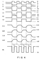
- Ink jet control pulse generator 3 specifically has a circuit construction as shown in Fig. 3.
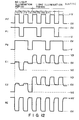
- a reference pulse signal labeled T in Fig. 4 is generated from pulse generator 31 and supplied to toggle terminal T of T-type flip-flop 32.
- T-type flip-flop 32 provides inverted output from its Q and Q terminals with the rising of reference pulse signal T.
- pulse signals having twice cycle period of reference pulse signal T and 180 degrees out of phase from one another as shown in Fig. 4 are provided from the Q and Q terminals of T-type flip-flop 32.
- the Q and Q outputs are amplified by respective operational amplifiers 33 and 34 before being supplied to the bases of power transistors 35 and 36, each of which has the emitter grounded and the collector connected through a resistor to a power supply of -V.
- Power transistors 35 and 36 are thus on-off operated according to the Q and Q outputs. Thus, they provided from their collectors first high voltage pulse signals Pi and P 2 which are 180 degrees out of phase with each other and are changed between 0 and -Vi volts.
- the Q and Q outputs are also supplied to the bases of power transistors 37 and 38, each of which has the emitter grounded and the collector connected through a resistor to a power supply of +V.
- Power transistors 37 and 38 are thus on-off operated according to the Q and Q outputs to provided, from their collectors, second high voltage pulse signals Pi' and P 2 ' which are 180 degrees out of phase with each other and are changed between 0 and Vi volts.
- Reference pulse signal T from pulse generator 31 is supplied through buffer 39 and photocoupler 40 to amplifier 41 for conversion into a high voltage pulse signal at double the frequency of high voltage pulse signals P 1 , P 1 ', P 2 and P 2 '.
- High voltage pulse signals Pi, P 1 ', P 2 , P2'and BE are applied respectively to first ink jet control electrode 18a, first auxiliary electrode 16a, second ink jet control electrode 18b, second auxiliary electrode 16b and back electrode 2.
- potentials E1d and E2d on first and second recording electrode groups 14a and 14b alternatively assume the maximum negative value as shown in Fig. 6A.
- potentials E2d and E1d on second and first recording electrode groups 14b and 14a alternatively assume the positive maximum value.
- the cycle period of application of high voltage pulse BE to back electrode 2 is one half that of high voltage pulses P 1 , P 2 , P 1 ' and R2', as shown in Fig. 4. Therefore, if photoconductive sections 15 are not illuminated by light, with the rising of pulse BE the potential difference between first recording electrode group 14a and back electrode 2 becomes maximum during periods TO and T2, while the potential different between second recording electrode group 14b and back electrode 2 is maximum during periods T1 and T3.
- oily ink 21 which is negatively charged is attracted to back electrode 2 by electrostatic forces alternately from first and second recording electrode groups 14a and 14b.
- the even and odd electrode groups in a plurality of recording electrodes arranged at a density of approximately 8 electrodes per mm in slit-like ink jet port 9 are driven alternatively to jet ink. It is thus possible to prevent ink from being jet from adjacent recording electrodes so as to disturb the direction of jetting of ink by electrostatic forces of repulsion acting on one another. In other words, ink will never be jet simultaneously from adjacent recording electrodes, so that there arises no problem of image deterioration due to repulsive forces of ink drops.
- in-phase high voltage pulse signals 180 degrees out of phase with respect to each other are applied respectively to first and second auxiliary electrodes 18a and 18b corresponding to control electrodesl8a and 18b. It is thus possible to increase the changes in the potentials on recording electrodes 16a and 16b without any breakdown caused in photoconductive sections 15, fixed resistors, etc.
- recording electrode potential V 1 d when high voltage V 1 is applied to auxiliary electrodes 16a and 16b is given as
- recording electrode potential V 2 d when high voltage -V i is applied to control electrodes 18a and 18b is given as In case of the presence of light illuminating photoconductive sections 15, with the resistance between each of auxiliary electrodes 16a and 16d and the corresponding one of recording electrodes 14a and 14b being reduced from Rd to Rp, recording electrode potential V i p when high voltage V i is applied to auxiliary electrodes 16a and 16b and recording electrode potential V 2 p when high voltage -V 1 is applied to control electrodes 18a and 18b are given respectively as
- recording electrode potential change AV can be made sufficiently large compared to the prior art case. It is thus possible to set the distance between the ink jet port and back electrode to be sufficiently large compared to the case of the prior art. This means that it is possible to form ink dots faith-fully on the recording sheet according to an optical signal for recording.
- auxiliary electrodes 16a and 16b, photoconductive sections 15, resistor films 19a and 19b and insulating film 17 were provided on substrate board 10 consisting of 2-mm thick glass plate processed to a predetermined shape, and then upper board 11 with ink jet control electrodes 18a and 18b and ink reservoir 20 provided in advance was overlapped via spacer 12 over and integrated with substrate board 10, thus obtaining ink recording head 1.
- Substrate board 10 consisted of a rectangular glass plate with a short side dimension of 50 mm and a long side dimension of 80 mm, with one long side having a wedge-like pointed sectional profile with an angle of approximately 15°, as shown in Fig. 7A, formed by polishing from one side.
- Upper board 11 like substrate board 10, consisted of a 2-mm thick rectangular glass plate with a short side dimension of 20 mm and a long side dimension of 100 mm and had a wedge-shaped long side obtained by polishing. It was also formed with a rectangular hole with a short side dimension of 2 mm and along side dimension of 50 mm, the hole serving as ink reservoir 20.
- each recording electrode 13 had its front and rear ends were respectively spaced apart by approximately 10 ⁇ m and 25 mm from the wedge-shaped edge of substrate board 10 and that also the distance from the rear end of first recording electrode group 14a to the front end of sections of comb-like auxiliary electrode 16a and the distance from the rear end of second recording electrode group 14b to the front end of sections of comb-like auxiliary electrode 16b were both 40 um.
- the width of recording electrodes 13 was set to 60 ⁇ m, and the pitch of arrangement of recording electrodes 13 was 125 ⁇ m.
- a nitrogen-containing amorphous silicon (a-Si:N) film was formed using glow discharge apparatus 100 as shown in Fig. 8, and then it was etched to form resistor films 19a and 19b and insulating film 17.
- the a-Si:N film was formed as follows. First, substrate board 10 was placed on sample support 103 also serving as glow discharge electrode provided in reaction vessel 101 of apparatus 100.
- silane gas (SiH 4 ) and nitrogen gas (N 2 ) were introduced in a volume ratio of approximately 1 : 6 from silane gas bomb 107 and nitrogen gas bomb 108, respectively, through gas mixer 109 into reaction vessel 101, and with the gas pressure in reaction vessel 101 held at approximately 1 Torr a glow discharge was induced by supplying high frequency power at a frequency of 13.56 MHz between planar electrode 104 and sample support 103 provided in reaction vessel 101.
- the a Si:N film was formed as a product of a plastic reaction between the silane gas and nitrogen gas on substrate board 10.
- the film thus formed had a thickness of approximately 4 ⁇ m.
- the unnecessary portion of the a-Si:N film formed on substrate board 10 was etched off as follows. A resist film was formed on the a-Si:N film, then substrate board 10 was placed again on sample support 103 of glow discharge apparatus as shown in Fig. 8, and a glow discharge was induced by introducing a mixture gas consisting of tetrafluoride methane gas (CF 4 ) and oxygen gas into reaction vessel 101.
- CF 4 tetrafluoride methane gas
- Auxiliary electrode 16b was formed by vacuum depositing, after the provision of resistor films 19a and 19b and insulating film 17 by the above process, a metallic chromium film on insulating film 17 and then etching the film.
- photoconductive films 15 were formed by depositing hydrated amorphous silicon (a-Si:H) using glow discharge apparatus 100 as in the case of the formation of the a-Si:N film. More specifically, the a-Si:H was formed to a thickness of 2 ⁇ m such that it bridges the end of each section of each of comb-like auxiliary electrodes 16a and 16b and the associated rear end of recording electrodes 13.
- the silane gas was introduced into reaction vessel 101 at a rate of 100 cc/min., the pressure in reaction vessel 101 was set to 1 Torr, high frequency power of 200 W was used, and substrate board 10 was heated for the deposition of a-Si:H to a temperature of 250°C using heater 105.
- first and second ink jet control electrodes 18a and 18b were provided such that they were parallel and spaced apart respectively by 2 and 8 mm from the wedge-shaped edge of upper board 11 (Fig. 7C).
- resistor films 19b provided to cover part of first recording electrode group 14a of substrate board 10 and second ink jet control electrode 18b face each other via oily ink 21 and that resistive films 19a provided to cover part of second recording electrode group 14b and first ink jet control eiectrode18a face each other via oily ink 21.
- First and second ink jet control electrodes 18a and 18b like the formation of recording electrodes 13 and auxiliary electrodes 16a and 16b, were formed by vacuum depositing a metallic chromium layer to a thickness of 1,500 angstrom on the surface of upper board 11 and etching this film.
- cylindrical back electrode 2 was disposed such that it was spaced apart via recording sheet 6 and extended parallel to slit-like ink jet port 9 of ink recording heat 1, and then ink reservoir 20 was filled with oily ink 21. Subsequently, the electric resistance between each of recording electrodes 13 and each of ink flying control electrodes 18a and 18b was measured using a needle-like probe in contact with recording electrode 13. Resistance Rc11 between first ink jet control electrode 18a and first recording electrode group 14a and 10 9 Q. Resistance Rc21 between first ink jet control electrode 18a and second recording electrode group 14b was 10 10 Q. Resistance Rc22 between second ink jet control electrode 18b and second recording electrode group 14b was 10 9 Q. Resistance Rc12 between second ink jet control electrode 18b and first recording electrode group 14a was 10 10 Q.
- a copying machine was constructed such that photoconductive sections 15 formed on substrate board 10 were illuminated by light reflected from original 4 through a self-focusing lens as optical means 5. Then, an original was illuminated by light from a light source (not shown), and in this state, 250-Hz high voltage pulse signals as shown at Pi and P 2 (with a peak of -200 V) and P 1 ' and P 2 ' (with a peak of +200 V) in Fig. 4 were applied respectively to ink flying control electrodes 18a and 18b and auxiliary electrodes 16a and 16b using electronic circuit shown in Fig. 3, while high voltage pulse signal BE with a peak value of +2,000 V, a frequency of 500 Hz and a pulse duration of 1 msec. was applied to back electrode 2. As a result, a clear copy image of original 4 consisting of oily ink 21 was formed on recording sheet 6.
- a coping machine was produced in the same manner as in Example 1 except for that 500 A thick a-Si:N protective film was deposition formed in the same manner as for resistor films 19a and 19b over the entire surface of auxiliary electrodes 16a and 16b except for power supply sections thereof after the provision of recording electrodes 13, auxiliary electrode 16a, resistor films 19a and 19b, insulating film 17 and auxiliary electrode 16b on substrate board 10 in the same manner as in Example 1.
- This copying machine was operated to produce satisfactory copy images under the same recording conditions as in Example 1 even in an atmosphere at a temperature of 30° C and with a relative humidity of 85 0 /o.
- the 500 A thick a-Si:N protective film formed on substrate board 10 was effective in preventing permeation of the a-Si:H film provided as photoconductive sections 15 with water and also preventing in the generation of electric field corrosion between first and second recording electrode groups 14a and 14b.
- a copying machine was produced in the same manner as in Example 1 using same ink recording heat 1 as in Example 1 except for that the a-Si:H film formed in the same manner as for the a-Si:H film as described before in conjunction with Example 1 was used as the material of resistor films 19a and 19b converting part of first and second recording electrode groups 14a and 14b on substrate board 10 and insulating film 17 covering auxiliary electrode 16a.
- this copying machine satisfactory copy images coupled be obtained by ink jet copying.
- the copying machine according to the invention it is possible to cause high voltage application to adjacent recording electrodes 13 at different timings to realize ink jet recording of satisfactory quality without need of complicated wiring of electrodes.
- the photoconductive sections may be made of a mateiral which mainly consists of Si atoms and contains Ge or halogen atoms. Further, photoconductive materials which mainly consist of Si atoms and contain slight quantities of borom (B) or phosphorus (P) atoms may be used suitably for the invention. Further, a-Si:H, GaAs and ZnSe containing fine silicon crystals, which are obtainable by causing the deposition of a plasmic reaction product on a substrate heated to approximately 400°C by inducing plasma discharge in a mixture gas consisting of silane gas (SiH 4 ) and hydrogen gas, are highly photoconductive and suited for the invention.
- the GaAs on substrate board 10, to be used for carrying out the invention can be obtained by causing a reaction of Gs(CH3)3 gas and AsH 3 gas by causing glow discharge in in the atmosphere of the mixture of these gases.
- the ZnSe film can be obtained by causing a reaction of the mixture of Zn(CH 3 ) 2 gas and SeH 2 gas in the manner as described above.
- the material for resistor films 19a and 19b and insulating film 17 may be used, in addition to nitrogen-containing amorphous silicon (a-Si:N) and oxygen-containing amorphous silicon, highly insulating materials such as carbon-containing amorphous silicon (a-Si:C) and amorphous silicon containing nitrogen and carbon (a-SiCN) with a metal cover film for forming auxiliary electrode 16b.
- a-Si:N nitrogen-containing amorphous silicon
- a-Si:C carbon-containing amorphous silicon
- a-SiCN amorphous silicon containing nitrogen and carbon
- the above materials may be produced by an ion plating process and a spattering process in addition to the ordinary plasmic reaction as shown above.
- auxiliary electrodes 16a and 16b were provided separately via insulating film 17, it is possible to use a single common auxiliary electrode by setting the cycle period of second high voltage pulse application to auxiliary electrode to be double the first high voltage pulse application cycle period.
- FIGs. 9 to 14A and 14B reference numerals like those in Figs. 1 to 8 designate like parts or portions, and detailed description thereof will be omitted.
- the system shown in Figs. 9 and 10 unlike the system shown in Figs.
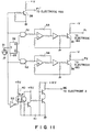
- High voltage pulse generator 3 in this embodiment has a circuit construction as shown in Fig. 11.
- Reference pulse signal T as shown in Fig. 12 is generated from pulse generator 31 and supplied to the base of power transistor 38, which has the emitter grounded and the collector connected through a resistor to power supply of V. Power transistor 38 thus is on-off operated according to reference pulse signal T and provides output P 1 ' as shown in Fig. 12 from the collector.
- Reference pulse signal T is also supplied to toggle terminal T of T-type flip-flop 32 and NANDs 51 and 52. With the rising of reference pulse T, T-type flip-flop 32 provides inversion outputs from its Q and Q terminals.
- pulse signals each of which has one half the pulse repetition frequency of reference pulse signal T and 180 degrees out of phase with each other, are pro vided from the Q and Q terminals of flip-flop 32 and supplied to NANDs 51 and 52, to which reference pulse signal T is also supplied.
- the outputs of NANDs 51 and 52 are amplified by operational amplifiers 33 and 34 before being applied to the bases of power transistors 35 and 36, which each have the emitter grounded and the collector connected through a resistor to power supply of -V. Power transistors 35 and 36 are thus on-offoperated according to the outputs of NANDs 51 and 52.
- Power transistors 35 and 36 thus provide from their collectors respective first high voltage pulse signals P 1 and P 2 , which have a reverse polarity of output P 1 ' are 180 degrees out of phase, i.e., shifted in a phase by an amount corresponding to the pulse width of reference pulse signal T and is changed from 0 to -Vi volts.
- Reference pulse signal T from pulse generator 53 is supplied through inverter 53 and photocoupler 40 to amplifier 41 for conversion into high voltage pulse signal BE, which has the same frequency as that of high voltage pulse signal P 1 ' but is 180 degrees out of phase with respect to high voltage pulse signal P 1 '.
- High voltage pulse signals P 1 , P 1 ', P 2 and BE are applied to first ink jet control electrode 18a, first auxiliary electrode 16a, second ink jet control electrode 18b and back electrode 2.
- auxiliary electrode 16a is held at a potential of +V volts, while first and second ink jet control electrodes 18a and 18b are held in the grounded state, i.e., at 0 V.
- first ink jet control electrode 18a is held at a potential of -V volts, and second ink jet control electrode 18b and auxiliary electrode 16a are held in the grounded state.
- first recording electrode group 14a is held at a potential, which is a division of the voltage of -V volts to the ratio between the resultant resistance of Rd and Rc12, i.e., Rd•Rc12/(Rd + Rc12), and Rc11.
- first and second ink jet control electrodes 18a and 18b are in the grounded state as in period T0, and also auxiliary electrode 16a is at a potential of +V volts.
- auxiliary electrode 16a is at a potential of +V volts.
- Second ink jet control electrode is held at a potential of -V volts, while first and second jet control electrodes 18a and auxiliary electrode 16a are held in the ground state.
- Second recording electrode group 14b thus is held at a potential, which is a division of the voltage of -V volts to the ratio of the resultant resistance of Rd and Rc21, i.e., Rd•Rc21/(Rd + Rc21) and Rc22.
- first and second recording electrode groups 14a and 14b during periods T4 to T7, during which photoconductive sections 15 are illuminated by any light, will be described.
- first and second recording electrode groups 14a and 14b and ink jet control electrode 16a Since photoconductive sections 15 are illuminated by light, the electric resistance between first and second recording electrode groups 14a and 14b and ink jet control electrode 16a is reduced to Rp, which is very low compared to the electric resistance Rd between first and second recording electrode groups 14a and 14b and auxiliary electrode 16a in the absence of light illuminating photoconductive sections 15. This is the sole difference, and equal voltages are applied to first and second ink jet control electrodes 18a and 18b and auxiliary electrode 16a during periods TO and T4, during periods T1 and T5, during periods T2 and T6 and during periods T3 and T7.
- first recording electrode group 14a is held at a potential, which is a division of the voltage of -V volts to the ratio of the resultant resistance of Rp and Rc12, i.e., Rp•Rc12/(Rp + Rc12), and Rc11.
- Second recording electrode group 14b is held at a potential, which is a division of the voltage of -V volts to the ratio of the resultant resistance of Rp and Rc22, i.e., Rp•Rc22/(Rp + Rc22).
- second link jet control electrode 18b is held at -V volts
- first ink jet control electrode 18a and auxiliary electrode 16a are both held in the grounded state.
- second recording electrode group 14b is at a potential, which is a division of the voltage of -V volts to the ratio of the resultant resistance of Rp and Rc21, i.e., Rp•Rc21/(Rp + Rc21) and Rc22
- first recording electrode group 14a is held at a potential, which is a division of the voltage of -V volts to the ratio of the resultant resistance of Rp and Rc11, i.e., Rp•Rc11/(Rp + Rc11) and Rc 12.
- first and second recording electrode groups 14a and 14b are both slightly negative.
- the potentials on first and second recording electrode groups 14a and 14b are thus varied as shown at E1 and E2 in Fig. 12, respectively.
- Fig. 13 shows an equivalent circuit concerning recording electrodes 13, auxiliary electrode 16 and ink jet control electrodes 18a and 18b.
- a high voltage of + HV as shown at BE in Fig. 12 is applied to back electrode 2.
- the electric field intensity between first recording electrode 14a and back electrode 2 assumes a maximum value, and ink 21 in the vicinity of the ends of first recording electrodes 14a is jet toward back electrode 2 to form ink dots on recording sheet 6.
- the electric field intensity between second recording electrode 14b and back electrode 2 assumes a maximum value, and ink 21 in the vicinity of the ends of second recording electrodes 14b is jet toward back electrode 2 form ink dots on recording sheet 6.
- Rc11 is the electric resistance between each of first recording electrodes 14a in slit-like jet port 9 and first ink jet control electrode 18a
- Rc12 is the electric resistance between each of second recording electrodes 14b and second ink jet control electrode 18b
- Rc21 is the electric resistance between each of second recording electrodes 14b and first ink jet control electrode 18a
- Rd is the electric resistance between each recording electrode 13 and auxiliary electrode 16a in the absence of light illuminating photoconductive sections 15
- Rp is the electric resistance between each recording electrode 13 and auxiliary electrode 16 in the presence of light illuminating photoconductive sections 15, it is possible to have the potentials on first and second recording electrodes 14a and 14b different form each other when a high voltage is applied to either one of first and second ink jet control electrodes 18a and 18b.
- the relation Rc11 ⁇ Rc12 can be met by making width W11 of the portions of recording electrode group 14a overlapping over first ink jet control electrode 18a to be greater than width W12 of the portions or recording electrode group 14a overlapping over second ink jet control electrode 18b such that S11 > S12.
- resistance Rc22 between second recording electrode group 14b and second ink jet control electrode 18b and resistance Rc21 between second recording electrode group 14b and first ink jet control electrode 18a can be met by making width W11 of the portions of recording electrode group 14a overlapping over first ink jet control electrode 18a to be greater than width W12 of the portions or recording electrode group 14a overlapping over second ink jet control electrode 18b such that S11 > S12.
- resistance Rc22 between second recording electrode group 14b and second ink jet control electrode 18b and resistance Rc21 between second recording electrode group 14b and first ink jet control electrode 18a can be met by making width W11 of the portions of recording electrode group 14a overlapping over first ink jet control electrode 18a to be greater than width W
- Rp and Rd can be given as
- Rd pped/t W ( ⁇ )
- pp ( ⁇ cm) and pd ( ⁇ cm) are respectively the volume resistivity of photoconductive sections 15 in the presence of light illuminating photoconductive sections 15 bridging recording electrodes 13 and auxiliary electrode 16 and that in the absence of any illuminating light
- t (cm) is the thickness of photoconductive sections
- d (cm) is the inter-electrode distance between the facing portions of recording electrodes 13 and auxiliary electrode 16
- W ( ⁇ ) is the width of electrodes.
- Rp and Rd thus can be set desirably by appropriately setting the values of d, t and W.
- the photoconductor to be used according to the invention is suitably one having a large difference between pp and ld.
- An example of such photoconductor is hydrated amorphous silicon.
- the high voltage pulse generator according to the invention is not limited to one as shown in Figs. 3 and 11, and the switching transistor may be obviously be replaced with a combination of an LC resonant circuit and a thyristor.
- Recording electrodes 13, auxiliary electrode 16 and photoconductive sections 15 were provided on slit-like ink jet port formation substrate board 10 obtained from a 2-mm thick glass plate, and slit-like ink jet port formation upper board 11, provided with first and second ink jet control electrodes 18a and 18b and ink reservoir 20, was overlapped via spacer 12 over and integrated with substrate board 10, whereby ink recording head 1 was obtained.
- Substrate board 10 consisted of a rectangular glass plate with a short side dimension of 50 mm and a long side dimension of 80 mm, with one long side having a wedge-like pointed sectional profile with an angle of approximately 15°, as shown in Fig. 7A, formed by polishing from one side.
- Upper board 11 like substrate board 10, consisted of a 2-mm thick rectangular glass plate with a short side dimension of 20 mm and a long side dimension of 100 mm and had a wedge-shaped long side obtained by polishing. It was also formed with a rectangular hole with a short side dimension of 2 mm and a long side dimension of 50 mm, the hole serving as ink reservoir 20.
- first and second ink jet control electrodes 18a and 18b having a width of 3 mm, were formed by etching a 1,500 A thick metallic chromium layer formed using a vacuum deposition apparatus on the surface of upper board 11 facing substrate board 10.
- Recording electrodes 13 and auxiliary electrode 16 were obtained by etching a 1,500 A thick metallic chromium layer formed using a vacuum deposition apparatus on the surface of substrate board 10. As shown schematically in Fig. 9, recording elec trodes 13 had partly varying widths.
- the etching was done such that the width of the portions of recording electrodes 14a where first recording electrodes 14a overlap over first ink jet control electrode 18a via the ink layer was 80 p.m, the width of the portions of recording electrodes 14a where first recording electrodes 14a overlap over second ink jet control electrode 18a via the ink layer was 4 ⁇ m, the width of the portions of recording electrodes 14b where second recording electrodes 14b overlap over second ink jet control electrode 18b via the ink layer was 80 ⁇ m, and the width of the portions of recording electrodes 14b where second recording electrodes 14b overlap over first ink jet control electrode 18a via the ink layer was 4 ⁇ m.
- each recording electrode 13 had its front and rear ends respectively spaced apart by approximately 10 ⁇ m and 25 mm from the wedge-shaped edge of substrate board 10 and that also the distance from the rear end of first recording electrode group 14a to the front end of sections of comb-like auxiliary electrode 16a and the distance from the rear end of second recording electrode group 14b to the front end of sections of comb-like auxiliary electrode 16a were both 40 um.
- a-Si:H hydrogen-containing amorphous silicon
- the a-Si:H film was formed as follows. First, substrate board 10 was placed on sample support 103 also serving as glow discharge electrode provided in reaction vessel 101 of apparatus 100. Then, after evacuating reaction vessel 101, silane gas (SiH 4 ) was introduced into reaction vessel 101, and with the gas pressure therein held at approximately 1 Torr a glow discharge was introduced by supplying high frequency power at a frequency of 13.56 MHz between planar electrode 104 and sample support 103 provided in reaction vessel 101. In this way, the a-Si:N film was formed as a product of a plasmic reaction between the silane gas and nitrogen gas on substrate board 10.
- silane gas SiH 4
- the silane gas was introduced into reaction vessel 101 at a rate of 100 cc/min., the pressure in reaction vessel 101 was set to 1 Torr, high frequency power of 200 W was used, and substrate board 10 was heated for the deposition of a-Si:H to a temperature of 250°C using heater 105.
- Ink jet control electrodes 18a and 18b were formed on slit-like ink jet port formation upper board 11 as follows. In order that ink jet control electrodes 18a and 18b respectively overlap increased width portions of recording electrodes 14a and 14b via oily ink 21 when overlapping upper board 11 over slit-like ink jet port formation substrate board 10 such that their wedge-shaped ends coincide, first and second ink jet control electrodes 18a and 18b were formed such that they were parallel, had a width of 3 mm and were spaced respectively by 2 and 8 mm from the wedge-shaped edge of upper board 11.
- First and second ink jet control electrodes 18a and 18b like recording electrodes 13 and auxiliary electrode 16, were formed by etching a 1,500 A metallic chromium layer vacuum deposited on upper board 11.
- Substrate board 10 and upper board 11 obtained in the above way were overlapped over each other via spacer 12 obtained from a 100- ⁇ m thick polyethylene telephthalate film and bonded together using an epoxy resin adhesive, thus obtaining ink recording head 1 having the shape as shown in Fig. 9.
- cylindrical back electrode 2 was disposed parallel to the slit-like ink jet port of ink recording head 1 via recording sheet 6, and ink reservoir 20 was filled with oily ink 21. Subsequently, the electric resistance between each recording electrode 13 and each of ink jet control electrodes 18a was measured with a needle-like probe in contact with recording electrode 13.
- Resistance Rc11 between first recording electrode 14a and first ink jet control electrode 18a was 10 9 Q
- resistance Rc12 between first recording electrode 14a and second ink jet control electrode 18b was 10 10 ⁇
- resistance Rc22 between second recording electrode 14b and second ink jet control electrode 18b was 10 9 ⁇
- resistance Rc21 between second recording electrode 14b and first ink jet control electrode 18a and 10 10 Q was 10 9 Q.
- a copying machine was constructed as shown in Fig. 10, such that light reflected from original 4 was projected through a self-focusing lens as optical means 5 onto photoconductive sections 15 provided on slit-like ink jet formation substrate board 10.
- a-Si:N nitrogen-containing amorphous silicon
- sample support 10 also serving as glow discharge electrode provided in reaction vessel 101 of apparatus 100 was placed slit-like ink jet port formation substrate board 10. Then, after evacuating reaction vessel 101, silane gas (SiH 4 ) and nitrogen gas (N 2 ) were introduced respectively from silane gas (SiH 4 ) bomb 107 and nitrogen gas bomb 108 in a volume ratio of 1 : 6 through gas mixer 109 into reaction vessel 101.
- silane gas (SiH 4 ) and nitrogen gas (N 2 ) were introduced respectively from silane gas (SiH 4 ) bomb 107 and nitrogen gas bomb 108 in a volume ratio of 1 : 6 through gas mixer 109 into reaction vessel 101.
- reaction vessel 101 held at approximately 1 Torr glow discharge was induced by supplying high frequency power at a frequency of 13.56 MHz between planar electrode 104 and sample support 10 provided in reaction vessel 101, thereby forming the nitrogen-containing amorphous silicon (a-Si:N) film as a plasmic reaction product of the silane gas and nitrogen gas on slit-like ink jet port formation substrate board 10.
- a-Si:N nitrogen-containing amorphous silicon
- the nitrogen-containing amorphous silicon (a-Si:N) was selectively etched off to leave portions over the portions of first and second recording electrodes 14a and 14b overlapping respective second and first ink jet control electrodes 18b and 18a via oily ink 21.
- the selective etching of the nitrogen-containing amorphous silicon (a-Si:N) was done as follows. A resist film was formed on the nitrogen-containing amorphous silicon (a-Si:N) film, then slit-like ink jet port formation substrate board 10 was placed again on sample support 103 of glow discharge apparatus shown in Fig. 8, and then glow discharge was induced by introducing a mixture gas consisting of tetrafluoride methane gas (CF 4 ) and oxygen gas into reaction vessel 101.
- CF 4 tetrafluoride methane gas
- the distance from the rear end of recording electrodes 13 to the front end of the sections of comb-like auxiliary electrode 16 in this example was set to be 40 ⁇ m as in previous Example 1. Then, like Example 1 a hydrogen-containing amorphous silicon (a-Si:H) was formed to bridge recording electrodes 13 and auxiliary electrode 16, thus obtaining ink recording head 1.
- a-Si:H hydrogen-containing amorphous silicon
- resistance Rc11 between each first recording electrode 14a and ink jet control electrode 18a was 10 9 Q
- resistance Rc12 between each first recording electrode 14a and second ink jet control electrode 18b was 5 x 10 10 ⁇
- resistance Rc22 between each second recording electrode 14b and second ink jet control electrode was 10 9 Q
- resistance Rc21 between each second recording electrode 14b and ink jet control electrode 18a was 5 x 10 10 Q.
- This copying machine was operated to obtain satisfactory copy images under the same conditions as Example 1 even in an atmosphere at a temperature of 30° C and with a relative humidity of 85% and subject to ready changes in the resistivity of the oily ink.
- An ink recording head was fabricated in the same manner as in Example 5 except for those portions of recording electrodes 13 in contact with oily ink 21 were covered by a 500 A thick nitrogen-containing amorphous silicon, and the same copying machine as shown in Examples 4 and 5 was produced. Then, in the absence of light illuminating photoconductive sections 15 of the copying machine, the same voltage pulse signals as in Example 4 were applied to ink jet control electrodes 18a and 18b, auxiliary electrode 16 and back . electrode 2. In consequence, ink was caused to fly alternatively from the ends of recording electrodes 14a and 14b toward recording sheet 6. After performing recording operation for a total of 100 hours, the ends of the recording electrodes were observed using a microscope to recognize no trace of electrolytic corrosion at the ends of the recording electrodes.
- the 500 A thick nitrogen-containing amorphous silicon (a-Si:N) film provided on slit-like ink jet port formation substrate board 10 in the embodiment has an effect of preventing the migration of water into the hydrate amorphous silicon (a-Si:H) provided on photoconductive sections 15 and generation of electrolytic corrosion occurring between recording electrodes 14a and 14b.
- Recording electrodes 13 and auxiliary electrodes 16 having the same shape as Example 4 were provided on slit-like ink jet port formation substrate board 10, and then portions of first and second recording electrodes 14a and 14b overlapping over second and first ink jet control electrodes 18b and 18a via oily ink 21, i.e., 4- ⁇ m wide portions of recording electrodes 14a and 14b, were covered by a 4- ⁇ m thick nitrogen-containing amorphous silicon (a-Si:N) film.
- the nitrogen-containing amorphous silicon (a-Si:N) film was deposited like the hydrogen-containing amorphous silicon (a-Si:H) film using glow discharge apparatus 100 shown in Fig. 8.
- slit-like ink jet port of motion substrate board 10 was placed on sample support 103 also serving glow discharge electrode provided reaction vessel 101 of apparatus 100, then after evacuating reaction vessel 101 silane gas (SiH 4 ) and nitrogen gas (N 2 ) were introduced respectively from silane gas bomb 107 and nitrogen gas bomb 108 in a volume ratio of 1 : 6 through a gas mixer 109 into reaction vessel 101, and then with the gas pressure in reaction vessel 101 held at approximately 1 Torr glow discharge was induced by supplying high frequency power of 13.56 MHz between planar electrode 104 and sample support 103 also serving as glow discharge electrode in reaction vessel 101.
- the nitrogen-containing amorphous silicon (a-Si:N) film was formed as a product of plasmic reaction product between silane gas (SiH 4 ) and nitrogen gas (N 2 ).
- the nitrogen-containing amorphous silicon (a-Si:N) film was selectively etched off to leave portions other than the portions through which first and second recording electrodes 14a and 14b are faced to respective first and second ink jet control electrodes 18a and 18b.
- the selective etching of the nitrogen-containing amorphous silicon (a-Si:N) was done as follows. A resist film was formed on the nitrogen-containing amorphous silicon (a-Si:N), then slit-like ink jet port formation substrate board 10 was placed on sample support 103 of glow discharge apparatus 100 as shown in Fig. 8, and glow discharge was induced by introducing a mixture gas consisting of tetrafluoride methane gas (CF 4 ) and oxygen gas (0 2 ) into reaction vessel 101.
- CF 4 tetrafluoride methane gas
- an ink jet copying machine which was entirely the same as in Example 4 except for a nitrogen-containing amorphous silicon (a-Si:N) was formed on predetermined portions of recording electrodes 14a and 14b.
- a-Si:N nitrogen-containing amorphous silicon
- resistance Rc11 between first recording electrode 14a and first ink jet control electrode 18a was 10 9 ⁇
- resistance Rc12 between first recording electrode 14a and second ink jet control electrode 18b was 10 10 ⁇
- resistance Rc22 between second recording electrode 14b and second ink jet control electrode 18b was 10 9 ⁇
- resistance Rc21 between second recording electrode 14b and first ink jet control electrode 18a was 10 10 Q.
- This copying machine was operated to obtain satisfactory copy images under the same conditions as in Example 4 even in an atmosphere at a temperature of 30° C, with a relative humidity of 85% and readily subject to changes in the resistivity of oily ink 21.
- the ink jet copying machine of electrostatic acceleration type makes use of a change in the conductivity of the photoconductive sections connected to recording electrodes induced by illumination of the photoconductors by light for changing the recording electrode potential in the form of pulses.
- the photoconductive section may be made of material consisting of Si atoms as base material and containing Ge atoms of halogen atoms as well as hydrate amorphous silicon (a-Si:H), and materials consisting of Si atoms as base material and slightly containing B atoms and P atoms may be also used for photoconductive section suited for the invention.
- hydrate amorphous silicon (a-Si:H) containing fine crystals of silicon obtained by inducing plasma discharge in a mixture gas consisting of silane gas (SiH 4 ) and hydrogen gas (H 2 ) and causing deposition of a resultant plasmic reaction product on a substrate heated to approximately 400° C as well as GaAs and ZnSe is highly photoconductive and can be used for the invention.
- the deposition of the GaAs film on the slit-like ink jet port formation substrate board 10 used for the invention was obtained by causing reaction of Ga(CH 3 ) 3 gas and AsH 3 gas through glow discharge caused in the atmosphere of the mixture gas of these two gases.
- the ZnSe film was obtained by causing reaction of Zn(CH 3 ) 3 gas and SeH 2 gas in the same manner as above.
- the material of insulating films 19a and 19b may be highly electrically insulating films of carbon-containing amorphous silicon (a-Si:C) and amorphous silicon containing nitrogen and carbon (a-SiCN) as well as nitrogen-containing amorphous silicon (a-Si:N) and carbon-containing amorphous silicon (a-Si:C) as shown in the examples of the invention. These materials may be obtained by the ion plating process and spattering process in addition to the ordinary plasmic reaction used in the above embodiment.
- the light reflected form the original is directed to the photoconductive sections through the self-focusing lens, but it is also possible to use an optical system using a mirror or a lens for projecting the light reflected from the original.
- an ink jet copying machine capable of enlargement and contraction.
- ink jet printers wherein LED elements arranged at a high density above photoconductive sections are on-off operated according to recording data, or shutters consisting of a liquid crystal or the like and provided between a light source and photoconductive sections are on-off operated according to recording data.
- recording electrodes 14a and 14b on the end of substrate board 10 are covered by insulating film 55. Since recording electrodes are covered by insulating layer 55, even if a wave is generated on the surface of ink at the ink jet port when a high pulse voltage is applied between recording electrodes 14a and 14b and back electrode 2 to expose the substrate board surface, recording electrodes 14a and 14b are not directly exposed to air, and it is possible to produce a spark discharge with respect to back electrode 2.
- Recording electrodes 13 having a width of 60 ⁇ m and arranged at a pitch of 125 ⁇ m were formed on substrate board 10 made of glass by forming and selectively etching a 1,500 A metallic chromium layer. Recording electrodes 13, as shown in Fig. 15, were formed such that they are spaced apart by approximately 30 ⁇ .tm from polished wedge-shaped end 18 of substrate board 10. The surface of recording electrodes 13 was covered by 1,000 A thick insulating film 55 of SisN 4 formed by the plasmic polymerization reaction. Upper board 11 was placed over substrate board 10 having the above structure via spacer 12, and these components were integrated using an epoxy resin adhesive, thus obtaining ink recording head 1.
- Back electrode 2 of stainless steel and having a diameter of 20 mm was disposed such that it is disposed by a distance of 0.4 mm from slit-like ink jet port 9 of ink recording head 1, and ink reservoir 20 was filled with oily ink 21 with an electric conductivity of 10- 9 ⁇ -1 /cm -1 .
- a high voltage pulse signal having a pulse width of 0.5 msec., a peak value of +2,000 V and a repetition frequency of 1 kpps was applied to back electrode 2. No spark discharge occurred between recording electrode 13 and back electrode 2 until +2,600 V was reached by the peak value of the high voltage pulse signal applied to back electrode 2.
- Ink recording head 1 was fabricated in the same manner as in Example 4 except for that recording electrodes 13 were spaced apart by 5 ⁇ .tm from end face 20 and that a-Si:C insulating film 55 with a thickness of 2 ⁇ m was formed by plasmic polymerization reaction on the surface of recording electrodes 13. With a copying machine using this ink recording head, no spark discharge occurred even by increasing the potential difference between recording electrodes 13 and back electrode 2 to 2,900 V.
- Ink recording head 1 was fabricated in the same manner as in Example 2 except for that 500 A SiN insulating film 14 was formed by plasmic polymerization rection on the surface of recording electrodes 13. With a copying machine using this ink recording head, no spark discharge occurred by increasing the potential difference between recording electrodes 13 and back electrode 2 to 2,350 V.
- recording electrodes 13 are provided such that their ends are on the inner side of end face 13 of substrate board 13.
- the end portions of recording electrodes 10 were covered not only by insulating film 55 but also by oily ink 20, whereby it is possible to obtain the effect of spark discharge prevention.
- the end of recording electrodes 13 is suitable spaced apart by 5 to 300 um form the end of the substrate board.
- the recording electrodes 13 may be made of other insulating materials as Si0 2 , Ti0 2 , A2 2 0a, BN and AeN instead of SiC and SiN to obtain the same effects.
Landscapes
- Particle Formation And Scattering Control In Inkjet Printers (AREA)
Applications Claiming Priority (6)
| Application Number | Priority Date | Filing Date | Title |
|---|---|---|---|
| JP61265455A JP2602817B2 (ja) | 1986-11-10 | 1986-11-10 | インク記録方法 |
| JP265455/86 | 1986-11-10 | ||
| JP16307987 | 1987-06-30 | ||
| JP163078/87 | 1987-06-30 | ||
| JP16307887A JPS648050A (en) | 1987-06-30 | 1987-06-30 | Electrostatic acceleration type ink jet recorder |
| JP163079/87 | 1987-06-30 |
Publications (2)
| Publication Number | Publication Date |
|---|---|
| EP0267782A2 true EP0267782A2 (fr) | 1988-05-18 |
| EP0267782A3 EP0267782A3 (fr) | 1989-09-27 |
Family
ID=27322104
Family Applications (1)
| Application Number | Title | Priority Date | Filing Date |
|---|---|---|---|
| EP87309942A Withdrawn EP0267782A3 (fr) | 1986-11-10 | 1987-11-10 | Système à jet d'encre |
Country Status (2)
| Country | Link |
|---|---|
| US (1) | US4794463A (fr) |
| EP (1) | EP0267782A3 (fr) |
Cited By (2)
| Publication number | Priority date | Publication date | Assignee | Title |
|---|---|---|---|---|
| EP0750989A3 (fr) * | 1995-06-29 | 1997-02-26 | Nec Corp | Tête d'impression électrostatique à jet d'encre avec structure d'électrode empilée |
| EP0771654A1 (fr) * | 1995-10-30 | 1997-05-07 | Nec Corporation | Tête d'impression à jet d'encre électrostatique |
Families Citing this family (20)
| Publication number | Priority date | Publication date | Assignee | Title |
|---|---|---|---|---|
| US5070410A (en) * | 1989-03-21 | 1991-12-03 | Hewlett-Packard Company | Apparatus and method using a combined read/write head for processing and storing read signals and for providing firing signals to thermally actuated ink ejection elements |
| US5162916A (en) * | 1990-07-02 | 1992-11-10 | Xerox Corporation | Compact read/write scanner |
| US5619234A (en) * | 1993-03-15 | 1997-04-08 | Kabushiki Kaisha Toshiba | Ink-jet recording apparatus which allows shifting or changing of ink position or direction |
| JP2783208B2 (ja) * | 1995-08-28 | 1998-08-06 | 日本電気株式会社 | 静電式インクジェット記録装置 |
| EP0786344B1 (fr) * | 1996-01-29 | 2000-05-24 | Nec Corporation | Tête d'impression électrostatique simple et économique |
| JPH106506A (ja) * | 1996-04-23 | 1998-01-13 | Seiko Instr Inc | 記録装置並びに該装置に用いる記録ユニット及び記録ヘッド |
| US6123416A (en) * | 1996-07-31 | 2000-09-26 | Nec Corporation | Inkjet apparatus and method for ejecting particulate matter from an ejection electrode using an electric field |
| JPH1086382A (ja) * | 1996-09-13 | 1998-04-07 | Seiko Instr Inc | 記録装置並びに該装置に用いる記録ユニット |
| GB9706069D0 (en) | 1997-03-24 | 1997-05-14 | Tonejet Corp Pty Ltd | Application of differential voltage to a printhead |
| EP0869003B1 (fr) * | 1997-04-03 | 2002-02-27 | Nec Corporation | Dispositif électrostatique d'enregistrement à jet d'encre |
| US6402299B1 (en) | 1999-10-22 | 2002-06-11 | Lexmark International, Inc. | Tape automated bonding circuit for use with an ink jet cartridge assembly in an ink jet printer |
| GB2357464A (en) * | 1999-12-21 | 2001-06-27 | Fuji Photo Film Co Ltd | Ink jet printing method and apparatus |
| US6747684B2 (en) | 2002-04-10 | 2004-06-08 | Hewlett-Packard Development Company, L.P. | Laser triggered inkjet firing |
| US7083250B2 (en) * | 2002-06-07 | 2006-08-01 | Hewlett-Packard Development Company, L.P. | Fluid ejection and scanning assembly with photosensor activation of ejection elements |
| US6799819B2 (en) | 2002-06-07 | 2004-10-05 | Hewlett-Packard Development Company, L.P. | Photosensor activation of an ejection element of a fluid ejection device |
| US7104623B2 (en) * | 2002-06-07 | 2006-09-12 | Hewlett-Packard Development Company, L.P. | Fluid ejection system with photosensor activation of ejection element |
| US6705701B2 (en) * | 2002-06-07 | 2004-03-16 | Hewlett-Packard Development Company, L.P. | Fluid ejection and scanning system with photosensor activation of ejection elements |
| US6981758B2 (en) | 2003-07-30 | 2006-01-03 | Hewlett-Packard Development Company, L.P. | Photonically activated fluid dispensing system and methods |
| JP4773360B2 (ja) * | 2003-11-17 | 2011-09-14 | コーニンクレッカ フィリップス エレクトロニクス エヌ ヴィ | 流体を操作するためのシステム |
| JP2006175743A (ja) * | 2004-12-22 | 2006-07-06 | Canon Inc | 記録装置、インクミスト回収方法、及び記録方法 |
Family Cites Families (6)
| Publication number | Priority date | Publication date | Assignee | Title |
|---|---|---|---|---|
| US3553719A (en) * | 1967-12-18 | 1971-01-05 | Matsushita Electric Industrial Co Ltd | Printing device of modulation on faceplate of cathode-ray tube |
| JPS6059869B2 (ja) * | 1979-06-22 | 1985-12-27 | 日本電信電話株式会社 | インク記録用ヘツド |
| US4271416A (en) * | 1978-10-18 | 1981-06-02 | Nippon Telegraph And Telephone Public Corporation | Slit type ink recording apparatus |
| JPS56170A (en) * | 1979-06-15 | 1981-01-06 | Nippon Telegr & Teleph Corp <Ntt> | Ink recording system |
| JPS56167476A (en) * | 1980-05-30 | 1981-12-23 | Nippon Telegr & Teleph Corp <Ntt> | Application of recording voltage |
| JPS60250962A (ja) * | 1984-05-29 | 1985-12-11 | Toshiba Corp | 静電加速型インクジエツト記録装置 |
-
1987
- 1987-11-10 EP EP87309942A patent/EP0267782A3/fr not_active Withdrawn
- 1987-11-10 US US07/118,883 patent/US4794463A/en not_active Expired - Fee Related
Cited By (4)
| Publication number | Priority date | Publication date | Assignee | Title |
|---|---|---|---|---|
| EP0750989A3 (fr) * | 1995-06-29 | 1997-02-26 | Nec Corp | Tête d'impression électrostatique à jet d'encre avec structure d'électrode empilée |
| US5969732A (en) * | 1995-06-29 | 1999-10-19 | Nec Corporation | Electrostatic ink-jet recording device with control electrodes for selectively preventing ejection of toner |
| EP0771654A1 (fr) * | 1995-10-30 | 1997-05-07 | Nec Corporation | Tête d'impression à jet d'encre électrostatique |
| US5975684A (en) * | 1995-10-30 | 1999-11-02 | Nec Corporation | Ink jet recording head having an ink stream path |
Also Published As
| Publication number | Publication date |
|---|---|
| EP0267782A3 (fr) | 1989-09-27 |
| US4794463A (en) | 1988-12-27 |
Similar Documents
| Publication | Publication Date | Title |
|---|---|---|
| EP0267782A2 (fr) | Système à jet d'encre | |
| US4155093A (en) | Method and apparatus for generating charged particles | |
| US5404157A (en) | Apparatus for generating ions in solid ion recording head with improved stability | |
| JPH0656512B2 (ja) | イオン投射複写機 | |
| US4137537A (en) | Electrostatic transfer process and apparatus for carrying out the same | |
| GB2038719A (en) | Image recording apparatus | |
| US5717449A (en) | Toner projection printer with improved address electrode structure | |
| US5296878A (en) | Apparatus for generating ions in solid ion recording head with improved stability | |
| EP0963852B1 (fr) | Méthode d'impression et contrôle pour une tête d'impression avec électrodes de déviation pour l'impression électrostatique directe | |
| JPS6213379A (ja) | インクジエツト記録方法 | |
| JP3176943B2 (ja) | 固体イオン発生器 | |
| JP3093320B2 (ja) | イオン発生器 | |
| JPS62127249A (ja) | 静電加速型インクジエツト記録装置 | |
| JPH04164661A (ja) | 静電記録装置 | |
| EP0983858B1 (fr) | Méthode d'impression et contrôle pour une tête d'impression avec système d'électrodes de déviation pour l'impression électrostatique directe | |
| JPS6280048A (ja) | 記録装置 | |
| JP2602817B2 (ja) | インク記録方法 | |
| EP0963853B1 (fr) | Méthode d'impression dans un appareil d'impression électrostatique directe ayant une structure de tête d'impression avec électrodes de déflexion et moyens de contrôle électrique pour cettes électrodes de déflexion | |
| JPS62148270A (ja) | 記録装置 | |
| JPS623963A (ja) | 静電加速型インクジエツト記録装置 | |
| JPH05278258A (ja) | イオン発生器 | |
| Tuan | Printing applications of a-Si thin film transistors | |
| JPS62227754A (ja) | 静電加速型インクジエツト記録装置 | |
| JPS61286150A (ja) | インジエツト記録装置 | |
| JP2831669B2 (ja) | コロナイオン記録装置 |
Legal Events
| Date | Code | Title | Description |
|---|---|---|---|
| PUAI | Public reference made under article 153(3) epc to a published international application that has entered the european phase |
Free format text: ORIGINAL CODE: 0009012 |
|
| 17P | Request for examination filed |
Effective date: 19880211 |
|
| AK | Designated contracting states |
Kind code of ref document: A2 Designated state(s): DE FR GB |
|
| PUAL | Search report despatched |
Free format text: ORIGINAL CODE: 0009013 |
|
| AK | Designated contracting states |
Kind code of ref document: A3 Designated state(s): DE FR GB |
|
| 17Q | First examination report despatched |
Effective date: 19910801 |
|
| STAA | Information on the status of an ep patent application or granted ep patent |
Free format text: STATUS: THE APPLICATION IS DEEMED TO BE WITHDRAWN |
|
| 18D | Application deemed to be withdrawn |
Effective date: 19920811 |
|
| RIN1 | Information on inventor provided before grant (corrected) |
Inventor name: YAMAZAKI, MUTSUKI Inventor name: TAMURA, SAKAE Inventor name: OKUYAMA, TETSUO Inventor name: UEHARA, TSUTOMU |