EP0268181A1 - Boîtier moulé en matière plastique avec grille de fiches pour dispositif à circuits intégrés - Google Patents
Boîtier moulé en matière plastique avec grille de fiches pour dispositif à circuits intégrés Download PDFInfo
- Publication number
- EP0268181A1 EP0268181A1 EP87116524A EP87116524A EP0268181A1 EP 0268181 A1 EP0268181 A1 EP 0268181A1 EP 87116524 A EP87116524 A EP 87116524A EP 87116524 A EP87116524 A EP 87116524A EP 0268181 A1 EP0268181 A1 EP 0268181A1
- Authority
- EP
- European Patent Office
- Prior art keywords
- pins
- chip
- carrier member
- plastic molded
- plastic
- Prior art date
- Legal status (The legal status is an assumption and is not a legal conclusion. Google has not performed a legal analysis and makes no representation as to the accuracy of the status listed.)
- Granted
Links
Images



Classifications
-
- H—ELECTRICITY
- H10—SEMICONDUCTOR DEVICES; ELECTRIC SOLID-STATE DEVICES NOT OTHERWISE PROVIDED FOR
- H10W—GENERIC PACKAGES, INTERCONNECTIONS, CONNECTORS OR OTHER CONSTRUCTIONAL DETAILS OF DEVICES COVERED BY CLASS H10
- H10W76/00—Containers; Fillings or auxiliary members therefor; Seals
- H10W76/10—Containers or parts thereof
- H10W76/12—Containers or parts thereof characterised by their shape
- H10W76/15—Containers comprising an insulating or insulated base
- H10W76/153—Containers comprising an insulating or insulated base having interconnections in passages through the insulating or insulated base
-
- H—ELECTRICITY
- H10—SEMICONDUCTOR DEVICES; ELECTRIC SOLID-STATE DEVICES NOT OTHERWISE PROVIDED FOR
- H10W—GENERIC PACKAGES, INTERCONNECTIONS, CONNECTORS OR OTHER CONSTRUCTIONAL DETAILS OF DEVICES COVERED BY CLASS H10
- H10W70/00—Package substrates; Interposers; Redistribution layers [RDL]
- H10W70/60—Insulating or insulated package substrates; Interposers; Redistribution layers
- H10W70/62—Insulating or insulated package substrates; Interposers; Redistribution layers characterised by their interconnections
- H10W70/63—Vias, e.g. via plugs
- H10W70/635—Through-vias
-
- H—ELECTRICITY
- H10—SEMICONDUCTOR DEVICES; ELECTRIC SOLID-STATE DEVICES NOT OTHERWISE PROVIDED FOR
- H10W—GENERIC PACKAGES, INTERCONNECTIONS, CONNECTORS OR OTHER CONSTRUCTIONAL DETAILS OF DEVICES COVERED BY CLASS H10
- H10W76/00—Containers; Fillings or auxiliary members therefor; Seals
- H10W76/40—Fillings or auxiliary members in containers, e.g. centering rings
- H10W76/42—Fillings
- H10W76/47—Solid or gel fillings
-
- H—ELECTRICITY
- H10—SEMICONDUCTOR DEVICES; ELECTRIC SOLID-STATE DEVICES NOT OTHERWISE PROVIDED FOR
- H10W—GENERIC PACKAGES, INTERCONNECTIONS, CONNECTORS OR OTHER CONSTRUCTIONAL DETAILS OF DEVICES COVERED BY CLASS H10
- H10W70/00—Package substrates; Interposers; Redistribution layers [RDL]
- H10W70/60—Insulating or insulated package substrates; Interposers; Redistribution layers
- H10W70/67—Insulating or insulated package substrates; Interposers; Redistribution layers characterised by their insulating layers or insulating parts
- H10W70/68—Shapes or dispositions thereof
- H10W70/682—Shapes or dispositions thereof comprising holes having chips therein
-
- H—ELECTRICITY
- H10—SEMICONDUCTOR DEVICES; ELECTRIC SOLID-STATE DEVICES NOT OTHERWISE PROVIDED FOR
- H10W—GENERIC PACKAGES, INTERCONNECTIONS, CONNECTORS OR OTHER CONSTRUCTIONAL DETAILS OF DEVICES COVERED BY CLASS H10
- H10W74/00—Encapsulations, e.g. protective coatings
-
- H—ELECTRICITY
- H10—SEMICONDUCTOR DEVICES; ELECTRIC SOLID-STATE DEVICES NOT OTHERWISE PROVIDED FOR
- H10W—GENERIC PACKAGES, INTERCONNECTIONS, CONNECTORS OR OTHER CONSTRUCTIONAL DETAILS OF DEVICES COVERED BY CLASS H10
- H10W90/00—Package configurations
- H10W90/701—Package configurations characterised by the relative positions of pads or connectors relative to package parts
- H10W90/731—Package configurations characterised by the relative positions of pads or connectors relative to package parts of die-attach connectors
- H10W90/737—Package configurations characterised by the relative positions of pads or connectors relative to package parts of die-attach connectors between a chip and a laterally-adjacent lead frame, conducting package substrate or heat sink
-
- H—ELECTRICITY
- H10—SEMICONDUCTOR DEVICES; ELECTRIC SOLID-STATE DEVICES NOT OTHERWISE PROVIDED FOR
- H10W—GENERIC PACKAGES, INTERCONNECTIONS, CONNECTORS OR OTHER CONSTRUCTIONAL DETAILS OF DEVICES COVERED BY CLASS H10
- H10W90/00—Package configurations
- H10W90/701—Package configurations characterised by the relative positions of pads or connectors relative to package parts
- H10W90/751—Package configurations characterised by the relative positions of pads or connectors relative to package parts of bond wires
- H10W90/753—Package configurations characterised by the relative positions of pads or connectors relative to package parts of bond wires between laterally-adjacent chips
-
- H—ELECTRICITY
- H10—SEMICONDUCTOR DEVICES; ELECTRIC SOLID-STATE DEVICES NOT OTHERWISE PROVIDED FOR
- H10W—GENERIC PACKAGES, INTERCONNECTIONS, CONNECTORS OR OTHER CONSTRUCTIONAL DETAILS OF DEVICES COVERED BY CLASS H10
- H10W90/00—Package configurations
- H10W90/701—Package configurations characterised by the relative positions of pads or connectors relative to package parts
- H10W90/751—Package configurations characterised by the relative positions of pads or connectors relative to package parts of bond wires
- H10W90/754—Package configurations characterised by the relative positions of pads or connectors relative to package parts of bond wires between a chip and a stacked insulating package substrate, interposer or RDL
Definitions
- the present invention is directed to a plastic molded pin grid chip carrier package, and more particularly to a plastic molded chip carrier package having an increased number of I/O pins arranged in a pin grid array.
- Pin grid array packages for semiconductor chips have been widely accepted in the art to replace ceramic packages for their feasibility of incorporating a plurality of I/O pins at the time of molding the package and for thermal compatibility with a conventional printed-circuit boards on which the packages are frequently required to be directly mounted.
- Such pin grid array plastic packages have been proposed, for example, in U.S. Pat. No. 4,618,739 in which a chip carrier is molded from a suitable plastic material to integrally include a plurality of I/O pins.
- the conventional pin grid array configuration as in the above patent will encounter with a critical problem when adding or increasing the number of I/O pins while retaining the pin density as high as possible for avoiding the package from becoming too large.
- the problem is that, as the number of rows on the pin grid is increased to give a more number of I/O pins in compliance with the increased I/O ports on the chip but without substantially increasing the pin pitch in each row, the electrical interconnection between the I/O ports on the chip and the individual I/O pins requires an elaborate wiring or connection technique, which is rather difficult to be realized on the pin grid array even with a standard pin pitch of 100 mil.
- the prior pin grid array package has a certain limitation on increasing the number of rows on the pin grid array, making the package unsatisfactory when it is required to further increase the number of I/O pin without substantially increasing the pin pitch.
- the present invention which includes a carrier member made of a plastic material with a rectangular chip recess for mounting an integrated circuit chip and a plurality of I/O pins having its top end portions integrally embedded into the carrier member outwardly of the chip recess and protruding downwardly from the carrier member.
- the characterizing feature of the present invention resides in that the I/O pins are arranged in plural rows in such a manner that the I/O pins in each of the rows are uniformly spaced apart along the sides of said chip recess and are uniformly staggered with respect to the I/O pins in the adjacent row.
- two versions of the packages are disclosed, one utilizing wire elements and the other a plastic substrate with a trace pattern of conductor lines for electrical interconnection between the I/O pins and the corresponding I/O ports on the chip.
- the former version therefore, the above staggered arrangement of the I/O pins allows the interconnection to be easily made by usual wire bonding technique.
- the latter version it is allowed to design a rather simple pattern of the conductor lines on the plastic substrate by the use of the staggered arrangement.
- each of the I/O pins is mounted in the carrier member with its top recessed from the top surface of the carrier member so as to form thereat a solder pit for receiving a solder by which the I/O pin is electrically connected to the corresponding conductor line on the plastic substrate.
- solder is retained in the individual pits and is prevented from accidentally flowing to the non-target lines or I/O pins, improving the reliability in the electrical connection therebetween.
- the conductor lines of the plastic substrate are each formed with a solder bump which fits in the solder pit of the carrier member prior to the reflow soldering thereof to the corresponding I/O pins.
- the solder pits therefore, serve to properly register the solder bump with the corresponding I/O pins, in addition to retaining the solder therein for preventing it from reaching the non-target lines.
- the plastic substrate is preferably formed from a thermosetting plastic material of inherently high thermal resistance so that it can be kept unaffected at the time of soldering the conductor lines to the I/O pins and also at the time of soldering the I/O pins to the circuit on a circuit board on which the package is mounted.
- a transparent material is used to seal the chip and its electrical connection to the I/O pins. This is most advantageous when it is required to expose the chip to light or ultraviolet light after encapsulating the chip as in the case where a semiconductor chip such as CCD or EPROM is utilized as the chip.
- a plastic molded plastic chip carrier package in accordance with a first preferred embodiment of the present invention.
- the package comprises a flat shaped carrier member 10 having a center recess 11 for mounting therein a semiconductor chip 1 , a plurality of I/O pins 20 arranged on a pin grid to extrude from the bottom surface of the carrier member 10 .
- the carrier member 10 is molded from a suitable heat resistive thermoplastic or thermosetting plastic material into a flat rectangular configuration by a conventional injection or transfer molding technique.
- Suitable heat-resistive thermoplastic material includes polyphenylene sulphide, polysulphone, polyethersulphone, and polyarylsulphone.
- Suitable thermosetting plastic material includes phenol, polyimide, and epoxy resins.
- the I/O pins 20 are molded in the carrier member 10 with their top ends projected slightly above the top surface thereof and present a pin grid array arranged in the peripheral portion of the carrier member 10 outwardly of the rectangularly shaped center recess 11 .
- Each of the I/O pins 20 has a pair of spaced shoulders 21 and 22 on its top portion both of which are anchored in the molded carrier member 10 for enhanced mechanical bonding strength thereto.
- the pin grid array comprises two rows of the I/O pins 20 arranged on each of the four sides of the carrier member 10.
- the I/O pins 20 in each row are spaced on 100-mil centers and staggered with respect to those in the adjacent row so that only one of the I/O pins 20 in one row is located along the spacing between the two adjacent I/O pins 20 in the other row.
- Each of the I/O pins 20 are electrically interconnected to the individual pads or I/O ports 2 on the chip 1 by a wire element 3 utilizing a known wire bonding technique. It is noted at this point that because of the staggered arrangement of the I/O pins 20 , the wire elements 3 can be directed substantially straight from the I/O pins 20 to the corresponding pads 2 so as to avoid crossing of the wire elements 3 , giving rise to easy and reliable wireability, which is most desirable when the carrier member 10 includes an increased number of I/O pins 20.
- a flat-shaped heat sink member 5 having a top chip mounting surface 6 and a bottom heat radiation surface 7.
- the heat sink member 5 is embedded within the carrier member 10 with its top surface 6 defining the bottom surface of the center recess 11 of the carrier member 10 and with the bottom heat radiation surface 7 exposed to the bottom surface of the carrier member 10.
- the heat sink member 5 may be made of aluminum, copper, steel, ceramics or any other material having a greater thermal conductivity than the plastic material for the carrier member.
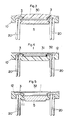
- a suitable encapsulating material 30 is filled on the carrier member 10 to hermetically seal the chip 1 and its electrical connection to the I/O pins 20 , as shown in FIG. 3 .
- the encapsulating material may be any conventional resins such as a silicon resin and epoxy resin.
- the chip 1 comprises a CCD (charged coupled device) or EPROM (erasable and programmable read-only-memory) requiring exposure to external light or ultraviolet light
- the encapsulation is made by a transparent material 31 , as shown in Fig. 4.
- a transparent plate 32 preferably made of glass is additionally placed over the transparent encapsulating material 31.
- Fig. 5 Another modification is shown in Fig. 5, in which only a transparent glass plate 32 is utilized to hermetically seal the chip 1 and its electrical connection to the I/O pins 20 within the package.
- the chip 1 and the wire elements 3 can be no longer restricted by the encapsulating material. This is effective in eliminating the possibility of chip crack or wire break which would be otherwise likely when the chip 1 and the wire elements 3 are in direct contact with the encapsulating material and subjected to thermal strain resulting from the difference in thermal coefficient of expansion between the encapsulating material and the chip 1 or wire elements 3. Further, the chip 1 and the wire elements 3 can be kept free from being attacked by corrosive impurities which may be present in the encapsulating material, improving the reliability of the package.
- the glass plate 32 has its periphery rested on stepped shoulder 12 in the top of the package and is secured thereat by a suitable adhesive or any other applicable bonding technique.
- the transparent plate 32 may be made of transparent resin material including epoxy resins.
- FIG. 6 shows a further modification of the above embodiment, in which the peripheral portion of the carrier member 10 is formed with outer and inner platforms 13 and 14 of different level.
- the I/O pins 20 in the outer and inner rows project respectively on the outer and inner platforms 13 and 14 so that the I/O pins 20 in the outer row have their top ends positioned in a level higher than those in the inner row. This contributes to improve the wireability since the wire elements 3 leading to the I/O pins 20 in the outer row can be vertically spaced from those leading to the I/O pins 20 in the inner row, as shown in the figure.
- FIG. 7 there is shown a second embodiment of the present invention which is characterized in that a plastic substrate 70 is utilized for electrical interconnection between a semiconductor chip 40 and a plurality of I/O pins 60.
- the I/O pins 60 which are molded in a carrier member 50 outwardly of a center recess 51 receiving the chip 40 , are likewise arranged on a pin grid as in the previous embodiment to have the staggered pin relation between the outer and inner rows.
- the I/O pins 60 have their top ends recessed from the top surface of the carrier member 50 so as to provide thereat a corresponding number of solder pits 55 , as show n in FIG. 8.
- the plastic substrate 70 is made from a thermosetting resin such as polyimide or glassfiber reinforced epoxy resin to be in the form of a thin plate or sheet having a center opening 71 smaller than the planar dimension of the chip 40.
- a trace pattern of conductor lines 72 as shown in Fig. 9, which extends from the outer periphery of the plastic substrate 70 and terminate in individual bonding lead 73 with a solder bump spaced evenly along the four sides of the center opening 71.
- Respectively formed in the conductor lines 72 at the peripheral portion of the plastic substrate 70 are another solder bumps 75 which are in registration with the solder pits 55 and the I/O pins 60.
- the plastic substrate 70 thus formed is placed over the carrier member 50 so that the solder bumps 75 of the conductor lines 72 fit into the respective solder pits 55 at the same time the bonding leads 73 thereof are in contact with the pads 41 of the chip 50. Subsequently, the package is subjected to reflow soldering for permanent joinder at the respective connections. Since the solder pits 55 receive the respective solder bumps 75 on the conductor lines 72, they serves to easily register the conductor lines 72 with the I/O pins 60 as well as with the pads 41 on the chip 45.
- the solder bumps 75 received therein undergo the melting within the confine thereof so as to be prevented from flowing over the top surface of the carrier member 50 and reaching the adjacent conductor lines 72, thus improving the wireability.
- the plastic substrate 70 itself is only secured at the soldering connections and is relatively free at the interface with the carrier member 50 so that it can well take up the thermal strain when there is a thermal mismatch between the materials forming the carrier member 50 and the plastic substrate 70.
- the plastic substrate 70 is made from the same thermosetting resin as the carrier member 50.
- the solder connection between the I/O pins 60 and the conductor lines 72 may be made by providing a solder in each of the solder pits 55 or on the top of the I/O pins 60 instead of forming the solder bumps 75 on the conductor lines 72.
- the package of this embodiment is sealed by a transparent plate 81 of glass or resin which is secured to the top of the carrier member 50 in spaced relation with the chip 40 and the plastic substrate 70 for the same purpose as described with reference to the package of FIG. 5.
- each of the I/O pins 60 has its top end flush with the top surface of the carrier member 50 and joined to each of the conductor lines 72 by means of a solder bump 75 formed on the conductor line 72. Additionally, the modification incorporates a heat sink 45 molded in the carrier member 50 for mounting thereon the chip 40.
- the other structures are identical to those in the embodiment of FIG. 7.
- FIG. 11 shows another form of the above modification in which the chip 40 and the plastic substrate 70 are encapsulated by a suitable encapsulating resin material 80.
- the I/O pins 60 are molded in the carrier member 50 with their top end projected above the top surface thereof for electrical connection with the corresponding conductor lines 72 of the plastic substrate 70.
- the staggered arrangement of the I/O pins are found to be equally or more effective for the pin grid array of more than two rows, and accordingly the present invention should be understood to include the pin grid array of more than two rows.
Landscapes
- Structures Or Materials For Encapsulating Or Coating Semiconductor Devices Or Solid State Devices (AREA)
Applications Claiming Priority (4)
| Application Number | Priority Date | Filing Date | Title |
|---|---|---|---|
| JP272191/86 | 1986-11-15 | ||
| JP61272190A JPS63126239A (ja) | 1986-11-15 | 1986-11-15 | ピングリツドアレイ |
| JP61272191A JPS63126253A (ja) | 1986-11-15 | 1986-11-15 | ピングリツドアレイ |
| JP272190/86 | 1986-11-15 |
Publications (2)
| Publication Number | Publication Date |
|---|---|
| EP0268181A1 true EP0268181A1 (fr) | 1988-05-25 |
| EP0268181B1 EP0268181B1 (fr) | 1992-07-29 |
Family
ID=26550077
Family Applications (1)
| Application Number | Title | Priority Date | Filing Date |
|---|---|---|---|
| EP87116524A Expired - Lifetime EP0268181B1 (fr) | 1986-11-15 | 1987-11-09 | Boîtier moulé en matière plastique avec grille de fiches pour dispositif à circuits intégrés |
Country Status (3)
| Country | Link |
|---|---|
| US (1) | US4868638A (fr) |
| EP (1) | EP0268181B1 (fr) |
| DE (1) | DE3780764T2 (fr) |
Cited By (5)
| Publication number | Priority date | Publication date | Assignee | Title |
|---|---|---|---|---|
| EP0232837A3 (en) * | 1986-02-14 | 1989-02-22 | Matsushita Electric Industrial Co., Ltd. | Plastic molded chip carrier package and method of fabricating the same |
| GB2251125A (en) * | 1990-12-20 | 1992-06-24 | Bosch Gmbh Robert | Making connections in electronic packages |
| EP0721212A1 (fr) * | 1989-11-29 | 1996-07-10 | Olin Corporation | Partie d'un boîtier électronique métallique |
| WO2003073502A1 (fr) * | 2002-02-26 | 2003-09-04 | Silicon Bandwidth, Inc. | Ensemble de reseau de micro-grille pour une matrice semi-conductrice |
| CN110364504A (zh) * | 2019-08-12 | 2019-10-22 | 昆山嘉华汽车电子科技有限公司 | 一种芯片模组及使用该芯片模组的电连接器 |
Families Citing this family (41)
| Publication number | Priority date | Publication date | Assignee | Title |
|---|---|---|---|---|
| US5917707A (en) | 1993-11-16 | 1999-06-29 | Formfactor, Inc. | Flexible contact structure with an electrically conductive shell |
| US5144412A (en) * | 1987-02-19 | 1992-09-01 | Olin Corporation | Process for manufacturing plastic pin grid arrays and the product produced thereby |
| US5108955A (en) * | 1988-10-27 | 1992-04-28 | Citizen Watch Co., Ltd. | Method of making a resin encapsulated pin grid array with integral heatsink |
| JPH0756887B2 (ja) * | 1988-04-04 | 1995-06-14 | 株式会社日立製作所 | 半導体パッケージ及びそれを用いたコンピュータ |
| JPH01313969A (ja) * | 1988-06-13 | 1989-12-19 | Hitachi Ltd | 半導体装置 |
| JP2772001B2 (ja) * | 1988-11-28 | 1998-07-02 | 株式会社日立製作所 | 半導体装置 |
| GB8918482D0 (en) * | 1989-08-14 | 1989-09-20 | Inmos Ltd | Packaging semiconductor chips |
| US4987478A (en) * | 1990-02-20 | 1991-01-22 | Unisys Corporation | Micro individual integrated circuit package |
| EP0463758A1 (fr) * | 1990-06-22 | 1992-01-02 | Digital Equipment Corporation | Empaquetage creux pour puce et procédé de fabrication |
| US6262477B1 (en) | 1993-03-19 | 2001-07-17 | Advanced Interconnect Technologies | Ball grid array electronic package |
| US5357672A (en) * | 1993-08-13 | 1994-10-25 | Lsi Logic Corporation | Method and system for fabricating IC packages from laminated boards and heat spreader |
| GB9320867D0 (en) * | 1993-10-11 | 1993-12-01 | Simpson Gareth | Adapter |
| US7073254B2 (en) | 1993-11-16 | 2006-07-11 | Formfactor, Inc. | Method for mounting a plurality of spring contact elements |
| US20020053734A1 (en) | 1993-11-16 | 2002-05-09 | Formfactor, Inc. | Probe card assembly and kit, and methods of making same |
| US5820014A (en) | 1993-11-16 | 1998-10-13 | Form Factor, Inc. | Solder preforms |
| US6177040B1 (en) * | 1993-11-24 | 2001-01-23 | Texas Instruments Incorporated | Method for making light transparent package for integrated circuit |
| US5458716A (en) * | 1994-05-25 | 1995-10-17 | Texas Instruments Incorporated | Methods for manufacturing a thermally enhanced molded cavity package having a parallel lid |
| US5550403A (en) * | 1994-06-02 | 1996-08-27 | Lsi Logic Corporation | Improved laminate package for an integrated circuit and integrated circuit having such a package |
| US5567984A (en) * | 1994-12-08 | 1996-10-22 | International Business Machines Corporation | Process for fabricating an electronic circuit package |
| US5866941A (en) * | 1995-02-23 | 1999-02-02 | Silicon Systems, Inc. | Ultra thin, leadless and molded surface mount integrated circuit package |
| US5994152A (en) | 1996-02-21 | 1999-11-30 | Formfactor, Inc. | Fabricating interconnects and tips using sacrificial substrates |
| US8033838B2 (en) | 1996-02-21 | 2011-10-11 | Formfactor, Inc. | Microelectronic contact structure |
| KR100186329B1 (ko) * | 1996-06-14 | 1999-03-20 | 문정환 | 고체 촬상 소자용 반도체 패키지 |
| US6281579B1 (en) * | 1997-02-14 | 2001-08-28 | International Rectifier Corporation | Insert-molded leadframe to optimize interface between powertrain and driver board |
| KR100479913B1 (ko) * | 1997-09-10 | 2005-06-16 | 삼성테크윈 주식회사 | 피지에이패키지 |
| JP3374732B2 (ja) * | 1997-11-17 | 2003-02-10 | 三菱電機株式会社 | 半導体素子モジュールおよび半導体装置 |
| JP3129275B2 (ja) * | 1998-02-27 | 2001-01-29 | 日本電気株式会社 | 半導体装置 |
| US6180045B1 (en) | 1998-05-20 | 2001-01-30 | Delco Electronics Corporation | Method of forming an overmolded electronic assembly |
| JP3602968B2 (ja) * | 1998-08-18 | 2004-12-15 | 沖電気工業株式会社 | 半導体装置およびその基板接続構造 |
| US6471525B1 (en) * | 2000-08-24 | 2002-10-29 | High Connection Density, Inc. | Shielded carrier for land grid array connectors and a process for fabricating same |
| JP2003229186A (ja) * | 2002-01-31 | 2003-08-15 | Denso Corp | 電子装置 |
| KR100457380B1 (ko) | 2002-05-06 | 2004-11-16 | 삼성전기주식회사 | 광마우스용 칩 온 보드 리드 패키지 및 그에 사용되는렌즈커버 |
| US7612443B1 (en) | 2003-09-04 | 2009-11-03 | University Of Notre Dame Du Lac | Inter-chip communication |
| US6972243B2 (en) * | 2003-09-30 | 2005-12-06 | International Business Machines Corporation | Fabrication of semiconductor dies with micro-pins and structures produced therewith |
| KR100634379B1 (ko) * | 2004-07-14 | 2006-10-16 | 삼성전자주식회사 | 반도체 패키지 |
| JP2011100718A (ja) * | 2009-10-05 | 2011-05-19 | Yazaki Corp | コネクタ |
| JP5599328B2 (ja) * | 2011-01-20 | 2014-10-01 | 三菱電機株式会社 | 電力用半導体装置とプリント配線板との接続機構 |
| US9620473B1 (en) | 2013-01-18 | 2017-04-11 | University Of Notre Dame Du Lac | Quilt packaging system with interdigitated interconnecting nodules for inter-chip alignment |
| US10658262B2 (en) * | 2018-02-27 | 2020-05-19 | Ball Aerospace & Technologies Corp. | Pin flexure array |
| US11094605B2 (en) | 2018-02-27 | 2021-08-17 | Ball Aerospace & Technologies Corp. | Systems and methods for supporting a component |
| US11410844B2 (en) * | 2019-09-13 | 2022-08-09 | Honeywell International Inc. | Enclosure for ion trapping device |
Citations (3)
| Publication number | Priority date | Publication date | Assignee | Title |
|---|---|---|---|---|
| EP0039160A2 (fr) * | 1980-04-29 | 1981-11-04 | Minnesota Mining And Manufacturing Company | Méthode pour assembler des bosses conductrices aux circuits électroniques |
| GB2136205A (en) * | 1983-03-09 | 1984-09-12 | Printed Circuits Int | Semiconductor chip carrier and contact array package and method of construction |
| US4618739A (en) * | 1985-05-20 | 1986-10-21 | General Electric Company | Plastic chip carrier package |
Family Cites Families (8)
| Publication number | Priority date | Publication date | Assignee | Title |
|---|---|---|---|---|
| US4326214A (en) * | 1976-11-01 | 1982-04-20 | National Semiconductor Corporation | Thermal shock resistant package having an ultraviolet light transmitting window for a semiconductor chip |
| US4338621A (en) * | 1980-02-04 | 1982-07-06 | Burroughs Corporation | Hermetic integrated circuit package for high density high power applications |
| JPS582054A (ja) * | 1981-06-26 | 1983-01-07 | Fujitsu Ltd | 半導体装置 |
| JPS59107551A (ja) * | 1982-12-13 | 1984-06-21 | Hitachi Ltd | 半導体装置 |
| JPS6055648A (ja) * | 1983-09-07 | 1985-03-30 | Toshiba Corp | 高密度実装基板 |
| JPS6150351A (ja) * | 1984-08-20 | 1986-03-12 | Oki Electric Ind Co Ltd | Eprom装置 |
| JPS61174752A (ja) * | 1985-01-30 | 1986-08-06 | Seiko Epson Corp | 半導体装置 |
| US4700473A (en) * | 1986-01-03 | 1987-10-20 | Motorola Inc. | Method of making an ultra high density pad array chip carrier |
-
1987
- 1987-11-09 EP EP87116524A patent/EP0268181B1/fr not_active Expired - Lifetime
- 1987-11-09 DE DE8787116524T patent/DE3780764T2/de not_active Expired - Lifetime
- 1987-11-13 US US07/121,506 patent/US4868638A/en not_active Expired - Fee Related
Patent Citations (3)
| Publication number | Priority date | Publication date | Assignee | Title |
|---|---|---|---|---|
| EP0039160A2 (fr) * | 1980-04-29 | 1981-11-04 | Minnesota Mining And Manufacturing Company | Méthode pour assembler des bosses conductrices aux circuits électroniques |
| GB2136205A (en) * | 1983-03-09 | 1984-09-12 | Printed Circuits Int | Semiconductor chip carrier and contact array package and method of construction |
| US4618739A (en) * | 1985-05-20 | 1986-10-21 | General Electric Company | Plastic chip carrier package |
Non-Patent Citations (5)
| Title |
|---|
| ELECTRONICS, 1977, pages 81-91, Technical articles: "Growing pin count is forcing LSI package changes" * |
| IBM TECHNICAL DISCLOSURE BULLETIN, vol. 21, no. 8, January 1979, page 3120; G.E. ANDRSON "Ceramic substrate with recessed pins" * |
| PATENT ABSTRACTS OF JAPAN, vol. 8, no. 226 (E-272)[1663], 17th Octobr 1984; & JP - A - 59 107 551 (HITACHI SEISAKUSHO K.K.) 21-06-1984 * |
| PATENT ABSTRACTS OF JAPAN, vol. 9, no. 185 (E-332)[1908], 31st July 1985; & JP - A - 60 55648 (TOSHIBA) 30-03-1985 * |
| SOLID STATE TECHNOLOGY, vol. 25, no. 6, June 1982, pages 94-100, New York, US; E.R. WINKLER "Integrated circuit packaging trends" * |
Cited By (8)
| Publication number | Priority date | Publication date | Assignee | Title |
|---|---|---|---|---|
| EP0232837A3 (en) * | 1986-02-14 | 1989-02-22 | Matsushita Electric Industrial Co., Ltd. | Plastic molded chip carrier package and method of fabricating the same |
| US4890152A (en) * | 1986-02-14 | 1989-12-26 | Matsushita Electric Works, Ltd. | Plastic molded chip carrier package and method of fabricating the same |
| EP0721212A1 (fr) * | 1989-11-29 | 1996-07-10 | Olin Corporation | Partie d'un boîtier électronique métallique |
| GB2251125A (en) * | 1990-12-20 | 1992-06-24 | Bosch Gmbh Robert | Making connections in electronic packages |
| GB2251125B (en) * | 1990-12-20 | 1995-02-22 | Bosch Gmbh Robert | Electronic component and method for its construction |
| WO2003073502A1 (fr) * | 2002-02-26 | 2003-09-04 | Silicon Bandwidth, Inc. | Ensemble de reseau de micro-grille pour une matrice semi-conductrice |
| US6734546B2 (en) | 2002-02-26 | 2004-05-11 | Silicon Bandwidth, Inc. | Micro grid array semiconductor die package |
| CN110364504A (zh) * | 2019-08-12 | 2019-10-22 | 昆山嘉华汽车电子科技有限公司 | 一种芯片模组及使用该芯片模组的电连接器 |
Also Published As
| Publication number | Publication date |
|---|---|
| DE3780764D1 (de) | 1992-09-03 |
| US4868638A (en) | 1989-09-19 |
| EP0268181B1 (fr) | 1992-07-29 |
| DE3780764T2 (de) | 1992-12-24 |
Similar Documents
| Publication | Publication Date | Title |
|---|---|---|
| US4868638A (en) | Plastic molded pin grid chip carrier package | |
| US5677575A (en) | Semiconductor package having semiconductor chip mounted on board in face-down relation | |
| US5262927A (en) | Partially-molded, PCB chip carrier package | |
| US6734557B2 (en) | Semiconductor device | |
| US5714800A (en) | Integrated circuit assembly having a stepped interposer and method | |
| US5557150A (en) | Overmolded semiconductor package | |
| US6660558B1 (en) | Semiconductor package with molded flash | |
| US6528869B1 (en) | Semiconductor package with molded substrate and recessed input/output terminals | |
| US6707140B1 (en) | Arrayable, scaleable, and stackable molded package configuration | |
| US5594626A (en) | Partially-molded, PCB chip carrier package for certain non-square die shapes | |
| US6531770B2 (en) | Electronic part unit attached to a circuit board and including a cover member covering the electronic part | |
| US6054774A (en) | Thin type semiconductor package | |
| US6798071B2 (en) | Semiconductor integrated circuit device | |
| US8330264B2 (en) | Packaging configurations for vertical electronic devices using conductive traces disposed on laminated board layers | |
| EP0729180A2 (fr) | Empaquetage de modules à multi-puces sans interconnexion à fil | |
| EP0435093A2 (fr) | Dispositif électronique moulé, mince pour le montage en surface | |
| US5708304A (en) | Semiconductor device | |
| JPH08111433A (ja) | 半導体装置及び半導体装置製造用テープ | |
| EP0670594A1 (fr) | Empaquetage pour semi-conducteur et procédé de fabrication | |
| JP2895022B2 (ja) | チップスケールパッケージの製造方法 | |
| KR100226335B1 (ko) | 플라스틱 성형회로 패키지 | |
| US5849609A (en) | Semiconductor package and a method of manufacturing thereof | |
| US6437430B2 (en) | Semiconductor apparatus and frame used for fabricating the same | |
| KR100279252B1 (ko) | 세라믹패키지 | |
| JP2993480B2 (ja) | 半導体装置 |
Legal Events
| Date | Code | Title | Description |
|---|---|---|---|
| PUAI | Public reference made under article 153(3) epc to a published international application that has entered the european phase |
Free format text: ORIGINAL CODE: 0009012 |
|
| AK | Designated contracting states |
Kind code of ref document: A1 Designated state(s): DE FR GB |
|
| 17P | Request for examination filed |
Effective date: 19880822 |
|
| 17Q | First examination report despatched |
Effective date: 19910510 |
|
| GRAA | (expected) grant |
Free format text: ORIGINAL CODE: 0009210 |
|
| AK | Designated contracting states |
Kind code of ref document: B1 Designated state(s): DE FR GB |
|
| REF | Corresponds to: |
Ref document number: 3780764 Country of ref document: DE Date of ref document: 19920903 |
|
| ET | Fr: translation filed | ||
| PLBE | No opposition filed within time limit |
Free format text: ORIGINAL CODE: 0009261 |
|
| STAA | Information on the status of an ep patent application or granted ep patent |
Free format text: STATUS: NO OPPOSITION FILED WITHIN TIME LIMIT |
|
| 26N | No opposition filed | ||
| PGFP | Annual fee paid to national office [announced via postgrant information from national office to epo] |
Ref country code: GB Payment date: 19931101 Year of fee payment: 7 |
|
| PGFP | Annual fee paid to national office [announced via postgrant information from national office to epo] |
Ref country code: FR Payment date: 19931110 Year of fee payment: 7 Ref country code: DE Payment date: 19931110 Year of fee payment: 7 |
|
| PG25 | Lapsed in a contracting state [announced via postgrant information from national office to epo] |
Ref country code: GB Effective date: 19941109 |
|
| GBPC | Gb: european patent ceased through non-payment of renewal fee |
Effective date: 19941109 |
|
| PG25 | Lapsed in a contracting state [announced via postgrant information from national office to epo] |
Ref country code: FR Effective date: 19950731 |
|
| PG25 | Lapsed in a contracting state [announced via postgrant information from national office to epo] |
Ref country code: DE Effective date: 19950801 |
|
| REG | Reference to a national code |
Ref country code: FR Ref legal event code: ST |