EP0269185A2 - Dispositif de commutation à hystérèse dynamique - Google Patents
Dispositif de commutation à hystérèse dynamique Download PDFInfo
- Publication number
- EP0269185A2 EP0269185A2 EP87202299A EP87202299A EP0269185A2 EP 0269185 A2 EP0269185 A2 EP 0269185A2 EP 87202299 A EP87202299 A EP 87202299A EP 87202299 A EP87202299 A EP 87202299A EP 0269185 A2 EP0269185 A2 EP 0269185A2
- Authority
- EP
- European Patent Office
- Prior art keywords
- inverter
- transistor
- voltage
- fet
- integrated circuit
- Prior art date
- Legal status (The legal status is an assumption and is not a legal conclusion. Google has not performed a legal analysis and makes no representation as to the accuracy of the status listed.)
- Granted
Links
Images


Classifications
-
- H—ELECTRICITY
- H03—ELECTRONIC CIRCUITRY
- H03K—PULSE TECHNIQUE
- H03K17/00—Electronic switching or gating, i.e. not by contact-making and –breaking
- H03K17/51—Electronic switching or gating, i.e. not by contact-making and –breaking characterised by the components used
- H03K17/56—Electronic switching or gating, i.e. not by contact-making and –breaking characterised by the components used by the use, as active elements, of semiconductor devices
- H03K17/687—Electronic switching or gating, i.e. not by contact-making and –breaking characterised by the components used by the use, as active elements, of semiconductor devices the devices being field-effect transistors
-
- H—ELECTRICITY
- H03—ELECTRONIC CIRCUITRY
- H03K—PULSE TECHNIQUE
- H03K3/00—Circuits for generating electric pulses; Monostable, bistable or multistable circuits
- H03K3/02—Generators characterised by the type of circuit or by the means used for producing pulses
- H03K3/353—Generators characterised by the type of circuit or by the means used for producing pulses by the use, as active elements, of field-effect transistors with internal or external positive feedback
- H03K3/356—Bistable circuits
- H03K3/3565—Bistables with hysteresis, e.g. Schmitt trigger
-
- H—ELECTRICITY
- H03—ELECTRONIC CIRCUITRY
- H03K—PULSE TECHNIQUE
- H03K19/00—Logic circuits, i.e. having at least two inputs acting on one output; Inverting circuits
- H03K19/003—Modifications for increasing the reliability for protection
- H03K19/00346—Modifications for eliminating interference or parasitic voltages or currents
- H03K19/00361—Modifications for eliminating interference or parasitic voltages or currents in field effect transistor circuits
Definitions
- This invention relates to switching devices suitable for seminconductor applications.
- FIG. 1 illustrates a portion of a digital IC 10 that receives largely constant external supply voltages V HH and V LL at respective externally accessible supply terminal (or pads) T H and T L .
- V HH is greater than V LL .
- IC 10 produces a circuit output voltage V O at an externally accessible output terminal T O in response to a circuit input voltage V I received at an externally accessible input terminal T I .
- a capacitor C O which may be real or parasitic, is connected between terminal T O and the V LL supply.
- the illustrated portion of IC 10 is a conventional inverting driver powered by high and low internal supply voltages V H and V L provided on lines connected respectively to terminals T H and T L . Responsive to an internal input voltage V A supplied on a line connected to terminal T I , the driver produces an internal output voltage V D on a line connected to terminal T O . Parasitic inductances L L , L H , L I and L O are respectively associated with the lines carrying voltages V L , V H , V A and V D .
- the driver consists of an input inverter 12, an intermediate inverter 14, and an output inverter 16, each of which is progressively larger so as to provide progressively more current.
- Inverter 12 is formed with complementary input field-effect transistors (FET's) Q1 N and Q1 P whose gates receive voltage V A and whose interconnected drains provide an inverter output voltage V B logically inverse to voltage V A .
- Inverter 16 consists of complementary output FET's Q2 N and Q2 P whose gates receive voltage V C and whose interconnected drains provide voltage V D as the inverse of voltage V C .
- FET's Q1 N and Q2 N are N-channel devices whose sources are connected to the V L supply line.
- FET's Q1 P and Q2 P are P-channel transistors having their sources tied to the V H supply line.
- inverter 12 changes state as the voltage difference V A -V L passes an inverter threshold voltage V T .
- Threshold V T is at a nominal value V S when internal supply voltages V L and V H are respectively at (or very close to) V LL and V HH .
- inverter 12 switches from a high logic state to a low logic state as voltage V A rises above V LL + V S .
- voltage V B which goes from a high voltage level close to V HH to a low voltage level close to V LL .
- V A later drops below V LL +V S inverter 12 switches from its low logic state to its high logic state.
- V B then rises from V LL back up to V HH .
- V I changes very slowly.
- V I is initially low.
- V L and V H are respectively at V LL and V HH .
- V A is then low, causing V B to be at V HH .
- V C is low so that FET Q2 N is turned off and FET Q2 P is turned on.
- V D and V O are both at V HH .
- Capacitor C O is charged to a high level.
- V A tracks V I closely. Inductance L I does not have any significant effect on V A .
- V A starts to go above V LL +V S . This causes V B to drop rapidly to V LL .
- V C goes high to turn FET Q2 N on and FET Q2 P off.
- V D drops rapidly to V LL .
- capacitor C O starts discharging to the V LL supply by way of a path through elements L O , Q2 N and L L to pull V O rapidly down to V LL .
- the current flowing through this path varies with time in a non-linear manner. Since the voltage across an inductor is the inductance times the time rate of change of current flowing through the inductor, a positive voltage builds up across inductance L L , reaching a maximum, at a time t3. A positive (or upward going) spike in V L thereby occurs at t3 as shown in Fig. 2.
- the V L spike at t3 is the "first" spike in a set of timewise contiguous pairs of alternating spikes that die out quickly, of which only the first pair of alternating spikes are actually shown in Fig. 2. The same applies to the further supply line spikes discussed below for Fig. 2 and to the supply line spikes illustrated in the other time diagrams herein.
- V L spike at t3 is often so high that V A -V L temporarily drops below threshold V T . This is true even though the attendant reduction of the difference between V H and V L during the positive V L spike reduces V T somewhat. See shaded area 18 in Fig. 2. (Note that the comparison of V L to V A -V T shown in the various time diagrams herein is equivalent to the comparison of V A -V L to V T which is more difficult to illustrate graphically).
- Inverter 12 then makes a pair of rapid changes in logic state at approximately a time t4, causing V B to spike upwards. In turn, the V B spike causes a positive V O spike to occur at a time t5. Even if the C O discharge current flowing through FET Q2 N in output inverter 16 were not sufficient in itself to cause the V O spike, it could be produced as the result of several such output inverters acting in unison in IC 10.
- V I drops slowly, except that the polarities and supply lines are reversed.
- the first spike is a negative V H spike that results from the rapid charging of capacitor C O by way of a path through elements L H , Q2 P and L O .
- V O spikes and the corresponding spikes in V B , V C and V D can be disastrous. They can cause a circuit (such as a flip-flop) responsive to V O , V B , V C or V D to be set in a wrong state.
- a circuit such as a flip-flop
- inverter 12 With a device (such as a Schmitt trigger) having a pair of separate static voltage thresholds. While static hysteresis might be useful in certain applications, it is not effective if the two thresholds must lie within a narrow voltage range. A solution that entails a single static threshold is desirable.
- a switching device utilizes dynamic hysteresis to prevent internal supply line voltage bounce from causing unwanted changes in state.
- the present hysteresis is termined "dynamic" because a change in device threshold voltage triggered by a change in logic state occurs only for a prescribed period of time. When that period expires, the threshold voltage automatically returns to its original value.
- the device therefore has only one static threshold. This makes the invention especially useful in a high-speed IC having a narrow threshold range in which the input voltage must switch.
- the invention also avoids the additional propagation delays that normally occur with static hysteresis.
- the present device is incorporated in an electronic circuit in which a low supply voltage V L and a high supply voltage V H are provided to power the device.
- the device changes state as V A -V L passes a threshold voltage V T .
- threshold V T substantially at a value V S
- voltages V L and V H substantially at respective values V LL and V HH
- the device switches from a first state to a second state as V A rises above V LL +V S and from the second state to the first state as V A drops below V LL +V S .
- the device includes a dynamic hysteresis circuit that, after V A rises above V LL +V S , temporarily decreases V T below that which would otherwise be present and/or, after V A drops below V LL +V S , temporarily increases V T above what would otherwise be present.
- V T normally returns to V S before V A starts moving in the direction opposite to that in which it was moving when V T changed.
- the device typically contains a pair of input N-channel and P-channel FET's having gates responsive to voltage V A , sources respectively coupled to the lines carrying voltages V L and V H , and drains coupled together to provide an output voltage V B inverse to voltage V A .
- the hysteresis circuit performs both of the above operations on threshold V T , the hysteresis circuit is preferably formed with a control circuit and a pair of further N-channel and P-channel FET's having gates responsive to signals from the control circuit. sources respectively coupled to the V L and V H lines, and drains coupled to the drains of the input FET's.
- the control circuit causes the further N-channel FET to turn on temporarily in response to voltage V B going from a high level to a low level. This temporarily increases the width of the pertinent conducting N-channel area in the device so as to reduce V T until the further N-channel FET turns off. Likewise, the control circuit causes the further P-channel FET to turn on temporarily in response to voltage V B going from its low level to its high level. The width of the pertinent conducting P-channel area in the device thereby increases to raise V T briefly.
- V T The temporary change in V T provides a clearance that prevents the present device from making a pair of rapid changes of state as a result of internal supply line bounce when V A is changing slowly. This avoids output voltage spikes.
- each N-channel FET has an arrow pointing towards its channel.
- Each P-channel FET has an arrow pointing away from its channel. All of the FET's shown in the drawings are enhancement-mode insulated-gate devices.
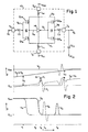
- Fig. 3 illustrates a portion of a digital IC 20 in which a very fast logic circuit powered by high and low internal supply voltages V H and V L operates on input voltage V A and possibly on other input voltages (not shown) to produce output voltage V D .
- the logic circuit contains an input inverting device 22 that produces voltage V B as the logical inverse of voltage V A .
- Device 22 is formed with input inverter 12 consisting of FET's Q1 N and Q1 P arranged as described above and a circuit 24 that provides dynamic hysteresis for the threshold voltage V T of device 22.
- Dynamic hysteresis circuit 24 consists of a control circuit 26 powered by supply voltages V H and V L , an N-channel FET Q3 N , and a P-channel FET Q3 P .
- control circuit 26 supplies threshold-control voltages V N and V P to the respective gates of FET's Q3 N and Q3 P .
- Their sources are respectively connected to the V L and V H supply lines, while their drains are connected to the drains of FET's Q1 N and Q1 P to produce voltage V B .
- FET Q3 N is therefore "in parallel" with FET Q1 N .
- FET's Q3 P and Q1 P are in parallel.
- the threshold voltage for an inverter formed with complementary FET's depends on the ratio R P/N of the P-channel width to the N-channel width (at constant channel length). This means the widths of the channel areas that are conducting at the threshold point. The threshold voltage increases when R P/N increases and vice versa.
- the quiescent value of R P/N for device 22 is simply the Q1 P channel width divided by the Q1 N channel width since FET's Q1 N and Q1 P are both conducting at the threshold point, one in the midst of turning on and the other in the midst of turning off. If FET Q3 N is on but FET Q3 P is off, the N-channel width for device 22 increases since FET's Q3 N and Q1 N are in parallel. R P/N for device 22 is therefor less than its quiescent value. In like manner, R P/N for device 22 is greater than the quiescent value when FET Q3 P is on but FET Q3 N is off.
- device 22 operates as follows. FET's Q3 N and Q3 P are initially off. Supply voltages V L and V H are initially at (or very near) respective substantially constant levels V LL and V HH . Under these conditions, threshold V T is at quiescent value V S determined by the quiescent R P/N of device 22. When V A -V L passes V T , device 22 changes state.
- V A rises above V LL +V S , FET Q1 N turns on and FET Q1 P turns off.
- Device 22 as manifested by the conductive conditions of FET's Q1 N and Q1 P switches from a high logic state to a low logic state, causing voltage V B to go from a high level near V HH to a low level near V LL .
- control circuit 26 temporarily raises V N enough to turn FET Q3 N on for a brief period.
- FET Q3 P remains off.
- R P/N drops below its quiescent level. This reduces V T until circuit 26 reduces V N sufficiently to turn FET Q3 N back off.
- V A drops below V LL +V S .
- FET Q1 N turns off and FET Q1 P turns on, causing device 22 to switch from its low logic state to its high logic state.
- V B goes from V LL up to V HH .
- circuit 26 temporarily provides V P at a sufficiently low voltage to turn FET Q3 P on for a short time.
- FET Q3 N stays off. Consequently, R P/N rises above its quiescent value so as to increase V T .
- V T drops back down.
- the logic circuit in IC 20 also contains an intermediate logic section 28 and output inverter 16.
- Logic section 28 may perform any of a number of logical functions such as inversion, ANDing, and ORing. Section 28 might also be a non-inverting buffer or simply a direct connection. Depending on how section 28 is configured, it operates on voltage V B and possibly on other input voltages (not shown) to produce voltage V C at a value that is logically the same as or inverse to voltage V B .
- Inverter 16 consists of FET's Q2 N and Q2 P arranged as described above to produce voltage V D as the inverse of voltage V C .
- Circuit input voltage V I and external supply voltages V LL and V HH are supplied respectively to externally accessible terminals T I , T L and T H which are interconnected with the logic circuit via parasitic inductances L I , L L and L H in IC 20 in the same way that these elements are interconnected with the inverting driver in IC 10.
- FIG. 4a is a pair of simplified diagrams illustrating voltage variation as a function of time for IC 20 for the case in which V I rises slowly.
- Fig. 4b is a corresponding pair of simplified time diagrams for the situation in which V I falls slowly.
- V L is initially at V LL while V H is initially at V HH .
- Threshold V T thus starts at V S .
- Fig, 4a which is analogous to Fig. 2.
- V I , V A , V B and V O are initially at the values given above for Fig. 2.
- Capacitor C O is charged to a high level.
- Inductance L I again has no singificant effect.
- V A passes V LL +V S at time t1
- V B drops rapidly to V LL .
- hysteresis circuit 24 reduces V T starting at a time t 1.5 .
- the difference between dotted line 30 and the solid line representing V A -V T in Fig. 4a indicates the amount of reduction in V T .
- Capacitor C O starts discharging at time t2. This produces a positive V L spike at time t3 according to the mechanism described above for IC 10. The attendant reduction of the difference between V H and V L at t3 does result in a further V T reduction beyond that already caused by circuit 24. However, due solely to the V T reduction produced by circuit 24, V A -V L stays above V T during the positive V L spike. Capacitor C O thereby remains discharged so as to substantially inhibit any further internal supply line voltage bounce. Accordingly, no spikes occur in V B , V C , V D and V O .
- V T automatically returns to V S .
- the circuit timing parameters and device values are preferably chosen in such a manner that V T goes back to V S before V I and V A start to drop in subsequent switching operation.
- the falling V I situation of Fig. 4b is essentially the complement of that of Fig. 4a.
- hysteresis circuit 24 increases V T between t 1.5 and t 3.5 .
- the amount of V T increase is indicated by the difference between dotted line 32 and the solid line labeled V A -V T .
- V A -V L remains below V T during the negative V H spike to prevent further spiking.
- section 28 might generate V C at the same logical value as V B . If V I rises slowly, the first supply line spiking occurs on the V H line as a negative spike followed immediately by a positive spike. Circuit 24 decreases V T to prevent V A -V L from dropping below V T during the positive V H spike -- i.e., the second spike in the pair of alternating V H spikes. The same applies when V I drops slowly except that the polarities and supply lines are reversed. Since the magnitude of the second spike in each pair of alternating internal supply line spikes is normally slightly less than the magnitude of the first spike, the situation in which V C and V B are logically the same is not as critical as when V C is the inverse of V B .
- Circuit 26 here consists of complementary charge-supply FET's Q4 N and Q4 P , capacitors C1 and C2, and complementary discharge FET's Q5 N and Q5 P connected as shown in Fig. 5.
- FET's Q4 N and Q4 P are arranged as an inverter 34 with their drains connected together to provide a voltage V E inverse to voltage V B supplied to their gates.
- Circuit 26 in Fig. 5 operates in the following way.
- V B drops from V HH to V LL
- FET Q4 N turns off and FET Q4 P turns on.
- Current from the V H line flows through FET Q4 P to capacitors C1 and C2.
- Capacitor C1 provides positive charge to the Q3 N gate for a short period of time. During this period, charge also flows to the V L line by way of a path through FET Q5 N which turns on.
- a competition thus exists between the charging of the Q3 N gate by capacitor C1 and the discharging of the Q3 N gate through FET Q5 N .
- the average charge rate during the charging period exceeds the average discharge rate by an amount sufficiently great so that voltage V N rises enough to turn FET Q3 N on. Shortly afterwards, the charge on the Q3 N gate dissipates sufficiently through FET Q5 N to cause FET Q3 N to turn back off.
- V B returns to V HH at a later time, elements Q4 N , C2 and Q5 P function in a complementary manner to enable FET Q3 P to turn on briefly.
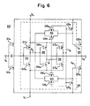
- circuit 26 consists of inverter 34, an inverter 36 that inverts voltage V E to produce a voltage V F , an inverter 38 that inverts voltage V F to produce a voltage V G , transmission gates 40 and 42, and discharge FET's Q5 N and Q5 P whose gates receive voltage V G here.
- FET Q5 N is source-drain connected between the V L line and the Q3 N gate.
- FET Q5 P is similarly source-drain connected between the V H line and the Q3 P gate.
- Inverter 36 consists of complementary FET's Q6 N and Q6 P arranged in the conventional manner shown.
- inverter 38 consists of FET's Q7 N and Q7 P connected conventionally.
- Gate 40 is formed with complementary FET's Q8 N and Q8 P whose gates respectively receive voltages V F and V G .
- FET's Q8 N and Q8 P have interconnected first source/drain elements connected to the Q4 N and Q4 P drains and interconnected second source/drain elements connected to the Q3 N gate.
- Gate 42 consists of complementary FET's Q9 N and Q9 P aranged with regard to the Q3 P gate in a manner that is complementary to the arrangement of gate 40 with respect to the Q3 N gate.
- Circuit 26 in Fig. 6 operates as follows. Assume that V B is initially at V HH so that FET Q4 N is on and FET Q4 P is off. V F is likewise at V HH . V E and V G are both at V LL . FET Q8 N is on, thereby setting V N at V LL . FET's Q3 N , Q5 N and Q8 P are all off. When V B drops to V LL , FET Q4 N turns off and FET Q4 P turns on. V E rises to V HH . During an initial part of the time needed for inverter 36 to drop V F down to V LL , positive charge form the V H line flows through FET's Q4 P and Q8 N to the Q3 N gate.
- V N increases, enabling FET Q8 P to turn on.
- FET Q8 N gradually turns off, positive charge from the V H line now flows through FET's Q4 P and Q8 P to the Q3 N gate to raise V N further. This continues for the entire time needed for inverter 36 to raise V G up to V HH . At some point during the charging of the Q3 N gate, FET Q3 N turns on.
- FET Q8 P turns off to stop the charging of the Q3 N gate.
- FET Q5 N turns on. It opens a path to the V L line for discharging the Q3 N gate, causing FET Q3 N to turn off.
- Inverters 36 and 38 and FET's Q4 N , Q9 N , Q9 P and Q5 P operate in a similar, complementary manner to enable FET Q3 P to turn on briefly when V B later returns to V HH .
- a delay element can be placed in series with inverter 36 or 38.
- the delay element might, for example, consist of a pair of inverters in series.
- V LL and V HH preferably are 0 volt (ground) and 5 volts.
- FET's Q1 N , Q1 P , Q3 N , Q3 P , Q4 N , Q4 P , Q5 N , Q5 P , Q6 N /Q7 N , Q6 P /Q7 P , Q8 N /Q9 N , and Q8 P /Q9 P have respective channel widths of 100, 270, 50, 100, 20, 50, 1, 5, 5, 10, 10 and 25 microns.
- the channel length for all of these FET's is preferably 1 micron except for FET Q5 N whose channel length is 5 microns.
- V A the values at which V A is provided from an IC preceding IC 20 may not be appropriate for driving FET's Q1 N and Q1 P directly with V A so as to achieve a desired quiescent (V S ) value for V T .
- V S quiescent
- Such cases can be handled by inserting a non-inverting buffer in the line leading to the gate of one of FET's Q1 N and Q1 P .
- the buffer might, for example consist of a pair of inverters in series. Nonetheless, the gates of FET's Q1 N and Q1 P are still responsive to V A .
- Such an arrangement does not have any particularly significant effect on the dynamic hysteresis.
- junction FET's could be used instead of insulated-gate FET's.
- Certain of the enhancement-mode FET's could be replaced with depletion-mode FET's. If dynamic hysteresis is needed only when input V I rises, FET Q3 P and the portions of circuit 26 not used with FET Q3 N (for example, FET's Q5 P , Q9 N and Q9 P in Fig. 6) could be deleted. The converse applies if dynamic hysteresis is needed only when V I falls.
- threshold V T was defined with respect to low supply voltage V L merely because this is the normal convention.
- V T could as well have been defined with reference to high supply voltage V H without changing the design, physical operation, or effect of the invention. The only difference is that the polarities relating to V T would generally have to be reversed in the operational explanation.
Landscapes
- Physics & Mathematics (AREA)
- Engineering & Computer Science (AREA)
- Computer Hardware Design (AREA)
- Computing Systems (AREA)
- General Engineering & Computer Science (AREA)
- Mathematical Physics (AREA)
- Logic Circuits (AREA)
- Electronic Switches (AREA)
Applications Claiming Priority (2)
| Application Number | Priority Date | Filing Date | Title |
|---|---|---|---|
| US06/934,753 US4740717A (en) | 1986-11-25 | 1986-11-25 | Switching device with dynamic hysteresis |
| US934753 | 1986-11-25 |
Publications (3)
| Publication Number | Publication Date |
|---|---|
| EP0269185A2 true EP0269185A2 (fr) | 1988-06-01 |
| EP0269185A3 EP0269185A3 (en) | 1989-10-18 |
| EP0269185B1 EP0269185B1 (fr) | 1994-08-31 |
Family
ID=25466004
Family Applications (1)
| Application Number | Title | Priority Date | Filing Date |
|---|---|---|---|
| EP87202299A Expired - Lifetime EP0269185B1 (fr) | 1986-11-25 | 1987-11-24 | Dispositif de commutation à hystérèse dynamique |
Country Status (6)
| Country | Link |
|---|---|
| US (2) | US4740717A (fr) |
| EP (1) | EP0269185B1 (fr) |
| JP (1) | JPH07118635B2 (fr) |
| KR (1) | KR950008422B1 (fr) |
| DE (1) | DE3750463T2 (fr) |
| HK (1) | HK60796A (fr) |
Cited By (1)
| Publication number | Priority date | Publication date | Assignee | Title |
|---|---|---|---|---|
| FR2649265A1 (fr) * | 1989-06-30 | 1991-01-04 | Standard Microsyst Smc | Circuit amplificateur-separateur pour la conversion ttl-cmos |
Families Citing this family (30)
| Publication number | Priority date | Publication date | Assignee | Title |
|---|---|---|---|---|
| JPS63234623A (ja) * | 1987-03-23 | 1988-09-29 | Toshiba Corp | 半導体集積回路 |
| US4947063A (en) * | 1987-10-09 | 1990-08-07 | Western Digital Corporation | Method and apparatus for reducing transient noise in integrated circuits |
| JPH01113993A (ja) * | 1987-10-28 | 1989-05-02 | Toshiba Corp | 半導体集積回路 |
| US5182479A (en) * | 1988-06-24 | 1993-01-26 | U.S. Philips Corp. | Gate circuit having increased voltage handling capability |
| EP0369055A1 (fr) * | 1988-11-17 | 1990-05-23 | Siemens Aktiengesellschaft | Circuit de compensation des signaux de bruit |
| JPH0666674B2 (ja) * | 1988-11-21 | 1994-08-24 | 株式会社東芝 | 半導体集積回路の出力回路 |
| US4989127A (en) * | 1989-05-09 | 1991-01-29 | North American Philips Corporation | Driver for high voltage half-bridge circuits |
| US4967109A (en) * | 1989-12-08 | 1990-10-30 | General Electric Company | High efficiency gate driver circuit for a high frequency converter |
| JP2671538B2 (ja) * | 1990-01-17 | 1997-10-29 | 松下電器産業株式会社 | 入力バッファ回路 |
| US5049764A (en) * | 1990-01-25 | 1991-09-17 | North American Philips Corporation, Signetics Div. | Active bypass for inhibiting high-frequency supply voltage variations in integrated circuits |
| EP0466238A3 (en) * | 1990-07-06 | 1992-02-26 | N.V. Philips' Gloeilampenfabrieken | Driver circuit |
| WO1992016998A1 (fr) | 1991-03-18 | 1992-10-01 | Quality Semiconductor, Inc. | Commutateur a grille de transmission rapide |
| US6208195B1 (en) | 1991-03-18 | 2001-03-27 | Integrated Device Technology, Inc. | Fast transmission gate switch |
| US5194768A (en) * | 1992-03-27 | 1993-03-16 | Advanced Micro Devices, Inc. | Apparatus for filtering noise from a periodic signal |
| US5332938A (en) * | 1992-04-06 | 1994-07-26 | Regents Of The University Of California | High voltage MOSFET switching circuit |
| US5296766A (en) * | 1992-06-04 | 1994-03-22 | Sharp Microelectronics Technology, Inc. | CMOS circuit with crowbar limiting function |
| US5373435A (en) * | 1993-05-07 | 1994-12-13 | Philips Electronics North America Corporation | High voltage integrated circuit driver for half-bridge circuit employing a bootstrap diode emulator |
| US5666280A (en) * | 1993-05-07 | 1997-09-09 | Philips Electronics North America Corporation | High voltage integrated circuit driver for half-bridge circuit employing a jet to emulate a bootstrap diode |
| US5502632A (en) * | 1993-05-07 | 1996-03-26 | Philips Electronics North America Corporation | High voltage integrated circuit driver for half-bridge circuit employing a bootstrap diode emulator |
| US5386153A (en) * | 1993-09-23 | 1995-01-31 | Cypress Semiconductor Corporation | Buffer with pseudo-ground hysteresis |
| US5532617A (en) * | 1994-03-25 | 1996-07-02 | Philips Electronics North America Corporation | CMOS input with temperature and VCC compensated threshold |
| JPH088709A (ja) * | 1994-06-17 | 1996-01-12 | Harris Corp | ブリッジ制御回路 |
| US6166982A (en) * | 1998-06-25 | 2000-12-26 | Cypress Semiconductor Corp. | High voltage switch for eeprom/flash memories |
| US6294959B1 (en) | 1999-11-12 | 2001-09-25 | Macmillan Bruce E. | Circuit that operates in a manner substantially complementary to an amplifying device included therein and apparatus incorporating same |
| US6281736B1 (en) | 1999-12-02 | 2001-08-28 | Sun Microsystems, Inc. | Method and circuitry for soft fuse row redundancy with simple fuse programming |
| DE10158112C1 (de) * | 2001-11-27 | 2003-06-26 | Texas Instruments Deutschland | Ausgangstreiberschaltung |
| KR100532477B1 (ko) * | 2003-10-24 | 2005-12-01 | 삼성전자주식회사 | 입력 신호의 트랜지션 구간에서 안정적으로 동작하는 패스게이트 회로와 이를 구비하는 셀프 리프레쉬 회로 및 패스게이트 회로의 제어방법 |
| US20080290841A1 (en) * | 2007-05-23 | 2008-11-27 | Richtek Technology Corporation | Charging Circuit for Bootstrap Capacitor and Integrated Driver Circuit Using Same |
| JP5431992B2 (ja) * | 2010-02-09 | 2014-03-05 | セイコーインスツル株式会社 | トランスミッションゲート及び半導体装置 |
| WO2025091091A1 (fr) * | 2023-11-03 | 2025-05-08 | Nexalist Pty Ltd | Système et procédé de commande d'erreur d'hystérésis dynamique à cycle unique |
Family Cites Families (10)
| Publication number | Priority date | Publication date | Assignee | Title |
|---|---|---|---|---|
| US3718864A (en) * | 1971-02-26 | 1973-02-27 | Cogar Corp | Crossover detector |
| US4039858A (en) * | 1976-04-05 | 1977-08-02 | Rca Corporation | Transition detector |
| DE2901340A1 (de) * | 1979-01-15 | 1980-07-24 | Vdo Schindling | Schaltungsanordnung zur erzeugung einer rechteckspannung |
| JPS58182914A (ja) * | 1982-04-21 | 1983-10-26 | Hitachi Ltd | Cmosヒステリシス回路 |
| US4498021A (en) * | 1982-07-13 | 1985-02-05 | Matsushita Electric Industrial Co., Ltd. | Booster for transmitting digital signal |
| JPS5949020A (ja) * | 1982-09-13 | 1984-03-21 | Toshiba Corp | 論理回路 |
| US4507570A (en) * | 1983-03-01 | 1985-03-26 | Motorola, Inc. | Resettable one shot circuit having noise rejection |
| US4532436A (en) * | 1983-09-30 | 1985-07-30 | Rca Corporation | Fast switching circuit |
| GB8420651D0 (en) * | 1984-08-14 | 1984-09-19 | British Telecomm | Interface circuit |
| US4609834A (en) * | 1984-12-24 | 1986-09-02 | Burroughs Corporation | Integrated logic circuit incorporating a module which generates a control signal that cancels switching noise |
-
1986
- 1986-11-25 US US06/934,753 patent/US4740717A/en not_active Expired - Lifetime
-
1987
- 1987-11-24 JP JP62295921A patent/JPH07118635B2/ja not_active Expired - Lifetime
- 1987-11-24 DE DE3750463T patent/DE3750463T2/de not_active Expired - Fee Related
- 1987-11-24 KR KR1019870013214A patent/KR950008422B1/ko not_active Expired - Fee Related
- 1987-11-24 EP EP87202299A patent/EP0269185B1/fr not_active Expired - Lifetime
-
1988
- 1988-04-08 US US07/180,425 patent/US4874971A/en not_active Expired - Fee Related
-
1996
- 1996-04-11 HK HK60796A patent/HK60796A/en not_active IP Right Cessation
Cited By (1)
| Publication number | Priority date | Publication date | Assignee | Title |
|---|---|---|---|---|
| FR2649265A1 (fr) * | 1989-06-30 | 1991-01-04 | Standard Microsyst Smc | Circuit amplificateur-separateur pour la conversion ttl-cmos |
Also Published As
| Publication number | Publication date |
|---|---|
| US4740717A (en) | 1988-04-26 |
| DE3750463D1 (de) | 1994-10-06 |
| KR950008422B1 (ko) | 1995-07-28 |
| EP0269185A3 (en) | 1989-10-18 |
| JPH07118635B2 (ja) | 1995-12-18 |
| JPS63172513A (ja) | 1988-07-16 |
| EP0269185B1 (fr) | 1994-08-31 |
| KR880006848A (ko) | 1988-07-25 |
| HK60796A (en) | 1996-04-19 |
| DE3750463T2 (de) | 1995-04-13 |
| US4874971A (en) | 1989-10-17 |
Similar Documents
| Publication | Publication Date | Title |
|---|---|---|
| EP0269185B1 (fr) | Dispositif de commutation à hystérèse dynamique | |
| EP0329285B1 (fr) | Tampon de sortie | |
| EP0212584B1 (fr) | Circuit de sortie avec stabilisation du niveau | |
| US5034629A (en) | Output control circuit for reducing through current in CMOS output buffer | |
| US5973552A (en) | Power savings technique in solid state integrated circuits | |
| US5781045A (en) | Method and apparatus for predriving a driver circuit for a relatively high current load | |
| JP3386602B2 (ja) | 出力回路装置 | |
| US5097148A (en) | Integrated circuit buffer with improved drive capability | |
| US6366114B1 (en) | Output buffer with control circuitry | |
| US4810969A (en) | High speed logic circuit having feedback to prevent current in the output stage | |
| US5471150A (en) | Buffer with high and low speed input buffers | |
| EP0330405B1 (fr) | Circuit de retard | |
| US5059823A (en) | Supply bounce controlled output buffer circuit | |
| EP0351820A2 (fr) | Circuit de sortie | |
| US5489859A (en) | CMOS output circuit with high speed high impedance mode | |
| US5699000A (en) | Output buffer circuit for a semiconductor IC | |
| US4918332A (en) | TTL output driver gate configuration | |
| US5412531A (en) | Apparatus and method for extending the breakdown capability of a switching circuit | |
| EP0619652A2 (fr) | Circuit de sortie de données | |
| US5118972A (en) | BiCMOS gate pull-down circuit | |
| EP0481737B1 (fr) | Tampon d'extrémité pour circuit intégré semi-conducteur | |
| EP0533332A1 (fr) | Circuit CMOS d'auto-surélévation | |
| EP0328168A1 (fr) | Circuit de sortie push-pull exempt de tension due à des porteurs de charge chauds | |
| EP0459457A2 (fr) | Circuit d'attaque de sortie | |
| EP0296508B1 (fr) | Circuit logique FET d'attaque de capacité |
Legal Events
| Date | Code | Title | Description |
|---|---|---|---|
| PUAI | Public reference made under article 153(3) epc to a published international application that has entered the european phase |
Free format text: ORIGINAL CODE: 0009012 |
|
| AK | Designated contracting states |
Kind code of ref document: A2 Designated state(s): DE FR GB IT NL SE |
|
| PUAL | Search report despatched |
Free format text: ORIGINAL CODE: 0009013 |
|
| AK | Designated contracting states |
Kind code of ref document: A3 Designated state(s): DE FR GB IT NL SE |
|
| 17P | Request for examination filed |
Effective date: 19900417 |
|
| 17Q | First examination report despatched |
Effective date: 19920603 |
|
| GRAA | (expected) grant |
Free format text: ORIGINAL CODE: 0009210 |
|
| AK | Designated contracting states |
Kind code of ref document: B1 Designated state(s): DE FR GB IT NL SE |
|
| PG25 | Lapsed in a contracting state [announced via postgrant information from national office to epo] |
Ref country code: NL Effective date: 19940831 |
|
| REF | Corresponds to: |
Ref document number: 3750463 Country of ref document: DE Date of ref document: 19941006 |
|
| ITF | It: translation for a ep patent filed | ||
| ET | Fr: translation filed | ||
| PG25 | Lapsed in a contracting state [announced via postgrant information from national office to epo] |
Ref country code: SE Effective date: 19941130 |
|
| NLV1 | Nl: lapsed or annulled due to failure to fulfill the requirements of art. 29p and 29m of the patents act | ||
| ITPR | It: changes in ownership of a european patent |
Owner name: CAMBIO RAGIONE SOCIALE;PHILIPS ELECTRONICS N.V. |
|
| REG | Reference to a national code |
Ref country code: FR Ref legal event code: CD |
|
| PLBE | No opposition filed within time limit |
Free format text: ORIGINAL CODE: 0009261 |
|
| STAA | Information on the status of an ep patent application or granted ep patent |
Free format text: STATUS: NO OPPOSITION FILED WITHIN TIME LIMIT |
|
| 26N | No opposition filed | ||
| REG | Reference to a national code |
Ref country code: FR Ref legal event code: CD |
|
| PGFP | Annual fee paid to national office [announced via postgrant information from national office to epo] |
Ref country code: DE Payment date: 20000119 Year of fee payment: 13 |
|
| PGFP | Annual fee paid to national office [announced via postgrant information from national office to epo] |
Ref country code: FR Payment date: 20001121 Year of fee payment: 14 |
|
| PGFP | Annual fee paid to national office [announced via postgrant information from national office to epo] |
Ref country code: GB Payment date: 20001129 Year of fee payment: 14 |
|
| PG25 | Lapsed in a contracting state [announced via postgrant information from national office to epo] |
Ref country code: DE Free format text: LAPSE BECAUSE OF NON-PAYMENT OF DUE FEES Effective date: 20010801 |
|
| PG25 | Lapsed in a contracting state [announced via postgrant information from national office to epo] |
Ref country code: GB Free format text: LAPSE BECAUSE OF NON-PAYMENT OF DUE FEES Effective date: 20011124 |
|
| REG | Reference to a national code |
Ref country code: GB Ref legal event code: IF02 |
|
| GBPC | Gb: european patent ceased through non-payment of renewal fee |
Effective date: 20011124 |
|
| PG25 | Lapsed in a contracting state [announced via postgrant information from national office to epo] |
Ref country code: FR Free format text: LAPSE BECAUSE OF NON-PAYMENT OF DUE FEES Effective date: 20020730 |
|
| REG | Reference to a national code |
Ref country code: FR Ref legal event code: ST |
|
| REG | Reference to a national code |
Ref country code: FR Ref legal event code: ST |
|
| PG25 | Lapsed in a contracting state [announced via postgrant information from national office to epo] |
Ref country code: IT Free format text: LAPSE BECAUSE OF NON-PAYMENT OF DUE FEES Effective date: 20051124 |