EP0271291A2 - MIM-Diode mit gemischten Oxiden als Isolator - Google Patents
MIM-Diode mit gemischten Oxiden als Isolator Download PDFInfo
- Publication number
- EP0271291A2 EP0271291A2 EP87310658A EP87310658A EP0271291A2 EP 0271291 A2 EP0271291 A2 EP 0271291A2 EP 87310658 A EP87310658 A EP 87310658A EP 87310658 A EP87310658 A EP 87310658A EP 0271291 A2 EP0271291 A2 EP 0271291A2
- Authority
- EP
- European Patent Office
- Prior art keywords
- insulator
- oxide
- diode
- diode according
- electrode
- Prior art date
- Legal status (The legal status is an assumption and is not a legal conclusion. Google has not performed a legal analysis and makes no representation as to the accuracy of the status listed.)
- Granted
Links
Images

Classifications
-
- H—ELECTRICITY
- H10—SEMICONDUCTOR DEVICES; ELECTRIC SOLID-STATE DEVICES NOT OTHERWISE PROVIDED FOR
- H10N—ELECTRIC SOLID-STATE DEVICES NOT OTHERWISE PROVIDED FOR
- H10N70/00—Solid-state devices having no potential barriers, and specially adapted for rectifying, amplifying, oscillating or switching
-
- H—ELECTRICITY
- H10—SEMICONDUCTOR DEVICES; ELECTRIC SOLID-STATE DEVICES NOT OTHERWISE PROVIDED FOR
- H10D—INORGANIC ELECTRIC SEMICONDUCTOR DEVICES
- H10D8/00—Diodes
-
- H—ELECTRICITY
- H10—SEMICONDUCTOR DEVICES; ELECTRIC SOLID-STATE DEVICES NOT OTHERWISE PROVIDED FOR
- H10P—GENERIC PROCESSES OR APPARATUS FOR THE MANUFACTURE OR TREATMENT OF DEVICES COVERED BY CLASS H10
- H10P14/00—Formation of materials, e.g. in the shape of layers or pillars
- H10P14/60—Formation of materials, e.g. in the shape of layers or pillars of insulating materials
- H10P14/69—Inorganic materials
- H10P14/692—Inorganic materials composed of oxides, glassy oxides or oxide-based glasses
- H10P14/6921—Inorganic materials composed of oxides, glassy oxides or oxide-based glasses containing silicon
- H10P14/69215—Inorganic materials composed of oxides, glassy oxides or oxide-based glasses containing silicon the material being a silicon oxide, e.g. SiO2
-
- H—ELECTRICITY
- H10—SEMICONDUCTOR DEVICES; ELECTRIC SOLID-STATE DEVICES NOT OTHERWISE PROVIDED FOR
- H10P—GENERIC PROCESSES OR APPARATUS FOR THE MANUFACTURE OR TREATMENT OF DEVICES COVERED BY CLASS H10
- H10P14/00—Formation of materials, e.g. in the shape of layers or pillars
- H10P14/60—Formation of materials, e.g. in the shape of layers or pillars of insulating materials
- H10P14/69—Inorganic materials
- H10P14/692—Inorganic materials composed of oxides, glassy oxides or oxide-based glasses
- H10P14/6938—Inorganic materials composed of oxides, glassy oxides or oxide-based glasses the material containing at least one metal element, e.g. metal oxides, metal oxynitrides or metal oxycarbides
- H10P14/6939—Inorganic materials composed of oxides, glassy oxides or oxide-based glasses the material containing at least one metal element, e.g. metal oxides, metal oxynitrides or metal oxycarbides characterised by the metal
- H10P14/69391—Inorganic materials composed of oxides, glassy oxides or oxide-based glasses the material containing at least one metal element, e.g. metal oxides, metal oxynitrides or metal oxycarbides characterised by the metal the material containing aluminium, e.g. Al2O3
Definitions
- the present invention relates to a metal-insulator-metal (MIM) type diode, such as a diode which is used as a switching element for a pixel that is part of a high resolution liquid crystal display (LCD).
- MIM metal-insulator-metal
- Switching elements such as MIM diodes, are series coupled with pixels in a so-called “active matrix” LCD in order to improve the contrast ratio of multiplexed displays.
- the switching element When the switching element is turned ON (conducting) by a drive voltage, current flows therethrough, and charge is stored in the pixel.
- the switching element When the switching element is turned OFF (non-conducting), the charge must remain stored in the pixel.
- the switching element is ON only for a short time. Since the desired stored charge is fixed, a relatively high current must flow when the switching element is ON; therefore, the switching element must have a low ON resistance. Conversely, when the switching element is OFF, the leakage current must be low so that the pixel retains the stored charge. Thus, the OFF resistance must be high. The rate at which the current non-linearly increases with voltage is thus one measure of the quality of the switching element. Additionally, the element must operate between voltage limits set by the characteristics of the pixel and the external drive circuitry. That is, the magnitude of the current at any fixed voltage must be scaled to match the pixel.
- Prior art MIM diodes meet the requirement of high OFF to ON resistance (switching ratio) by using a thin insulator, e.g., 40 to 60 nm.
- the low OFF resistance which obtains is partially compensated for by making very small area elements. Nevertheless, the working voltage range of these elements is lower than required for optimal display quality; e.g., the contrast ratio degrades rapidly with temperature increases and manufacturing variability of the diodes.
- increasing the OFF resistance by having a thicker insulator degrades the switching quality (non-linearity) of the elements.
- MIM diode that has a higher resistance at low voltages, together with sufficient non-linearity, thus providing a high operating range and hence greater tolerance against LCD picture degradation due to temperature changes and manufacturing variabilities.
- a diode according to the present invention comprises first and second opposed electrodes and an insulator disposed between the electrodes comprising a mixture of tantalum oxide and another oxide, the insulator being not more than about 80 nanometers (nm) thick.
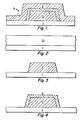
- a MIM diode 10 on a substrate 11 is shown. Overlying the substrate 11 is a first electrode 12 of about 200-500 nm thickness. The electrode 12 extends perpendicular to the plane of the drawing and contacts an address line of an LCD (not shown). Overlying the first electrode 12 is an insulator 14 having a thickness between about 35 and 80 nm. If this thickness is less than about 35 nm, pinholes can occur that short circuit the diode 10; for a thickness greater than about 80 nm, sufficiently non-linear MIM diode conduction does not occur.
- a second electrode 16 is opposed to the electrode 12, has a thickness between about 100 and 200 nm, overlies the insulator 14, and extends in the plane of the drawing to contact a pixel electrode (not shown).
- the substrate 11 can comprise an insulating material such as glass.
- the first electrode 12 can comprise a conductor such as a mixture of Ta and between about 10 and 50 atomic percent Si or between about 40 and 70 atomic percent Al.
- the insulator 14 comprises a mixture of Ta2O5 and another oxide typically having an average mole percent of between about 10 and 70.
- the other oxide can comprise between about 40 and 70 average mole percent Al2O3 or between about 10 and 50 average mole percent SiO2. These limits represent the ranges over which useful changes in resistivity occur as compared to a pure Ta2O5 insulator.
- average mole percent is meant the mole percent for the insulator 14 as a whole, even though at some locations, e.g., near the electrodes 12 and 14, the mole percent can differ.
- the second electrode 16 comprises a good conductor such as Al or Cr.
- a layer 12a is formed in a particular embodiment by radio frequency co-sputtering of Ta and Si or Ta and Al. A power density of about 2.3 watts/cm2 and an Ar pressure of about 15 millitorr, (about 2Pa) are used.
- the layer 12a is then defined into the first electrode 12 by reactive ion etching using, e.g., a plasma of CF4 and O2, as shown in FIGURE 3.
- the insulator 14 is formed by anodization using a 0.01% (by weight) citric acid solution, with the first electrode 12 being the anode (positive voltage applied thereto).
- the second electrode 16 is formed by vacuum deposition, such as evaporation or sputtering, to form the diode 10 of FIGURE 1. Thereafter, the diode 10 is annealed at about 250°C for about 20 minutes so that it has stable and repeatable characteristics.
- FIGURES 5 and 6 The general trend of the effective resistivity of the oxide mixtures is given in FIGURES 5 and 6 for Si and Al mixtures, respectively, wherein the voltage at a current density of 10 ⁇ A/mm2, V(10), is plotted as a function of the composition in atomic percent of the first electrode 12.
- V(1) is about 1 to 1.5 times the maximum possible stored voltage for a high contrast and high resolution display. All values for ⁇ , i o , and V(1) are averages for the two conduction directions since conduction in a MIM diode is asymmetrical.
- the first electrode comprised a mixture of Ta and about 29 atomic percent Si, which was anodized in dilute citric acid using a constant 30 volts for 3 hours to form the insulator 14 having a thickness of about 50 nm.
- the first electrode 12 comprised a mixture of Ta and about 36 atomic percent Si, which was anodized at a constant 24 volts for 3 hours to form the insulator 14 having a thickness of about 40 nm.
- ⁇ 4.8
- i o 2.4 ⁇ 10 ⁇ 10 A/mm2
- V(1) 3.0 volts.
- the first electrode 12 comprised a mixture of Ta and about 58 atomic percent Al, which was anodized at a constant 24 volts for 3 hours to form insulator 14 having a thickness of about 40 nm.
- ⁇ 4.1
- i o 2.8 ⁇ 10 ⁇ 10 A/mm2
- V(1) 4 volts.
- the first electrode 12 comprised nearly pure Ta that was anodized at a constant 30 volts for 3 hours to form insulator 14 having a thickness of about 50 nm.
- ⁇ 3.68
- i o 9.3 ⁇ 10 ⁇ 9 A/mm2
- V(1) 1.6 volts.
- diodes having a greater ⁇ and V(1) and a lower i o than the counter example, thereby resulting in a diode better suited to driving an LCD.
- the greater ⁇ provides better switching, and, further, sufficiently lower i o is obtained so that adequate charge storage is obtained at higher voltages.
- the dielectric constant of MIM diodes embodying the invention is lower compared to the prior art MIM diodes. This reduces parasitic shunt capacitance, thereby also contributing to a diode better suited to driving an LCD.
Landscapes
- Liquid Crystal (AREA)
- Glass Compositions (AREA)
- Control Of Motors That Do Not Use Commutators (AREA)
- Surface Acoustic Wave Elements And Circuit Networks Thereof (AREA)
Applications Claiming Priority (2)
| Application Number | Priority Date | Filing Date | Title |
|---|---|---|---|
| US93889086A | 1986-12-08 | 1986-12-08 | |
| US938890 | 1986-12-08 |
Publications (3)
| Publication Number | Publication Date |
|---|---|
| EP0271291A2 true EP0271291A2 (de) | 1988-06-15 |
| EP0271291A3 EP0271291A3 (en) | 1989-05-10 |
| EP0271291B1 EP0271291B1 (de) | 1993-05-26 |
Family
ID=25472146
Family Applications (1)
| Application Number | Title | Priority Date | Filing Date |
|---|---|---|---|
| EP87310658A Expired - Lifetime EP0271291B1 (de) | 1986-12-08 | 1987-12-03 | MIM-Diode mit gemischten Oxiden als Isolator |
Country Status (7)
| Country | Link |
|---|---|
| EP (1) | EP0271291B1 (de) |
| JP (1) | JPH0638526B2 (de) |
| KR (1) | KR930011475B1 (de) |
| CN (1) | CN1009602B (de) |
| DE (1) | DE3786001T2 (de) |
| FI (1) | FI91575C (de) |
| PT (1) | PT86306B (de) |
Cited By (7)
| Publication number | Priority date | Publication date | Assignee | Title |
|---|---|---|---|---|
| DE3929847A1 (de) * | 1989-09-08 | 1991-05-08 | Ernst Prof Dr Ing Lueder | Verfahren zur herstellung eines elektronischen schaltelementes |
| EP0395161A3 (de) * | 1989-04-28 | 1991-09-04 | Philips Electronics Uk Limited | MIM-Anordnung, Verfahren zu deren Herstellung und eine solche Anordnung enthaltende Anzeigevorrichtung |
| EP0629008A4 (de) * | 1992-12-28 | 1996-12-27 | Orion Electric Co Ltd | Struktur einer mim-diode und verfahren zu ihrer herstellung. |
| EP0636922A4 (de) * | 1993-02-10 | 1997-02-05 | Seiko Epson Corp | Nichtlineares wiederstandselement, verfahren zu seiner herstellung und fluessigkristall-anzeigevorrichtung. |
| DE19538128C1 (de) * | 1995-10-13 | 1997-02-27 | Lueder Ernst | Verfahren zur Herstellung eines elektronischen Schaltelementes |
| SG86965A1 (en) * | 1993-02-10 | 2002-03-19 | Seiko Epson Corp | Nonlinear resistance element, manufacturing fabrication method thereof, and liquid crystal display device |
| IT201900007572A1 (it) * | 2019-05-30 | 2020-11-30 | Green Arise Ltd | Diodo quantistico per trasformare una corrente alternata, in particolare una corrente alternata ad alta frequenza, in una corrente continua. |
Families Citing this family (2)
| Publication number | Priority date | Publication date | Assignee | Title |
|---|---|---|---|---|
| JP2006172159A (ja) * | 2004-12-16 | 2006-06-29 | Seiko Epson Corp | 電子デバイス製造システム、電子デバイスの製造方法、電子デバイス、並びに電気光学装置 |
| TWI422042B (zh) * | 2010-11-26 | 2014-01-01 | Univ Nat Chiao Tung | 二極體元件及其製作方法 |
Family Cites Families (7)
| Publication number | Priority date | Publication date | Assignee | Title |
|---|---|---|---|---|
| BE633414A (de) * | 1962-06-18 | 1900-01-01 | ||
| FR2505070B1 (fr) * | 1981-01-16 | 1986-04-04 | Suwa Seikosha Kk | Dispositif non lineaire pour un panneau d'affichage a cristaux liquides et procede de fabrication d'un tel panneau d'affichage |
| JPS5833221A (ja) * | 1981-08-21 | 1983-02-26 | Seiko Epson Corp | 液晶表示装置 |
| JPS58176622A (ja) * | 1982-04-09 | 1983-10-17 | Seiko Epson Corp | 電気光学装置 |
| DE3570782D1 (en) * | 1984-01-23 | 1989-07-06 | Energy Conversion Devices Inc | Liquid crystal displays operated by amorphous silicon alloy diodes |
| JPS60246686A (ja) * | 1984-05-22 | 1985-12-06 | Seiko Epson Corp | 薄膜非線形抵抗素子 |
| JPS62502069A (ja) * | 1985-02-25 | 1987-08-13 | アメリカン テレフオン アンド テレグラフ カムパニ− | 能動基板電気光学ディスプレイの温度補正 |
-
1987
- 1987-12-01 FI FI875296A patent/FI91575C/fi not_active IP Right Cessation
- 1987-12-03 EP EP87310658A patent/EP0271291B1/de not_active Expired - Lifetime
- 1987-12-03 DE DE87310658T patent/DE3786001T2/de not_active Expired - Fee Related
- 1987-12-04 PT PT86306A patent/PT86306B/pt not_active IP Right Cessation
- 1987-12-07 JP JP62310776A patent/JPH0638526B2/ja not_active Expired - Fee Related
- 1987-12-07 KR KR1019870013926A patent/KR930011475B1/ko not_active Expired - Fee Related
- 1987-12-08 CN CN87107422A patent/CN1009602B/zh not_active Expired
Cited By (8)
| Publication number | Priority date | Publication date | Assignee | Title |
|---|---|---|---|---|
| EP0395161A3 (de) * | 1989-04-28 | 1991-09-04 | Philips Electronics Uk Limited | MIM-Anordnung, Verfahren zu deren Herstellung und eine solche Anordnung enthaltende Anzeigevorrichtung |
| DE3929847A1 (de) * | 1989-09-08 | 1991-05-08 | Ernst Prof Dr Ing Lueder | Verfahren zur herstellung eines elektronischen schaltelementes |
| EP0629008A4 (de) * | 1992-12-28 | 1996-12-27 | Orion Electric Co Ltd | Struktur einer mim-diode und verfahren zu ihrer herstellung. |
| EP0636922A4 (de) * | 1993-02-10 | 1997-02-05 | Seiko Epson Corp | Nichtlineares wiederstandselement, verfahren zu seiner herstellung und fluessigkristall-anzeigevorrichtung. |
| SG86965A1 (en) * | 1993-02-10 | 2002-03-19 | Seiko Epson Corp | Nonlinear resistance element, manufacturing fabrication method thereof, and liquid crystal display device |
| DE19538128C1 (de) * | 1995-10-13 | 1997-02-27 | Lueder Ernst | Verfahren zur Herstellung eines elektronischen Schaltelementes |
| IT201900007572A1 (it) * | 2019-05-30 | 2020-11-30 | Green Arise Ltd | Diodo quantistico per trasformare una corrente alternata, in particolare una corrente alternata ad alta frequenza, in una corrente continua. |
| WO2020240603A1 (en) * | 2019-05-30 | 2020-12-03 | Green Arise Ltd | Quantum diode for transforming an alternating current, in particular high frequency alternating current, into a direct current |
Also Published As
| Publication number | Publication date |
|---|---|
| EP0271291A3 (en) | 1989-05-10 |
| FI91575B (fi) | 1994-03-31 |
| KR880008461A (ko) | 1988-08-31 |
| KR930011475B1 (ko) | 1993-12-08 |
| DE3786001D1 (de) | 1993-07-01 |
| FI91575C (fi) | 1994-07-11 |
| PT86306A (pt) | 1989-01-17 |
| JPH0638526B2 (ja) | 1994-05-18 |
| DE3786001T2 (de) | 1993-11-18 |
| FI875296L (fi) | 1988-06-09 |
| JPS63160286A (ja) | 1988-07-04 |
| CN1009602B (zh) | 1990-09-12 |
| CN87107422A (zh) | 1988-07-20 |
| EP0271291B1 (de) | 1993-05-26 |
| PT86306B (pt) | 1993-08-31 |
| FI875296A0 (fi) | 1987-12-01 |
Similar Documents
| Publication | Publication Date | Title |
|---|---|---|
| EP0466495B1 (de) | Flüssigkristall-Anzeigevorrichtung | |
| EP0430702B1 (de) | Werkstoff für elektrische Leiter, Elektronikagerät welches diesen verwendet und Flüssig-Kristall-Anzeige | |
| GB2091468A (en) | Matrix liquid crystal display device and method of manufacturing the same | |
| US4653858A (en) | Method of fabrication of diode-type control matrices for a flat electrooptical display screen and a flat screen constructed in accordance with said method | |
| EP0271291B1 (de) | MIM-Diode mit gemischten Oxiden als Isolator | |
| EP0395161B1 (de) | MIM-Anordnung, Verfahren zu deren Herstellung und eine solche Anordnung enthaltende Anzeigevorrichtung | |
| EP1171864A1 (de) | Elektronische anzeige | |
| US5274485A (en) | Liquid crystal display | |
| EP0440144A2 (de) | Substrat für Flüssigkristall-Anzeigevorrichtung | |
| US5053832A (en) | Nonlinear resistance element suitable for an active-type liquid crystal display | |
| US6710826B2 (en) | Two-terminal type non-linear element, manufacturing method and liquid crystal display panel | |
| EP0636922B1 (de) | Nichtlineares wiederstandselement, verfahren zu seiner herstellung und fluessigkristall-anzeigevorrichtung | |
| US5781256A (en) | Nonlinear resistance element and fabrication method thereof in which tungsten atoms are distributed continuously within the insulating film | |
| JPWO1994018600A1 (ja) | 非線形抵抗素子およびその製造方法ならびに液晶表示装置 | |
| US5478971A (en) | Metallic circuit board and thin film diode array and method of manufacturing the same | |
| JPH04269724A (ja) | 電気光学装置 | |
| EP0429296B1 (de) | Dielektrischer Heterofilm mit extrem niedrigem spezifischem Widerstand | |
| JPH0419557B2 (de) | ||
| JPH08262500A (ja) | 非線形素子を備えた固体装置 | |
| JPH02190826A (ja) | 液晶駆動用二端子素子 | |
| JPH07128689A (ja) | 表示装置 | |
| JPH04166817A (ja) | 液晶表示装置 | |
| JPH0695161A (ja) | 表示器用基板 | |
| JPH0583731U (ja) | 非線形素子を備えた固体装置 | |
| JPH06138494A (ja) | アクティブマトリクス型液晶表示装置およびその製造方法 |
Legal Events
| Date | Code | Title | Description |
|---|---|---|---|
| PUAI | Public reference made under article 153(3) epc to a published international application that has entered the european phase |
Free format text: ORIGINAL CODE: 0009012 |
|
| AK | Designated contracting states |
Kind code of ref document: A2 Designated state(s): DE ES FR GB IT |
|
| RAP1 | Party data changed (applicant data changed or rights of an application transferred) |
Owner name: GENERAL ELECTRIC COMPANY |
|
| PUAL | Search report despatched |
Free format text: ORIGINAL CODE: 0009013 |
|
| AK | Designated contracting states |
Kind code of ref document: A3 Designated state(s): DE ES FR GB IT |
|
| 17P | Request for examination filed |
Effective date: 19891023 |
|
| 17Q | First examination report despatched |
Effective date: 19920121 |
|
| GRAA | (expected) grant |
Free format text: ORIGINAL CODE: 0009210 |
|
| AK | Designated contracting states |
Kind code of ref document: B1 Designated state(s): DE ES FR GB IT |
|
| PG25 | Lapsed in a contracting state [announced via postgrant information from national office to epo] |
Ref country code: IT Free format text: LAPSE BECAUSE OF FAILURE TO SUBMIT A TRANSLATION OF THE DESCRIPTION OR TO PAY THE FEE WITHIN THE PRESCRIBED TIME-LIMIT;WARNING: LAPSES OF ITALIAN PATENTS WITH EFFECTIVE DATE BEFORE 2007 MAY HAVE OCCURRED AT ANY TIME BEFORE 2007. THE CORRECT EFFECTIVE DATE MAY BE DIFFERENT FROM THE ONE RECORDED. Effective date: 19930526 |
|
| REF | Corresponds to: |
Ref document number: 3786001 Country of ref document: DE Date of ref document: 19930701 |
|
| PG25 | Lapsed in a contracting state [announced via postgrant information from national office to epo] |
Ref country code: ES Free format text: LAPSE BECAUSE OF FAILURE TO SUBMIT A TRANSLATION OF THE DESCRIPTION OR TO PAY THE FEE WITHIN THE PRESCRIBED TIME-LIMIT Effective date: 19930906 |
|
| ET | Fr: translation filed | ||
| PLBE | No opposition filed within time limit |
Free format text: ORIGINAL CODE: 0009261 |
|
| STAA | Information on the status of an ep patent application or granted ep patent |
Free format text: STATUS: NO OPPOSITION FILED WITHIN TIME LIMIT |
|
| 26N | No opposition filed | ||
| PGFP | Annual fee paid to national office [announced via postgrant information from national office to epo] |
Ref country code: GB Payment date: 19941208 Year of fee payment: 8 |
|
| PG25 | Lapsed in a contracting state [announced via postgrant information from national office to epo] |
Ref country code: GB Effective date: 19951203 |
|
| GBPC | Gb: european patent ceased through non-payment of renewal fee |
Effective date: 19951203 |
|
| REG | Reference to a national code |
Ref country code: FR Ref legal event code: TP |
|
| REG | Reference to a national code |
Ref country code: FR Ref legal event code: D6 |
|
| PGFP | Annual fee paid to national office [announced via postgrant information from national office to epo] |
Ref country code: DE Payment date: 20041022 Year of fee payment: 18 |
|
| PGFP | Annual fee paid to national office [announced via postgrant information from national office to epo] |
Ref country code: FR Payment date: 20041209 Year of fee payment: 18 |
|
| PG25 | Lapsed in a contracting state [announced via postgrant information from national office to epo] |
Ref country code: DE Free format text: LAPSE BECAUSE OF NON-PAYMENT OF DUE FEES Effective date: 20060701 |
|
| PG25 | Lapsed in a contracting state [announced via postgrant information from national office to epo] |
Ref country code: FR Free format text: LAPSE BECAUSE OF NON-PAYMENT OF DUE FEES Effective date: 20060831 |
|
| REG | Reference to a national code |
Ref country code: FR Ref legal event code: ST Effective date: 20060831 |