EP0272390A2 - Empaquetages pour un dispositif semi-conducteur - Google Patents
Empaquetages pour un dispositif semi-conducteur Download PDFInfo
- Publication number
- EP0272390A2 EP0272390A2 EP87114577A EP87114577A EP0272390A2 EP 0272390 A2 EP0272390 A2 EP 0272390A2 EP 87114577 A EP87114577 A EP 87114577A EP 87114577 A EP87114577 A EP 87114577A EP 0272390 A2 EP0272390 A2 EP 0272390A2
- Authority
- EP
- European Patent Office
- Prior art keywords
- stem
- semiconductor chip
- semiconductor package
- wiring substrate
- holes
- Prior art date
- Legal status (The legal status is an assumption and is not a legal conclusion. Google has not performed a legal analysis and makes no representation as to the accuracy of the status listed.)
- Withdrawn
Links
Images
Classifications
-
- H—ELECTRICITY
- H10—SEMICONDUCTOR DEVICES; ELECTRIC SOLID-STATE DEVICES NOT OTHERWISE PROVIDED FOR
- H10W—GENERIC PACKAGES, INTERCONNECTIONS, CONNECTORS OR OTHER CONSTRUCTIONAL DETAILS OF DEVICES COVERED BY CLASS H10
- H10W70/00—Package substrates; Interposers; Redistribution layers [RDL]
- H10W70/60—Insulating or insulated package substrates; Interposers; Redistribution layers
- H10W70/62—Insulating or insulated package substrates; Interposers; Redistribution layers characterised by their interconnections
- H10W70/63—Vias, e.g. via plugs
- H10W70/635—Through-vias
-
- H—ELECTRICITY
- H10—SEMICONDUCTOR DEVICES; ELECTRIC SOLID-STATE DEVICES NOT OTHERWISE PROVIDED FOR
- H10W—GENERIC PACKAGES, INTERCONNECTIONS, CONNECTORS OR OTHER CONSTRUCTIONAL DETAILS OF DEVICES COVERED BY CLASS H10
- H10W70/00—Package substrates; Interposers; Redistribution layers [RDL]
- H10W70/60—Insulating or insulated package substrates; Interposers; Redistribution layers
- H10W70/67—Insulating or insulated package substrates; Interposers; Redistribution layers characterised by their insulating layers or insulating parts
- H10W70/68—Shapes or dispositions thereof
- H10W70/6875—Shapes or dispositions thereof being on a metallic substrate, e.g. insulated metal substrates [IMS]
-
- H—ELECTRICITY
- H10—SEMICONDUCTOR DEVICES; ELECTRIC SOLID-STATE DEVICES NOT OTHERWISE PROVIDED FOR
- H10W—GENERIC PACKAGES, INTERCONNECTIONS, CONNECTORS OR OTHER CONSTRUCTIONAL DETAILS OF DEVICES COVERED BY CLASS H10
- H10W76/00—Containers; Fillings or auxiliary members therefor; Seals
- H10W76/10—Containers or parts thereof
- H10W76/12—Containers or parts thereof characterised by their shape
- H10W76/15—Containers comprising an insulating or insulated base
- H10W76/153—Containers comprising an insulating or insulated base having interconnections in passages through the insulating or insulated base
-
- H—ELECTRICITY
- H10—SEMICONDUCTOR DEVICES; ELECTRIC SOLID-STATE DEVICES NOT OTHERWISE PROVIDED FOR
- H10W—GENERIC PACKAGES, INTERCONNECTIONS, CONNECTORS OR OTHER CONSTRUCTIONAL DETAILS OF DEVICES COVERED BY CLASS H10
- H10W90/00—Package configurations
- H10W90/701—Package configurations characterised by the relative positions of pads or connectors relative to package parts
- H10W90/731—Package configurations characterised by the relative positions of pads or connectors relative to package parts of die-attach connectors
- H10W90/737—Package configurations characterised by the relative positions of pads or connectors relative to package parts of die-attach connectors between a chip and a laterally-adjacent lead frame, conducting package substrate or heat sink
-
- H—ELECTRICITY
- H10—SEMICONDUCTOR DEVICES; ELECTRIC SOLID-STATE DEVICES NOT OTHERWISE PROVIDED FOR
- H10W—GENERIC PACKAGES, INTERCONNECTIONS, CONNECTORS OR OTHER CONSTRUCTIONAL DETAILS OF DEVICES COVERED BY CLASS H10
- H10W90/00—Package configurations
- H10W90/701—Package configurations characterised by the relative positions of pads or connectors relative to package parts
- H10W90/751—Package configurations characterised by the relative positions of pads or connectors relative to package parts of bond wires
- H10W90/754—Package configurations characterised by the relative positions of pads or connectors relative to package parts of bond wires between a chip and a stacked insulating package substrate, interposer or RDL
Definitions
- This invention relates to semiconductor packages, and more particularly to a type of semiconductor package suitable for use as a package for LSI having a number of output terminals.
- a typical example of a semiconductor package using pins for mounting the printed circuit board inserted therein is DIP (Dual In-line Package).
- DIP Device In-line Package
- the number of these output pins is limited, so that about 60 pins are the upper limit, more than 60 pins being practically unsuitable.
- PGA Peripheral Component Interconnect
- the PGA comprises the so-called ceramic type PGA using a laminate including a number of metal layers onto a ceramic substrate, or the so-called plastic type PGA using a plastic printed-circuit board instead of the wiring on said ceramic substrate in order to reduce the manufacturing cost thereof.
- said ceramic type PGA comprises the ceramic laminate type package
- the manufacturing process becomes generally complicated and costly.
- materials on the basis of tungsten are used for wiring, the resistance of this wiring becomes higher to cause a higher heating value, and the ceramic materials used have a relatively large heat capacity as well as a moderate heat radiation.
- plastic type PGA can be manufactured less costly than said ceramic type PGA, this type of PGA must be resin-sealed by means of organic materials for the purpose of protecting the semiconductor tips when these are mounted. Consequently, stress is occasionally applied from this sealing materials, and the characteristics of resins cause an incomplete isolation from the outer air so that a complete hermetic sealing cannot be obtained. Accordingly, the plastic type PGA is disadvantageous in that its fidelity is lower than that of said ceramic type PGA and that the size of tip which can be mounted therein is limited.
- the present invention helps to eliminate the above described disadvantages and the object thereof is to provide a semiconductor package which can be provided with a larger number of pins in order to be applied to the larger sizes of semiconductor tips while being completely hermetically sealed, and which can be manufactured at a lower cost.
- a semiconductor package which hermetically seals the corresponding semiconductor tip while the input and output terminals of the electric circuit formed on said semiconductor tip are held in the electrical connection with the outer circuits
- said semiconductor package comprising a metal stem having a semiconductor tip mounted at the center portion thereof and having a number of through-holes around the semiconductor tip; a wiring substrate attached on the upper surface of said stem, said substrate having a wiring layer of a predetermined pattern formed on the surface thereof and through-holes each corresponding to said through-holes of said stem; lead pins passing through said through-holes of said stem and said wiring substrate and protruding below said stem; and a shell for covering and hermetically sealing said semiconductor tip and said wiring substrate, wherein the input and output terminals of the electronic circuits formed on said semiconductor tip are connected with said wiring layer and this wiring layer is connected with said lead-pins.
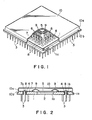
- the semiconductor package according to the present invention shown in the drawings comprises a plate-like stem 1 made of iron or ferroalloy such as 42 alloy, with a rectangular opening 1a formed at the substantially central portion thereof.
- a number of through-holes 1b, 1b,... are arranged around said opening 1a in three arrays from the circumference of said stem 1, said through-holes 1b each having the diameter of about 1 mm for passing therethrough the respective lead-pins 3.
- a circumferential portion 1c extends from a step portion.
- a heat sink member 2 (not shown in Fig. 1) of materials having a high heat radiation such as copper is seal-attached into said opening 1a of said stem 1.
- the improved heat radiation is thus obtained by using the heat sink member 2 and mounting the semiconductor chip 5 on the upper side of the heat sink 2 as will be described hereinbelow.
- the lead-pins 3 inserted into respective through-holes 1a of stem 1 are hermetically sealed therein at their respective upper portions by sealing materials 4 (not shown in Fig. 1) while protruding below the lower surface of the stem 1.
- Said semiconductor chip 5 is mounted and attached by soldering for example onto the upper surface of said heat sink 2.
- a wiring substrate 7 is fixed onto the upper surface of said stem 1.
- the size of this wiring substrate 7 is slightly smaller than that of said stem 1, so that, when the wiring substrate 7 is mounted on the upper surface of the stem 1, said circumferential portion 1c of stem 1 extends outside of the wiring substrate 7 for hermetically sealing thereon the circumference of the shell 10 as will be described hereinbelow.
- Wiring layer 6 (not shown in Fig. 2) having a predetermined wiring pattern is formed on said wiring substrate 7.
- the wiring substrate 7 comprises in general organic monolayer or laminate substrate of glass-epoxy resin, polyimide resin and the like, but ceramic substrates such as alumina or AlN can be used in combination with the materials of said stem 1.
- Through-holes 7a, 7a, ... for connection with one end of said wiring layer 6 are formed in the wiring substrate 7 respectively at the points corresponding to the through-holes 1b, 1b, ... bored in said stem 1.
- the upper portions of lead-pins 3 are inserted into respective through-holes 7a, with the upper end surface of each lead-pins 3 being connected with respective one end of the wiring layer 6 by means of junction materials 8 such as solder.
- Respective bonding pads as input-output terminals on said semiconductor chip 5 are connected with the other ends of the wiring layer 6 on said wiring substrate 7 through respective bonding wires 9 thereby to connect respective input-output terminals of semiconductor chip 5 with said respective lead-pins 3.
- a shell 10 such as metal cover having the vertical end wall 10a and the horizontal portion 10b extending therefrom is mounted on the upper surface of said wiring substrate 7.
- the inner side surface of said vertical end wall 10a abuts against the peripheral side surface of said wiring substrate 7, while said horizontally extending portion 10b of said shell 10 is superposed and hermetically sealed by electric welding, for example, onto the peripheral portion 1c of said stem 1.
- the semiconductor package according to the present invention renders possible the complete hermetic sealing which has been considered impossible with said plastic type PGA due to its proper characteristics.
- the hermetic sealing using glass between stem 1 and shell 10 can be carried out by equalizing the heat expansion coefficients of stem 1 and shell 10.
- semiconductor package according to the present invention it can be manufactured less costly than the ceramic type PGA and the plastic type PGA, and in addition thereto, its positive hermetic sealing assures a complete hermetic condition. Further, the adaptability to the larger type of packages substantially equivalent to that of ceramic PGA and the multi-pin construction substantially equivalent to that of plastic type PGA can be obtained according to the present invention though the latter characteristics are rather inferior to ceramic type PGA.
- the heat radiation is maximized and the electric capacity is minimized by utilizing polyimide resin or glass-epoxide resin as materials of wiring substrate.
Landscapes
- Lead Frames For Integrated Circuits (AREA)
- Cooling Or The Like Of Semiconductors Or Solid State Devices (AREA)
- Wire Bonding (AREA)
Applications Claiming Priority (2)
| Application Number | Priority Date | Filing Date | Title |
|---|---|---|---|
| JP61280225A JPH0773117B2 (ja) | 1986-11-25 | 1986-11-25 | 半導体パッケ−ジ |
| JP280225/86 | 1986-11-25 |
Publications (2)
| Publication Number | Publication Date |
|---|---|
| EP0272390A2 true EP0272390A2 (fr) | 1988-06-29 |
| EP0272390A3 EP0272390A3 (fr) | 1988-12-07 |
Family
ID=17622054
Family Applications (1)
| Application Number | Title | Priority Date | Filing Date |
|---|---|---|---|
| EP87114577A Withdrawn EP0272390A3 (fr) | 1986-11-25 | 1987-10-06 | Empaquetages pour un dispositif semi-conducteur |
Country Status (3)
| Country | Link |
|---|---|
| EP (1) | EP0272390A3 (fr) |
| JP (1) | JPH0773117B2 (fr) |
| KR (1) | KR900007301B1 (fr) |
Cited By (11)
| Publication number | Priority date | Publication date | Assignee | Title |
|---|---|---|---|---|
| DE3923533A1 (de) * | 1989-07-15 | 1991-01-24 | Diehl Gmbh & Co | Anordnung eines integrierten schaltkreises auf einem schaltungstraeger |
| EP0337448A3 (fr) * | 1988-04-13 | 1991-05-08 | Kabushiki Kaisha Toshiba | Dispositif semi-conducteur comprenant un support métallique |
| EP0360485A3 (fr) * | 1988-09-19 | 1991-07-17 | Advanced Micro Devices Inc. | Rangée de broches en forme de grille pour un paquet de circuits intégrés |
| WO1994022168A1 (fr) * | 1993-03-19 | 1994-09-29 | Olin Corporation | Boitier a systeme de reseau de billes pour dispositif electronique |
| EP0660399A3 (fr) * | 1993-12-20 | 1995-07-26 | Sgs Thomson Microelectronics | |
| EP0721212A1 (fr) * | 1989-11-29 | 1996-07-10 | Olin Corporation | Partie d'un boîtier électronique métallique |
| US5629835A (en) * | 1994-07-19 | 1997-05-13 | Olin Corporation | Metal ball grid array package with improved thermal conductivity |
| EP0862217A3 (fr) * | 1992-05-26 | 1999-12-15 | Motorola, Inc. | Dispositif semiconducteur et module semiconducteur à plusieure puces |
| EP1054445A1 (fr) * | 1999-05-19 | 2000-11-22 | Sagem Sa | Boítier électronique sur plaque et procédé de fabrication d'un tel boítier |
| EP1505860A1 (fr) * | 2003-08-08 | 2005-02-09 | Alps Electric Co., Ltd. | Module de circuit électronique pour montage en surface |
| DE10352705A1 (de) * | 2003-11-12 | 2005-06-23 | Diehl Bgt Defence Gmbh & Co. Kg | Schaltungsanordnung |
Families Citing this family (1)
| Publication number | Priority date | Publication date | Assignee | Title |
|---|---|---|---|---|
| JPH0243756A (ja) * | 1988-08-03 | 1990-02-14 | Toshiba Components Co Ltd | 半導体装置 |
Family Cites Families (4)
| Publication number | Priority date | Publication date | Assignee | Title |
|---|---|---|---|---|
| US3662230A (en) * | 1968-06-25 | 1972-05-09 | Texas Instruments Inc | A semiconductor interconnecting system using conductive patterns bonded to thin flexible insulating films |
| JPS5236824B2 (fr) * | 1973-10-15 | 1977-09-19 | ||
| JPS5113611A (en) * | 1974-07-19 | 1976-02-03 | Asahi Chemical Ind | Hiryobotono uchikomisochi |
| JPS6032770U (ja) * | 1983-08-12 | 1985-03-06 | 富士通株式会社 | 回路基板用リ−ドフレ−ム |
-
1986
- 1986-11-25 JP JP61280225A patent/JPH0773117B2/ja not_active Expired - Fee Related
-
1987
- 1987-10-06 EP EP87114577A patent/EP0272390A3/fr not_active Withdrawn
- 1987-11-25 KR KR1019870013294A patent/KR900007301B1/ko not_active Expired
Cited By (13)
| Publication number | Priority date | Publication date | Assignee | Title |
|---|---|---|---|---|
| EP0337448A3 (fr) * | 1988-04-13 | 1991-05-08 | Kabushiki Kaisha Toshiba | Dispositif semi-conducteur comprenant un support métallique |
| EP0360485A3 (fr) * | 1988-09-19 | 1991-07-17 | Advanced Micro Devices Inc. | Rangée de broches en forme de grille pour un paquet de circuits intégrés |
| DE3923533A1 (de) * | 1989-07-15 | 1991-01-24 | Diehl Gmbh & Co | Anordnung eines integrierten schaltkreises auf einem schaltungstraeger |
| EP0721212A1 (fr) * | 1989-11-29 | 1996-07-10 | Olin Corporation | Partie d'un boîtier électronique métallique |
| EP0862217A3 (fr) * | 1992-05-26 | 1999-12-15 | Motorola, Inc. | Dispositif semiconducteur et module semiconducteur à plusieure puces |
| WO1994022168A1 (fr) * | 1993-03-19 | 1994-09-29 | Olin Corporation | Boitier a systeme de reseau de billes pour dispositif electronique |
| EP0660399A3 (fr) * | 1993-12-20 | 1995-07-26 | Sgs Thomson Microelectronics | |
| US5629835A (en) * | 1994-07-19 | 1997-05-13 | Olin Corporation | Metal ball grid array package with improved thermal conductivity |
| EP1054445A1 (fr) * | 1999-05-19 | 2000-11-22 | Sagem Sa | Boítier électronique sur plaque et procédé de fabrication d'un tel boítier |
| FR2793990A1 (fr) * | 1999-05-19 | 2000-11-24 | Sagem | Boitier electronique sur plaque et procede de fabrication d'un tel boitier |
| US6212072B1 (en) | 1999-05-19 | 2001-04-03 | Sagem Sa | Electronics package on a plate, and a method of making such a package |
| EP1505860A1 (fr) * | 2003-08-08 | 2005-02-09 | Alps Electric Co., Ltd. | Module de circuit électronique pour montage en surface |
| DE10352705A1 (de) * | 2003-11-12 | 2005-06-23 | Diehl Bgt Defence Gmbh & Co. Kg | Schaltungsanordnung |
Also Published As
| Publication number | Publication date |
|---|---|
| KR880006773A (ko) | 1988-07-25 |
| EP0272390A3 (fr) | 1988-12-07 |
| JPH0773117B2 (ja) | 1995-08-02 |
| KR900007301B1 (ko) | 1990-10-08 |
| JPS63133553A (ja) | 1988-06-06 |
Similar Documents
| Publication | Publication Date | Title |
|---|---|---|
| US5789811A (en) | Surface mount peripheral leaded and ball grid array package | |
| US3760090A (en) | Electronic circuit package and method for making same | |
| US5677575A (en) | Semiconductor package having semiconductor chip mounted on board in face-down relation | |
| US5247423A (en) | Stacking three dimensional leadless multi-chip module and method for making the same | |
| US5404273A (en) | Semiconductor-device package and semiconductor device | |
| US5886876A (en) | Surface-mounted semiconductor package and its manufacturing method | |
| US5307240A (en) | Chiplid, multichip semiconductor package design concept | |
| US6002168A (en) | Microelectronic component with rigid interposer | |
| US5976914A (en) | Method of making plastic package for a surface mounted integrated circuit | |
| US20070273049A1 (en) | Interconnect structure and formation for package stacking of molded plastic area array package | |
| EP0670594B1 (fr) | Empaquetage pour semi-conducteur | |
| US4054938A (en) | Combined semiconductor device and printed circuit board assembly | |
| GB2188485A (en) | Integrated circuit chip mounting and packaging assembly | |
| US6054767A (en) | Programmable substrate for array-type packages | |
| EP0272390A2 (fr) | Empaquetages pour un dispositif semi-conducteur | |
| JP2573809B2 (ja) | 電子部品内蔵のマルチチップモジュール | |
| KR100226335B1 (ko) | 플라스틱 성형회로 패키지 | |
| US6166435A (en) | Flip-chip ball grid array package with a heat slug | |
| US6320136B1 (en) | Layered printed-circuit-board and module using the same | |
| US5872026A (en) | Process of fabricating an integrated circuit die package having a plurality of pins | |
| JP3656861B2 (ja) | 半導体集積回路装置及び半導体集積回路装置の製造方法 | |
| JP3210503B2 (ja) | マルチチップモジュールおよびその製造方法 | |
| JPS63229842A (ja) | 表面実装用パツケ−ジ | |
| KR100251860B1 (ko) | Csp (칩 스케일 패키지)의 구조 및 제조방법 | |
| JP2786047B2 (ja) | 樹脂封止型半導体装置 |
Legal Events
| Date | Code | Title | Description |
|---|---|---|---|
| PUAI | Public reference made under article 153(3) epc to a published international application that has entered the european phase |
Free format text: ORIGINAL CODE: 0009012 |
|
| 17P | Request for examination filed |
Effective date: 19871006 |
|
| AK | Designated contracting states |
Kind code of ref document: A2 Designated state(s): DE FR GB |
|
| PUAL | Search report despatched |
Free format text: ORIGINAL CODE: 0009013 |
|
| AK | Designated contracting states |
Kind code of ref document: A3 Designated state(s): DE FR GB |
|
| 17Q | First examination report despatched |
Effective date: 19920213 |
|
| STAA | Information on the status of an ep patent application or granted ep patent |
Free format text: STATUS: THE APPLICATION IS DEEMED TO BE WITHDRAWN |
|
| 18D | Application deemed to be withdrawn |
Effective date: 19920825 |
|
| RIN1 | Information on inventor provided before grant (corrected) |
Inventor name: SHINDO, MASAMICHI |