EP0276340B1 - Ecran matriciel comportant des transistors composés - Google Patents
Ecran matriciel comportant des transistors composés Download PDFInfo
- Publication number
- EP0276340B1 EP0276340B1 EP87101033A EP87101033A EP0276340B1 EP 0276340 B1 EP0276340 B1 EP 0276340B1 EP 87101033 A EP87101033 A EP 87101033A EP 87101033 A EP87101033 A EP 87101033A EP 0276340 B1 EP0276340 B1 EP 0276340B1
- Authority
- EP
- European Patent Office
- Prior art keywords
- electrode
- source
- display
- gate
- pattern
- Prior art date
- Legal status (The legal status is an assumption and is not a legal conclusion. Google has not performed a legal analysis and makes no representation as to the accuracy of the status listed.)
- Expired
Links
- 239000011159 matrix material Substances 0.000 title claims abstract description 8
- 239000002131 composite material Substances 0.000 title claims abstract description 7
- 239000004065 semiconductor Substances 0.000 claims abstract description 14
- 239000010409 thin film Substances 0.000 abstract description 44
- 239000004973 liquid crystal related substance Substances 0.000 abstract description 19
- 238000010586 diagram Methods 0.000 description 15
- 239000010408 film Substances 0.000 description 13
- 239000000758 substrate Substances 0.000 description 10
- 238000004519 manufacturing process Methods 0.000 description 6
- 230000003071 parasitic effect Effects 0.000 description 4
- 230000007423 decrease Effects 0.000 description 3
- 230000004048 modification Effects 0.000 description 3
- 238000012986 modification Methods 0.000 description 3
- 229910021417 amorphous silicon Inorganic materials 0.000 description 2
- 239000006185 dispersion Substances 0.000 description 2
- 125000006850 spacer group Chemical group 0.000 description 2
- 229910052581 Si3N4 Inorganic materials 0.000 description 1
- XAGFODPZIPBFFR-UHFFFAOYSA-N aluminium Chemical compound [Al] XAGFODPZIPBFFR-UHFFFAOYSA-N 0.000 description 1
- 229910052782 aluminium Inorganic materials 0.000 description 1
- 238000003491 array Methods 0.000 description 1
- 210000002858 crystal cell Anatomy 0.000 description 1
- 239000011521 glass Substances 0.000 description 1
- -1 i.e. Substances 0.000 description 1
- HQVNEWCFYHHQES-UHFFFAOYSA-N silicon nitride Chemical compound N12[Si]34N5[Si]62N3[Si]51N64 HQVNEWCFYHHQES-UHFFFAOYSA-N 0.000 description 1
Images




Classifications
-
- G—PHYSICS
- G02—OPTICS
- G02F—OPTICAL DEVICES OR ARRANGEMENTS FOR THE CONTROL OF LIGHT BY MODIFICATION OF THE OPTICAL PROPERTIES OF THE MEDIA OF THE ELEMENTS INVOLVED THEREIN; NON-LINEAR OPTICS; FREQUENCY-CHANGING OF LIGHT; OPTICAL LOGIC ELEMENTS; OPTICAL ANALOGUE/DIGITAL CONVERTERS
- G02F1/00—Devices or arrangements for the control of the intensity, colour, phase, polarisation or direction of light arriving from an independent light source, e.g. switching, gating or modulating; Non-linear optics
- G02F1/01—Devices or arrangements for the control of the intensity, colour, phase, polarisation or direction of light arriving from an independent light source, e.g. switching, gating or modulating; Non-linear optics for the control of the intensity, phase, polarisation or colour
- G02F1/13—Devices or arrangements for the control of the intensity, colour, phase, polarisation or direction of light arriving from an independent light source, e.g. switching, gating or modulating; Non-linear optics for the control of the intensity, phase, polarisation or colour based on liquid crystals, e.g. single liquid crystal display cells
- G02F1/133—Constructional arrangements; Operation of liquid crystal cells; Circuit arrangements
- G02F1/136—Liquid crystal cells structurally associated with a semi-conducting layer or substrate, e.g. cells forming part of an integrated circuit
- G02F1/1362—Active matrix addressed cells
- G02F1/1368—Active matrix addressed cells in which the switching element is a three-electrode device
Definitions
- This invention relates to thin film transistors which are employed for driving pixels (i.e., picture elements) of an active matrix type flat panel display such as a liquid crystal display device, for example.
- a prior art liquid crystal display device of the conventional type has a structure as shown in Fig. 1.
- the device comprises a pair of transparent substrates of glass or the like facing each other.
- a spacer 13 is provided between the substrates 11 and 12 along the edges thereof.
- a liquid crystal 14 is sealed between the substrates 11 and 12.
- the substrates 11 and 12, spacer 13 and liquid crystal 14 constitute a liquid crystal cell.
- a plurality of display electrodes 15 consisting of a transparent conductive film are formed on the inner surface of one of the transparent substrates, i.e., substrate 11.
- thin film transistors 16 are formed as switching elements such that they are contiguous to the display electrodes 15 with their drains connected thereto.
- a common electrode 17 is formed on the other transparent substrate 12. The common electrode 17 faces the plurality of display electrodes 15.
- the display electrodes 15 serve as to provide picture elements, for instance. As shown in Fig. 2, they are square in shape and arranged in a closely spaced apart relation to one another. They are arranged in rows and columns on the transparent substrate 11. Gate buses 18 are formed such that they extend near and along the individual rows of display electrodes 15. Source buses 19 are formed such that they extend near and along the individual columns of display electrodes 15. The thin film transistors 16 noted above are formed at the intersections of the gate buses 18 and source buses 19. Each thin film transistor 16 has its gate connected to the associated gate bus 18, its source connected to the associated source bus 19 and its drain connected to the corresponding display electrode 15.
- the thin film transistor 16 has a structure as shown in Figs. 3 and 4.
- the display electrodes 15 and source buses 19 are formed from a transparent conductive film, e.g., an ITO, on the transparent substrate 11.
- a semiconductor layer 21 of amorphous silicon or the like is formed such that it strides parallel and closely spaced-apart portions of each display electrode 15 and the associated source bus 19.
- a gate insulating film 22 of silicon nitride or the like is formed on the semiconductor layer 21.
- a gate electrode 23 is formed on the gate insulating film 22 such that it overlies part of each display electrode 15 and associated source bus 19 via the gate insulating film 22 and each semiconductor layer 21. One end of the gate electrode 23 is connected to the associated gate bus 18.
- Portions of the display electrode 15 and source bus 19 facing each gate electrode 23 constitute drain and source electrodes 15a and 19a, respectively.
- the thin film transistor 16 is constituted by these electrodes 15a and 19a, the semiconductor layer 21, the gate insulating film 22 and the gate electrode 23.
- the individual gate electrodes 23 and gate buses 18 are formed simultaneously from aluminum, for instance.
- electrostatic (parasitic) capacitances Cgd and Csg are formed between the gate electrode 23 of each thin film transistor 16 and its drain and source electrodes 15a and 19a, respectively. Further, a parasitic resistance Rs exists whose value depends upon the area of the semiconductor layer 21 between the gate electrode 23 and each of the drain and source electrodes 15a and 19a. The electrostatic capacitances Cgd and Csg and the parasitic resistance Rs exert a great influence on the characteristics of the thin film transistor 16.
- Fig. 5 schematically illustrates an example of the liquid crystal display device employing such a structure.
- the display electrodes 15 are arranged in a matrix form, and as in the cases of Figs. 2 and 3, the source bus 19 is formed along one side of each column of the display electrodes 15 and connected to each display electrode 15 via the thin film transistor 16.
- a thin film transistor 25 is connected to each display electrode 15 at the side opposite from the thin film transistor 16, that is, at the left of the display electrode 15 in Fig. 5.
- Extending along each column of the display electrodes 15 at the opposite side from the source bus 19 is another source bus 26, to which are connected source electrodes of the thin film transistors 25.
- the pair of source buses 19 and 26 for each column of the display electrodes 15 are interconnected at both ends, forming a loop.
- the thin film transistor 25 has its gate electrode connected to the gate bus 18 to which is connected the gate electrode of the thin film transistor 16 connected to the display electrode 15 corresponding thereto. Accordingly, the both thin film transistors 16 and 25 are connected in parallel to each other for each display electrode 15.
- the source bus 26 are formed along one side of each column of display electrodes 15 opposite side from the source bus 19.
- An amorphous silicon or like semiconductor layer 27 is extended between the source bus 26 and each display electrode 15 and is covered with the gate insulating film 22, on which a gate electrode 28 is formed, thus constituting each thin film transistor 25.
- the gate electrode 28 is connected to the gate bus 18.
- the pair thin film transistors 16 and 25 are disposed on both sides of each display electrode 15 and are connected in parallel to each other; so that, letting the electrostatic capacitances set up between the gate electrode 23 and the display electrode 15 and the source bus 19 be represented by Cgd1 and Csg1, respectively, the electrostatic capacitances Cgd1 and Cgd2 and the electrostatic capacitances Csg1 and Csg2 are connected in parallel to each other.
- the electrostatic capacitances Cgd1 + Cgd2 and Csg1 + Csg2 are each 3w, namely, that each gate electrode overlaps the drain and source electrodes 3 ⁇ m and the channel width is w/2.
- the gate electrodes 23 and 28 of the thin film transistor 25 are formed simultaneously using the same mask; so that, for instance, when the gate electrode 23 shifts to the right-hand side in Figs. 6, 7 and 8, the gate electrode 28 also shifts to the right-hand side by the same amount.
- the electrostatic capacitances can always be obtained at designed values. Accordingly, even where misalignment of the mask for forming the gate electrodes is not uniform throughout the display screen of the liquid crystal display device, thin film transistors of the same characteristics can be obtained.
- the sum of the parasitic resistances Rs is also constant at all times because the resistance on the side of the thin film transistor 25 decreases when the resistance on the side of the thin film transistor 16 increases.
- the bus for supplying a source or gate signal is approximately twice as long as in ordinary liquid crystal display devices, and the spacing of the source or gate buses is so small that they are often broken and short-circuited during manufacture, impairing the yield rate of fabrication of the display devices.
- EP-A-209 113 also describes an arrangement similar to that in US-A-4 59 70 01.
- a display device having a plurality of display electrodes, each one connectd to a source bus and to a gate, bus by means of a pixel driving composite transistor,each transistor comprising: an even number of source electrode portions connected to a source bus, an even number of drain electrode portions respectively disposed adjacent the source electrode portions and connected to the same display electrode,the drain electrode portions being arranged with respect to the source electrode portions such that the direction from half said number of drain electrode portions to their corresponding source electrode portions is opposite to the direction from the other half of said number of drain electrode portions to their corresponding source electrode portions, a semiconductor layer provided in common to all the source and drain electrode portions a gate insulating film formed on the semiconductor layer and a gate electrode having two opposite side edge portions disposed on the gate insulating film common to all the source and drain electrode portions such that one of the side edge portions of the gate electrode covers either half said number of source electrode portions or half said number of drain electrode portions and the opposite side edge portion of the gate electrode covers the other half of said number of source electrode portions or the
- the plurality of pairs of source and drain electrodes are provided such that the number of pairs of the source and drain electrodes arranged in the same order in one direction is equal to the number of pairs of the source and drain electrodes arranged in the same order in opposite direction and both electrodes are disposed opposite a gate insulating film and a gate electrode common to them.
- the gate electrode is common to the plurality of source and drain electrodes, the source and gate buses need not be extended long and the number of source or gate buses need not be increased either, ensuring the reduction of accidents such as short-circuiting of adjoining buses and breakage of buses.
- Fig. 1 is a cross-sectional view showing a part of the general structure of prior art liquid crystal display device
- Fig. 2 is a schematic circuit diagram of an active matrix liquid crystal display device
- Fig. 3 is a plan view showing the arrangement of display electrodes 15 and transistors 16 of the liquid crystal display device depicted in Fig. 1;
- Fig. 4 is a cross-sectional view taken on the line 4-4 in Fig. 3;
- Fig. 5 is a diagram schematically showing the relationship between display electrodes 15, transistors 16, 25 and source buses 19, 26 of an improved liquid crystal display device
- Fig. 6 is a plan view, similar to Fig. 3, of the liquid crystal display device shown in Fig. 5;
- Fig. 7 is a cross-sectional view taken on the line 7-7 in Fig. 6;
- Fig. 8 is a diagram showing overlaps of a gate electrode on source and drain electrodes in Fig. 6;
- Fig. 9 is a plan view showing arrays of transistors and display electrodes in the case where an example of array of the pixel driving transistors of the present invention is applied to an active matrix liquid crystal display device;
- Fig. 10 is a plan view, similar to Fig. 9, showing an example in which the transistors of the present invention are disposed between branched patterns of the source bus and the display electrode;
- Fig. 11 is a diagram, similar to Fig. 9, illustrating an example in which four source electrodes and four drain electrodes are defined at opposite edge portions of the branched patterns of the source bus and the display electrode under the gate bus;
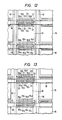
- Fig. 12 is a diagram illustrating a modified form of the present invention in which the gate bus is shifted widthwise thereof in Fig. 11;
- Fig. 13 is a diagram, similar to Fig. 9, illustrating another example of the present invention in which four source electrodes and four drain electrodes are defined at opposite edge portions of the branched patterns of the source bus and the display electrode under the gate bus;
- Fig. 14 is a diagram illustrating another modification in which the gate bus is shifted widthwise thereof in Fig. 13;
- Fig. 15 is a diagram, similar to Fig. 9, illustrating another example of the present invention in which numbers of source and drain electrodes are defined at opposite edge portions of the branched patterns of the source bus and the display electrode under the gate bus;
- Fig. 16 is a diagram, similar to Fig. 9, illustrating the case where source and drain electrodes are defined at opposite edge portions of the branched patterns of the source bus and the display electrode under a branched pattern of the gate bus;
- Fig. 17 is a diagram, similar to Fig. 11, illustrating an example in which four source electrodes and four drain electrodes are defined under a branched pattern of the gate bus;
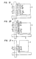
- Fig. 18 is a diagram illustrating a modified form of the structure of Fig. 17 in which the gate electrode 23 is shifted;
- Fig. 19 is a diagram, similar to Fig. 13, showing an example in which four drain electrodes and four source electrodes are defined under a branched pattern of the gate bus;
- Fig. 20 is a diagram illustrating a modified form of the structure of Fig. 19 in which the gate electrode 23 is shifted;
- Fig. 21 is a diagram illustrating an example in which two source electrodes and two drain electrodes are aligned between the source bus and the display electrode.
- Fig. 9 is a schematic diagram, similar to Figs. 3 and 6, illustrating the pixel driving thin film transistors of the present invention which are applied to an active matrix liquid crystal display device, the parts corresponding to those in Figs. 3 and 6 being identified by the same reference numerals.
- the source bus 19 branches out at right angles, extending along one marginal portion of each display electrode 15, as indicated by 31, and one half of this marginal portion is staggered relative to the other half thereof, as shown.
- the branched pattern 31 is staggered to extend along the recessed marginal portion, and the staggered portion 32 is surrounded by a branched pattern 33 extending from the display electrode 15.
- An amorphous semiconductor layer 21 is formed to extend over the opposing marginal portions of the display electrode 15 and the branched pattern 31 and the opposing marginal portions of the staggered portion 32 and the branched pattern 33. Then, the gate insulating film 22 (not shown) is extended over the entire surface of the substrate. The gate bus 18 is formed on the gate insulating film 22 so that it overlaps the display electrode 15, the branched pattern 31, its staggered portion 32, and the branched pattern 33.
- the portions of the display electrode 15 and the branched pattern 33 which are opposed to the gate bus 18 serve as the drain electrodes 15a and 15b, respectively, and the portions of the branched pattern 31 and the staggered portion 32 which are opposed to the gate bus 18 serve as the source electrodes 19a and 19b, respectively.
- the drain and source electrodes 15a and 19a and those 15b and 19b are arranged in parallel but opposite in direction, and these electrodes 15a, 15b, 19a and 19b are opposite the common gate electrode (i.e., the gate bus 18) via the common semiconductor layer 21 and the gate insulating film 22.
- the channels between the electrodes 15a and 19a and between the electrodes 15b and 19b are equal in length and in width and are aligned in a width direction.
- the drain electrode 15a, the source electrode 19a, and the gate bus 18 constitute parts of the thin film transistor 16
- the drain electrode 15b, the source electrode 19b, and the gate bus 18 constitute parts of a thin film transistor 34.
- the thin film transistors 16 and 34 are connected in parallel to each other and operate as one composite transistor. It will easily be understood that even if the gate bus 18 is formed out of position in the direction of arrangement of the drain and source electrodes 15a and 19a owing to misalignment of the mask during fabrication, the gate-source capacitance and gate-drain capacitance of the transistor composed of the parallel-connected thin film transistors 16 and 34 will remain constant.
- the gate bus 18 and the source bus 19 have substantially the same lengths as in the case of Fig. 3, and need not be lengthened.
- two source buses are disposed between adjoining columns of display electrodes, whereas in this example only one source bus is provided; accordingly, the possibility of breakage of the source bus 19 diminishes and no short-circuiting occurs.
- branched pattern 32 of the source bus 19 is extended along substantially the entire length of one marginal edge of the display electrode 15 and is surrounded by the branched pattern of the display electrode 15.
- the gate bus 18 is provided so that it is partly opposed to the branched pattern 32, the display electrode 15, and the branched pattern 32.
- one marginal portion of the branched pattern 32 of the gate bus 18 acts as the source electrode 19a and the opposite marginal portion as the source electrode 19b.
- the number of source-drain electrode pairs is not limited specifically to two, but can be greater provided that there are an equal number of pairs in both opposite source-drain arrangement directions.
- Fig. 11 illustrates an example in which two such electrode pairs are provided in each of opposite directions.
- a pair of the drain electrode 15a and the source electrode 19a and a pair of the source electrode 19b and the drain electrode 15b are arranged widthwise of the gate bus 18 in opposite directions. Adjacent these electrodes in lengthwise direction of the gate bus 18, a pair of drain electrode 15c and source electrode 19c and a pair of source electrode 19d and drain electrode 15d are similarly arranged widthwise of the gate bus 18 in opposite direction.
- the drain electrodes 15a and 15c are defined along one marginal portion of the display electrode 15, to the both ends of which are connected the drain electrodes 15b and 15d.
- the source electrodes 19a to 19d are defined along the pattern 32 which extends along one marginal edge of the display electrode 15, and the pattern 32 is connected at its intermediate portion to the branched pattern 31.
- Fig. 12 illustrates a modified form of the example shown in Fig. 11, in which the gate bus 18 is shifted widthwise thereof so that it overlaps the branched pattern 31 but does not overlap the display electrode 15.
- Fig. 13 illustrates another modification of the structure of Fig. 11, in which the drain electrodes 15b and 15d are both connected to the display electrode 15 at the intermediate portion of one marginal edge thereof, the source electrodes 19a and 19b are formed as one electrode 32, and the source electrodes 19c and 19d are also formed as one electrode 32 connected at one end to the branched pattern 31. That is, the branched pattern 33 is formed along one marginal edge of the display electrode 15, and the intermediate portion of the branched pattern 33 is connected to the display electrode 15.
- Fig. 14 shows a modified form of the structure depicted in Fig. 13, in which the gate bus 18 is shifted widthwise thereof, as is the case with Fig. 12.
- Fig. 15 illustrates another example in which more electrode pairs are provided.
- the branch pattern 31 of the source bus 19 is formed, a plurality of transistors are provided between the branch pattern 31 and the display electrode 15, and the gate bus itself is used as the gate electrode common to the transistors.
- the present invention is also applicable to such a structure as depicted in Fig. 3 in which a transistor is formed between the source bus 19 and the display electrode 15 and its gate electrode is formed by a branch of the gate bus. Examples of this structure are shown in Figs. 16 through 21, in which the parts corresponding to those in the above are identified by the same reference numerals. In Fig. 16 which corresponds to Fig.
- Fig. 17 illustrates another example which is identical in structure with the example of Fig. 11.
- Figs. 18, 19 and 20 show other examples which correspond to those of Figs. 12, 13 and 14.
- One half portion of the extended pattern 33 in Fig. 20 may also be omitted, as shown in Fig. 21.
Landscapes
- Physics & Mathematics (AREA)
- Nonlinear Science (AREA)
- Engineering & Computer Science (AREA)
- Microelectronics & Electronic Packaging (AREA)
- Mathematical Physics (AREA)
- Chemical & Material Sciences (AREA)
- Crystallography & Structural Chemistry (AREA)
- General Physics & Mathematics (AREA)
- Optics & Photonics (AREA)
- Liquid Crystal (AREA)
- Thin Film Transistor (AREA)
- Control Of El Displays (AREA)
Claims (8)
- Dispositif d'affichage comportant une multiplicité d'électrodes d'affichage, dont chacune est reliée à un bus de source et à un bus de grille au moyen d'un transistor composite de commande de pixels, chaque transistor comprenant:
un nombre pair de parties d'électrodes de source (19a,19b,19c,19d) reliées à un bus de source (19);
Un nombre pair de parties d'électrodes de drain (15a,15b,15c,15d) disposées respectivement au voisinage de parties d'électrodes de source (19a,19b,19c,19d) et reliées à la m électrode d'afflchage (15), les parties d'électrodes de drain (15a,l5b,15c,15d) étant disposées par rapport aux parties d'électrodes de source (19a,19b,19c,19d) de telle manière que la direction depuis la moitié dudit nombre de parties d'électrodes de drain (l5a,l5b,15c,l5d) vers leurs parties d'électrodes de source correspondantes (19a,19b,l9c,19d) soit opposée à la direction depuis l'autre moitié dudit nombre de parties d'électrodes de drain (15a,l5b,15c,15d) vers leurs parties d'électrodes de source correspondantes (19a,19b,19c,19d);
une couche de semiconducteur (21) prévue de façon à être commune à toutes les parties d'électrodes de source et de drain (15a,15b,15c,15d); (19a,19b,19c,19d);
un film d'isolement de grille (22) formé sur la couche de semiconducteur (21); et
une électrode de grille (23) ayant deux parties de bords latéraux opposées disposées sur le film d'isolement de grille (22) en commun avec toutes les parties d'électrdes de source et de drain (15a,15b,15c,15d;19a,19b,19c,19d), caractérisé en ce que l'une des parties de bord latéral de l'électrode de grille (23) couvre soit la moitié dudit nombre de parties d'électrodes de source soit la moitié dudit nombre de parties d'électrode de drain (15a,15c;19a,19c) et la partie de bord latéral opposée de l'électrode de grille (23) couvre l'autre moitié dudit nombre de parties d'électrode de source ou l'autre moitié dudit nombre de parties d'électrodes de drain-(15b,15d;19b,19d). - Dispositif d'affichage selon la revendication 1, dans lequel les électrodes d'affichage sont des électrodes carrées disposées sous la forme d'une matrice, un bus de grille est prévu pour chaque rangée d'électrodes d'affichage, le bus de source est l'un de ceux prévus pour les colonnes respectives d'électrodes d'affichage, et les bus de grille et de source et chaque électrode d'affichage sont reliés via le transistor composite au voisinage de chaque intersection des bus.
- Dispositif d'affichage selon la revendication 2, dans lequel le bus de source ou une configuration dérivée de celui-ci comporte une extension s'étendant parallèlement au bus de source ou à sa configuration de branchement, l'électrode d'affichage comporte une configuration étendue s'étendant entre l'extension du bus de source et le bus de source ou sa configuration de branchement qui lui est parallèle, et l'électrode de grille est prévue de façon à couvrir le bus de source ou la configuration de branchement et son extension.
- Dispositif d'affichage selon la revendication 2, dans lequel le bus de source ou une configuration dérivée de celui-ci comporte une extension s'étendant parallèlement au bus de source ou à sa configuration de branchement, l'électrode d'affichage comporte une configuration étendue s'étendant entre l'extension du bus de source et le bus de source ou sa configuration de branchement qui lui est parallèle, et l'électrode de grille est prévue de façon à couvrir la configuration étendue de l'électrode d'affichage et l'électrode d'affichage.
- Dispositif d'affichage selon la revendication 3 ou la revendication 4, dans lequel le bus de source comporte une seconde extension, allant du point de connexion de la première extension vers le bus de source ou la configuration de branchement dans la direction opposée à la première extension, l'électrode d'affichage comporte une seconde configuration étendue s'étendant entre la seconde extension du bus de source et le bus de source ou la configuration de branchement, et l'électrode de grille est étendue suivant la même largeur sur la seconde extension et la seconde configuration étendue.
- Dispositif d'affichage selon la revendication 3 ou la revendication 4, dans lequel l'électrode d'affichage comporte une seconde configuration étendue, à partir du point de connexion de la première extension vers l'électrode d'affichage dans la direction opposée à celle de la première extension, le bus de source ou sa configuration de branchement comporte une seconde extension s'étendant entre la seconde configuration étendue et l'électrode d'affichage, et l'électrode de grille est étendue suivant la même largeur sur la seconde configuration étendue et la seconde extension.
- Dispositif d'affichage selon la revendication 2, dans lequel le bus de source comporte une configuration de branchement s'étendant sensiblement perpendiculairement à sa direction le long d'un bord marginal de l'électrode d'affichage, la configuration de branchement comporte une extension disposée plus près de l'électrode d'affichage que l'extrémité d'extension de la configuration de branchement et positionnée dans un évidement réalisé dans le bord marginal de l'électrode d'affichage, l'électrode d'affichage comporte une configuration étendue s'étendant le long de l'extension du bus de source de son côté opposé à l'électrode d'affichage, et un bus de grille s'étendant entre la configuration de branchement et l'électrode d'affichage et entre la configuration étendue et l'extension du bus de source joue le rôle d'électrode de grille.
- Dispositif d'affichage selon la revendication 2, dans lequel le bus de source comporte une configuration de branchement s'étendant sensiblement perpendiculairement à sa direction le long d'un bord marginal de l'électrode d'affichage, l'électrode d'affichage comporte une configuration étendue s'étendant le long de la configuration de branchement de son côté opposé à l'électrode d'affichage, et un bus de grille formé de façon à recouvrir la configuration étendue, la configuration de branchement et l'électrode d'affichage, joue le rôle d'électrode de grille.
Priority Applications (4)
| Application Number | Priority Date | Filing Date | Title |
|---|---|---|---|
| US07/004,405 US4762398A (en) | 1987-01-26 | 1987-01-20 | Pixel transistor free of parasitic capacitance fluctuations from misalignment |
| EP87101033A EP0276340B1 (fr) | 1987-01-26 | 1987-01-26 | Ecran matriciel comportant des transistors composés |
| DE8787101033T DE3768643D1 (de) | 1987-01-26 | 1987-01-26 | Matrixanzeige mit zusammengesetzten transistoren. |
| AT87101033T ATE61673T1 (de) | 1987-01-26 | 1987-01-26 | Matrixanzeige mit zusammengesetzten transistoren. |
Applications Claiming Priority (1)
| Application Number | Priority Date | Filing Date | Title |
|---|---|---|---|
| EP87101033A EP0276340B1 (fr) | 1987-01-26 | 1987-01-26 | Ecran matriciel comportant des transistors composés |
Publications (2)
| Publication Number | Publication Date |
|---|---|
| EP0276340A1 EP0276340A1 (fr) | 1988-08-03 |
| EP0276340B1 true EP0276340B1 (fr) | 1991-03-13 |
Family
ID=8196702
Family Applications (1)
| Application Number | Title | Priority Date | Filing Date |
|---|---|---|---|
| EP87101033A Expired EP0276340B1 (fr) | 1987-01-26 | 1987-01-26 | Ecran matriciel comportant des transistors composés |
Country Status (4)
| Country | Link |
|---|---|
| US (1) | US4762398A (fr) |
| EP (1) | EP0276340B1 (fr) |
| AT (1) | ATE61673T1 (fr) |
| DE (1) | DE3768643D1 (fr) |
Cited By (3)
| Publication number | Priority date | Publication date | Assignee | Title |
|---|---|---|---|---|
| US6064091A (en) * | 1997-12-10 | 2000-05-16 | U.S. Philips Corporation | Thin film transistors having an active region composed of intrinsic and amorphous semiconducting layers |
| US6180438B1 (en) | 1997-12-13 | 2001-01-30 | U.S. Philips Corporation | Thin film transistors and electronic devices comprising such |
| DE10127945B4 (de) * | 2000-06-09 | 2007-04-12 | Lg. Philips Lcd Co., Ltd. | Matrix-Substrat für Flüssigkristallanzeige und Verfahren zum Herstellen eines Matrix-Substrats für eine Flüssigkristallanzeige |
Families Citing this family (23)
| Publication number | Priority date | Publication date | Assignee | Title |
|---|---|---|---|---|
| JPH061313B2 (ja) * | 1985-02-06 | 1994-01-05 | シャープ株式会社 | 液晶表示装置 |
| DE3685623T2 (de) * | 1985-10-04 | 1992-12-24 | Hosiden Corp | Duennfilmtransistor und verfahren zu seiner herstellung. |
| JPH0627985B2 (ja) * | 1987-05-06 | 1994-04-13 | 日本電気株式会社 | 薄膜トランジスタアレイ |
| JP2620240B2 (ja) * | 1987-06-10 | 1997-06-11 | 株式会社日立製作所 | 液晶表示装置 |
| JPH02165125A (ja) * | 1988-12-20 | 1990-06-26 | Seiko Epson Corp | 表示装置 |
| EP0376329B1 (fr) * | 1988-12-28 | 1995-03-08 | Sony Corporation | Dispositif d'affichage à cristal liquide |
| JP2834756B2 (ja) * | 1989-01-18 | 1998-12-14 | シャープ株式会社 | 表示電極基板 |
| KR940005124B1 (ko) * | 1989-10-04 | 1994-06-11 | 호시덴 가부시기가이샤 | 액정표시소자 |
| JPH0830825B2 (ja) * | 1990-04-20 | 1996-03-27 | シャープ株式会社 | アクティブマトリクス表示装置 |
| FR2662290B1 (fr) * | 1990-05-15 | 1992-07-24 | France Telecom | Procede de realisation d'un ecran d'affichage a matrice active et a condensateurs de stockage et ecran obtenu par ce procede. |
| JPH0442579A (ja) * | 1990-06-08 | 1992-02-13 | Seiko Epson Corp | 薄膜トランジスタ及び製造方法 |
| US5402254B1 (en) * | 1990-10-17 | 1998-09-22 | Hitachi Ltd | Liquid crystal display device with tfts in which pixel electrodes are formed in the same plane as the gate electrodes with anodized oxide films before the deposition of silicon |
| US5402141A (en) * | 1992-03-11 | 1995-03-28 | Honeywell Inc. | Multigap liquid crystal color display with reduced image retention and flicker |
| US5285302A (en) * | 1992-03-30 | 1994-02-08 | Industrial Technology Research Institute | TFT matrix liquid crystal display with compensation capacitance plus TFT stray capacitance constant irrespective of mask misalignment during patterning |
| JP2910485B2 (ja) * | 1993-02-19 | 1999-06-23 | 富士ゼロックス株式会社 | 画像読取装置及び画像読取方法 |
| US5414283A (en) * | 1993-11-19 | 1995-05-09 | Ois Optical Imaging Systems, Inc. | TFT with reduced parasitic capacitance |
| JP4021045B2 (ja) * | 1998-03-31 | 2007-12-12 | 株式会社アドバンスト・ディスプレイ | アクティブマトリクス型表示装置 |
| KR100442489B1 (ko) * | 2001-06-11 | 2004-07-30 | 엘지.필립스 엘시디 주식회사 | 액정표시소자 |
| KR100698049B1 (ko) * | 2003-06-26 | 2007-03-23 | 엘지.필립스 엘시디 주식회사 | 액정표시장치 및 그의 제조방법 |
| GB0426563D0 (en) | 2004-12-03 | 2005-01-05 | Plastic Logic Ltd | Alignment tolerant patterning on flexible substrates |
| US20070187685A1 (en) * | 2006-02-10 | 2007-08-16 | Chih-Chung Tu | Thin film transistor and thin film transistor array substrate |
| TWI293802B (en) * | 2006-03-28 | 2008-02-21 | Au Optronics Corp | Liquid crystal display device |
| TWI567736B (zh) * | 2011-04-08 | 2017-01-21 | 半導體能源研究所股份有限公司 | 記憶體元件及信號處理電路 |
Family Cites Families (4)
| Publication number | Priority date | Publication date | Assignee | Title |
|---|---|---|---|---|
| US3225261A (en) * | 1963-11-19 | 1965-12-21 | Fairchild Camera Instr Co | High frequency power transistor |
| JPS60159722A (ja) * | 1984-01-30 | 1985-08-21 | Sony Corp | 光制御装置 |
| US4597001A (en) * | 1984-10-05 | 1986-06-24 | General Electric Company | Thin film field-effect transistors with tolerance to electrode misalignment |
| FR2585167B1 (fr) * | 1985-07-19 | 1993-05-07 | Gen Electric | Structures conductrices redondantes pour affichages a cristaux liquides commandes par des transistors a effet de champ en couche mince |
-
1987
- 1987-01-20 US US07/004,405 patent/US4762398A/en not_active Expired - Lifetime
- 1987-01-26 AT AT87101033T patent/ATE61673T1/de not_active IP Right Cessation
- 1987-01-26 EP EP87101033A patent/EP0276340B1/fr not_active Expired
- 1987-01-26 DE DE8787101033T patent/DE3768643D1/de not_active Expired - Lifetime
Cited By (3)
| Publication number | Priority date | Publication date | Assignee | Title |
|---|---|---|---|---|
| US6064091A (en) * | 1997-12-10 | 2000-05-16 | U.S. Philips Corporation | Thin film transistors having an active region composed of intrinsic and amorphous semiconducting layers |
| US6180438B1 (en) | 1997-12-13 | 2001-01-30 | U.S. Philips Corporation | Thin film transistors and electronic devices comprising such |
| DE10127945B4 (de) * | 2000-06-09 | 2007-04-12 | Lg. Philips Lcd Co., Ltd. | Matrix-Substrat für Flüssigkristallanzeige und Verfahren zum Herstellen eines Matrix-Substrats für eine Flüssigkristallanzeige |
Also Published As
| Publication number | Publication date |
|---|---|
| ATE61673T1 (de) | 1991-03-15 |
| DE3768643D1 (de) | 1991-04-18 |
| EP0276340A1 (fr) | 1988-08-03 |
| US4762398A (en) | 1988-08-09 |
Similar Documents
| Publication | Publication Date | Title |
|---|---|---|
| EP0276340B1 (fr) | Ecran matriciel comportant des transistors composés | |
| KR0156766B1 (ko) | 박막트랜지스터 및 그를 이용한 표시장치 | |
| EP0453324B1 (fr) | Dispositif d'affichage à matrice active avec structure de transistors à couche mince | |
| US20040017521A1 (en) | Active matrix type liquid crystal display apparatus | |
| JP3582193B2 (ja) | 液晶表示素子 | |
| JP3475266B2 (ja) | 液晶表示装置及びその製造方法 | |
| KR20020077219A (ko) | 표시 장치 및 그 제조 방법 | |
| US5457553A (en) | Thin-film transistor panel with reduced number of capacitor lines | |
| US4787712A (en) | Active matrix liquid crystal display device having capacitive electrodes opposite the source buses | |
| KR19980041737A (ko) | 액정디스플레이장치 및 그 제조방법 | |
| US6833897B2 (en) | IPS-LCD device with a color filter formed on an array substrate | |
| KR100593314B1 (ko) | 액정 표시장치 | |
| US5886757A (en) | Liquid crystal display device and method for fabricating the same | |
| JPH06332007A (ja) | 液晶表示装置 | |
| JP2834756B2 (ja) | 表示電極基板 | |
| JP2002530719A (ja) | 能動マトリックス液晶ディスプレイデバイス | |
| US5432625A (en) | Display screen having opaque conductive optical mask and TFT of semiconductive, insulating, and conductive layers on first transparent conductive film | |
| JPH0812923B2 (ja) | ピクセル駆動用トランジスタ | |
| JP2959123B2 (ja) | 液晶表示装置 | |
| JPH0543115B2 (fr) | ||
| KR100296161B1 (ko) | 액정 표시 장치 | |
| JP2003043523A (ja) | 薄膜トランジスタパネル | |
| US5994155A (en) | Method of fabricating a thin film transistor liquid crystal display | |
| JPS62247569A (ja) | 半導体装置 | |
| JPH07111520B2 (ja) | 液晶表示素子 |
Legal Events
| Date | Code | Title | Description |
|---|---|---|---|
| PUAI | Public reference made under article 153(3) epc to a published international application that has entered the european phase |
Free format text: ORIGINAL CODE: 0009012 |
|
| 17P | Request for examination filed |
Effective date: 19870126 |
|
| AK | Designated contracting states |
Kind code of ref document: A1 Designated state(s): AT BE CH DE ES FR GB GR IT LI LU NL SE |
|
| 17Q | First examination report despatched |
Effective date: 19890531 |
|
| GRAA | (expected) grant |
Free format text: ORIGINAL CODE: 0009210 |
|
| AK | Designated contracting states |
Kind code of ref document: B1 Designated state(s): AT BE CH DE ES FR GB GR IT LI LU NL SE |
|
| PG25 | Lapsed in a contracting state [announced via postgrant information from national office to epo] |
Ref country code: IT Free format text: LAPSE BECAUSE OF FAILURE TO SUBMIT A TRANSLATION OF THE DESCRIPTION OR TO PAY THE FEE WITHIN THE PRESCRIBED TIME-LIMIT;WARNING: LAPSES OF ITALIAN PATENTS WITH EFFECTIVE DATE BEFORE 2007 MAY HAVE OCCURRED AT ANY TIME BEFORE 2007. THE CORRECT EFFECTIVE DATE MAY BE DIFFERENT FROM THE ONE RECORDED. Effective date: 19910313 Ref country code: AT Effective date: 19910313 Ref country code: GR Free format text: LAPSE BECAUSE OF FAILURE TO SUBMIT A TRANSLATION OF THE DESCRIPTION OR TO PAY THE FEE WITHIN THE PRESCRIBED TIME-LIMIT Effective date: 19910313 Ref country code: BE Effective date: 19910313 Ref country code: CH Effective date: 19910313 Ref country code: LI Effective date: 19910313 Ref country code: NL Effective date: 19910313 Ref country code: SE Effective date: 19910313 |
|
| REF | Corresponds to: |
Ref document number: 61673 Country of ref document: AT Date of ref document: 19910315 Kind code of ref document: T |
|
| REF | Corresponds to: |
Ref document number: 3768643 Country of ref document: DE Date of ref document: 19910418 |
|
| ET | Fr: translation filed | ||
| PG25 | Lapsed in a contracting state [announced via postgrant information from national office to epo] |
Ref country code: ES Free format text: LAPSE BECAUSE OF FAILURE TO SUBMIT A TRANSLATION OF THE DESCRIPTION OR TO PAY THE FEE WITHIN THE PRESCRIBED TIME-LIMIT Effective date: 19910624 |
|
| REG | Reference to a national code |
Ref country code: CH Ref legal event code: PL |
|
| NLV1 | Nl: lapsed or annulled due to failure to fulfill the requirements of art. 29p and 29m of the patents act | ||
| PLBE | No opposition filed within time limit |
Free format text: ORIGINAL CODE: 0009261 |
|
| STAA | Information on the status of an ep patent application or granted ep patent |
Free format text: STATUS: NO OPPOSITION FILED WITHIN TIME LIMIT |
|
| PG25 | Lapsed in a contracting state [announced via postgrant information from national office to epo] |
Ref country code: LU Free format text: LAPSE BECAUSE OF NON-PAYMENT OF DUE FEES Effective date: 19920131 |
|
| 26N | No opposition filed | ||
| REG | Reference to a national code |
Ref country code: FR Ref legal event code: CD |
|
| REG | Reference to a national code |
Ref country code: FR Ref legal event code: TP |
|
| PGFP | Annual fee paid to national office [announced via postgrant information from national office to epo] |
Ref country code: FR Payment date: 19971212 Year of fee payment: 12 |
|
| PGFP | Annual fee paid to national office [announced via postgrant information from national office to epo] |
Ref country code: GB Payment date: 19980119 Year of fee payment: 12 |
|
| PGFP | Annual fee paid to national office [announced via postgrant information from national office to epo] |
Ref country code: DE Payment date: 19980227 Year of fee payment: 12 |
|
| REG | Reference to a national code |
Ref country code: GB Ref legal event code: 732E |
|
| PG25 | Lapsed in a contracting state [announced via postgrant information from national office to epo] |
Ref country code: GB Free format text: LAPSE BECAUSE OF NON-PAYMENT OF DUE FEES Effective date: 19990126 |
|
| GBPC | Gb: european patent ceased through non-payment of renewal fee |
Effective date: 19990126 |
|
| PG25 | Lapsed in a contracting state [announced via postgrant information from national office to epo] |
Ref country code: FR Free format text: LAPSE BECAUSE OF NON-PAYMENT OF DUE FEES Effective date: 19990930 |
|
| PG25 | Lapsed in a contracting state [announced via postgrant information from national office to epo] |
Ref country code: DE Free format text: LAPSE BECAUSE OF NON-PAYMENT OF DUE FEES Effective date: 19991103 |
|
| REG | Reference to a national code |
Ref country code: FR Ref legal event code: ST |