EP0278159A2 - Procédé pour la fabrication d'un dispositif semi-conducteur comportant une structure d'isolation - Google Patents
Procédé pour la fabrication d'un dispositif semi-conducteur comportant une structure d'isolation Download PDFInfo
- Publication number
- EP0278159A2 EP0278159A2 EP87310070A EP87310070A EP0278159A2 EP 0278159 A2 EP0278159 A2 EP 0278159A2 EP 87310070 A EP87310070 A EP 87310070A EP 87310070 A EP87310070 A EP 87310070A EP 0278159 A2 EP0278159 A2 EP 0278159A2
- Authority
- EP
- European Patent Office
- Prior art keywords
- trench
- polysilicon
- layer
- silicon
- oxide
- Prior art date
- Legal status (The legal status is an assumption and is not a legal conclusion. Google has not performed a legal analysis and makes no representation as to the accuracy of the status listed.)
- Withdrawn
Links
Images

Classifications
-
- H—ELECTRICITY
- H10—SEMICONDUCTOR DEVICES; ELECTRIC SOLID-STATE DEVICES NOT OTHERWISE PROVIDED FOR
- H10W—GENERIC PACKAGES, INTERCONNECTIONS, CONNECTORS OR OTHER CONSTRUCTIONAL DETAILS OF DEVICES COVERED BY CLASS H10
- H10W10/00—Isolation regions in semiconductor bodies between components of integrated devices
- H10W10/01—Manufacture or treatment
- H10W10/041—Manufacture or treatment of isolation regions comprising polycrystalline semiconductor materials
-
- H—ELECTRICITY
- H10—SEMICONDUCTOR DEVICES; ELECTRIC SOLID-STATE DEVICES NOT OTHERWISE PROVIDED FOR
- H10W—GENERIC PACKAGES, INTERCONNECTIONS, CONNECTORS OR OTHER CONSTRUCTIONAL DETAILS OF DEVICES COVERED BY CLASS H10
- H10W10/00—Isolation regions in semiconductor bodies between components of integrated devices
- H10W10/40—Isolation regions comprising polycrystalline semiconductor materials
Definitions
- the prsent invention concerns improvements in or relating to methods of semiconductor device manufacture in particular methods of manufacturing devices having trench isolated structure.
- Trench isolated structure has been used for device isolation on silicon wafers. It is a problem in conventional processing techniques that the production of trench isolating oxide - e.g. by thermal oxidation of trench wall silicon - often leads to an increase in or to introduction of substantial defect density in the immediate vicinity of the trench oxide. This has as a consequence the effect of increasing leakage current flow for devices provided adjacent to the trench, reducing device performance reliability and yield.
- the method of the present ivnention is intended to provide a solution to the problem aforesaid.
- a method of semiconductor device manufacture comprising the following steps:- providing a substrate of single crystal silicon material having a thin covering of nitride and over this a layer of masking material; etching in this composite structure a trench extending into the silicon substrate; removing the masking material; depositing on the exposed nitride layer, and exposed silicon trench walls, a layer of polysilicon; oxidising the layer of polysilicon; and, in-filling the trench.
- a sacrificial layer of polysilicon is used in producing the trench wall oxide. This acts as a temporary stress-relief layer during oxidation and leads to a reduction in the stress in the silicon substrate material.
- the trench filling may comprise polysilicon.
- polysilicon In this preferred case, little stress is introduced during thermal cycling, the difference in the thermal expansion coefficients of silicon and polysilicon being small. Further advantages will become apparent from the description that follows.
- a thin layer of oxide 1 (c.300 ⁇ ) is grown at the surface of a single crystal silicon substrate 3 by thermal oxidation.
- a thin layer 5 of silicon nitride (c.5000 ⁇ ) is deposited on the thin oxide layer 1 and a thick silicon oxide masking material layer 7 (c.4000 ⁇ ) deposited upon this.
- This layer 7 is optional, but is included here to permit the use of a high power density plasma.
- the composite is then dry etched by a high power density plasma to define a trench 9 in the silicon substrate 3.
- the deposited oxide layer 7 is then removed using a buffered hydrofluoric acid (HF) solution as etchant.
- a thin film of oxide, 12 c.400 ⁇
- This may be grown at this stage, e.g. at a temperature of 950°C. This obviates any problems that otherwise can arise due to the entrapment of impurities at the silicon/polysilicon interface).
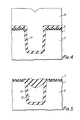
- a thin sacrificial layer 11 of polysilicon material (c.500 ⁇ ) is then deposited to cover the walls of the trench 9 and to cover the exposed surface of the nitride layer 5 — See Figure 3.
- the polysilicon layer 11 is then thermally oxidised. This step is performed at a temperature in the range 950° - 1050°C. Below this range of temperature, oxide viscosity would be low and would provide no means of relieving stress. Above this range, dopant redistribution effects would be unacceptable. This step of the method is also controlled to ensure that little if any of the adjacent wall silicon is oxidised, thereby to minimise any further dopant redistribution effects. During this step of the process the layer 11 expands providing a lighter density layer 13 of isolation oxide (c.1200 ⁇ ).
- the trench 9 is then infilled by depositing polysilicon material 15 — See Figure 4.
- the low defect density trench isolated structure can be used to electrically isolate MOS devices and Bipolar devices.
- the trench structure could also be used as a capacitor in an integrated circuit. Such a capacitor would have a large capacitance to chip area ratio enabling the packing density to remain high.
Landscapes
- Element Separation (AREA)
Applications Claiming Priority (2)
| Application Number | Priority Date | Filing Date | Title |
|---|---|---|---|
| GB08627666A GB2200794A (en) | 1986-11-19 | 1986-11-19 | Semiconductor device manufacture |
| GB8627666 | 1986-11-19 |
Publications (2)
| Publication Number | Publication Date |
|---|---|
| EP0278159A2 true EP0278159A2 (fr) | 1988-08-17 |
| EP0278159A3 EP0278159A3 (fr) | 1990-03-14 |
Family
ID=10607593
Family Applications (1)
| Application Number | Title | Priority Date | Filing Date |
|---|---|---|---|
| EP87310070A Withdrawn EP0278159A3 (fr) | 1986-11-19 | 1987-11-13 | Procédé pour la fabrication d'un dispositif semi-conducteur comportant une structure d'isolation |
Country Status (3)
| Country | Link |
|---|---|
| EP (1) | EP0278159A3 (fr) |
| JP (1) | JPS63288042A (fr) |
| GB (1) | GB2200794A (fr) |
Cited By (4)
| Publication number | Priority date | Publication date | Assignee | Title |
|---|---|---|---|---|
| EP0296754A3 (en) * | 1987-06-18 | 1990-08-01 | Kabushiki Kaisha Toshiba | Method of manufacturing a semiconductor device having a trench isolation region, and device manufactured by this method |
| EP0444836A3 (en) * | 1990-02-23 | 1991-11-06 | Sharp Kabushiki Kaisha | Process for forming semiconductor device isolation regions |
| EP0423722A3 (en) * | 1989-10-16 | 1993-01-13 | Kabushiki Kaisha Toshiba | Method of making complete dielectric isolation structure in semiconductor integrated circuit |
| EP0854510A3 (fr) * | 1996-12-26 | 1999-09-08 | Siemens Aktiengesellschaft | Enlèvement d'un masque pour la gravure d'un sillon d'une capacité DRAM |
Family Cites Families (7)
| Publication number | Priority date | Publication date | Assignee | Title |
|---|---|---|---|---|
| US4255207A (en) * | 1979-04-09 | 1981-03-10 | Harris Corporation | Fabrication of isolated regions for use in self-aligning device process utilizing selective oxidation |
| JPS5844735A (ja) * | 1981-09-11 | 1983-03-15 | Fujitsu Ltd | 半導体装置の製造方法 |
| JPS59135743A (ja) * | 1983-01-24 | 1984-08-04 | Hitachi Ltd | 半導体装置およびその製造方法 |
| JPS6083346A (ja) * | 1983-10-14 | 1985-05-11 | Hitachi Ltd | 半導体集積回路装置 |
| US4621414A (en) * | 1985-03-04 | 1986-11-11 | Advanced Micro Devices, Inc. | Method of making an isolation slot for integrated circuit structure |
| US4671970A (en) * | 1986-02-05 | 1987-06-09 | Ncr Corporation | Trench filling and planarization process |
| US4666556A (en) * | 1986-05-12 | 1987-05-19 | International Business Machines Corporation | Trench sidewall isolation by polysilicon oxidation |
-
1986
- 1986-11-19 GB GB08627666A patent/GB2200794A/en not_active Withdrawn
-
1987
- 1987-11-13 EP EP87310070A patent/EP0278159A3/fr not_active Withdrawn
- 1987-11-19 JP JP62293043A patent/JPS63288042A/ja active Pending
Cited By (5)
| Publication number | Priority date | Publication date | Assignee | Title |
|---|---|---|---|---|
| EP0296754A3 (en) * | 1987-06-18 | 1990-08-01 | Kabushiki Kaisha Toshiba | Method of manufacturing a semiconductor device having a trench isolation region, and device manufactured by this method |
| EP0423722A3 (en) * | 1989-10-16 | 1993-01-13 | Kabushiki Kaisha Toshiba | Method of making complete dielectric isolation structure in semiconductor integrated circuit |
| EP0444836A3 (en) * | 1990-02-23 | 1991-11-06 | Sharp Kabushiki Kaisha | Process for forming semiconductor device isolation regions |
| US5116779A (en) * | 1990-02-23 | 1992-05-26 | Sharp Kabushiki Kaisha | Process for forming semiconductor device isolation regions |
| EP0854510A3 (fr) * | 1996-12-26 | 1999-09-08 | Siemens Aktiengesellschaft | Enlèvement d'un masque pour la gravure d'un sillon d'une capacité DRAM |
Also Published As
| Publication number | Publication date |
|---|---|
| GB8627666D0 (en) | 1986-12-17 |
| EP0278159A3 (fr) | 1990-03-14 |
| JPS63288042A (ja) | 1988-11-25 |
| GB2200794A (en) | 1988-08-10 |
Similar Documents
| Publication | Publication Date | Title |
|---|---|---|
| US6174784B1 (en) | Technique for producing small islands of silicon on insulator | |
| US4755477A (en) | Overhang isolation technology | |
| EP0182998B1 (fr) | Procédé de préparation d'appuis métalliques entre un métal d'un premier niveau et des régions d'un semi-conducteur compatible avec des schémas à isolation à sillon profond rempli de polyimide | |
| KR930010986B1 (ko) | 반도체장치의 제조방법 | |
| EP0084635A2 (fr) | Procédé pour la formation d'une rainure large et profonde d'isolation remplie de diélectrique dans la surface rainure d'un substrat semi-conducteur en silicium | |
| US6140024A (en) | Remote plasma nitridation for contact etch stop | |
| US5470781A (en) | Method to reduce stress from trench structure on SOI wafer | |
| JPH01290236A (ja) | 幅の広いトレンチを平坦化する方法 | |
| US4708770A (en) | Planarized process for forming vias in silicon wafers | |
| US5882981A (en) | Mesa isolation Refill Process for Silicon on Insulator Technology Using Flowage Oxides as the Refill Material | |
| US6001705A (en) | Process for realizing trench structures | |
| JPH10335441A (ja) | 半導体装置の製造方法 | |
| US5989975A (en) | Method for manufacturing shallow trench isolation | |
| US6171929B1 (en) | Shallow trench isolator via non-critical chemical mechanical polishing | |
| US20020197822A1 (en) | Method of forming shallow trench isolation | |
| US5985725A (en) | Method for manufacturing dual gate oxide layer | |
| EP1198826A1 (fr) | Tranchees de semi-conducteurs et leur formation | |
| JP2000183152A (ja) | 半導体装置の製造方法 | |
| EP0140749B1 (fr) | Procédé de fabrication d'un dispositif semi-conducteur complémentaire à isolement diélectrique | |
| JP3049904B2 (ja) | 誘電体分離ウエハの製造方法 | |
| KR100245307B1 (ko) | 반도체 장치의 소자 분리방법 | |
| US6204547B1 (en) | Modified poly-buffered isolation | |
| GB2200794A (en) | Semiconductor device manufacture | |
| KR100392894B1 (ko) | 반도체 소자의 트렌치 형성 방법 | |
| US20030008474A1 (en) | Method of forming shallow trench isolation |
Legal Events
| Date | Code | Title | Description |
|---|---|---|---|
| PUAI | Public reference made under article 153(3) epc to a published international application that has entered the european phase |
Free format text: ORIGINAL CODE: 0009012 |
|
| AK | Designated contracting states |
Kind code of ref document: A2 Designated state(s): DE FR NL |
|
| PUAL | Search report despatched |
Free format text: ORIGINAL CODE: 0009013 |
|
| AK | Designated contracting states |
Kind code of ref document: A3 Designated state(s): DE FR NL |
|
| STAA | Information on the status of an ep patent application or granted ep patent |
Free format text: STATUS: THE APPLICATION IS DEEMED TO BE WITHDRAWN |
|
| 18D | Application deemed to be withdrawn |
Effective date: 19891201 |