EP0281740A2 - Speicher und deren Prüfung - Google Patents
Speicher und deren Prüfung Download PDFInfo
- Publication number
- EP0281740A2 EP0281740A2 EP88100944A EP88100944A EP0281740A2 EP 0281740 A2 EP0281740 A2 EP 0281740A2 EP 88100944 A EP88100944 A EP 88100944A EP 88100944 A EP88100944 A EP 88100944A EP 0281740 A2 EP0281740 A2 EP 0281740A2
- Authority
- EP
- European Patent Office
- Prior art keywords
- address
- test
- bit
- memory
- card
- Prior art date
- Legal status (The legal status is an assumption and is not a legal conclusion. Google has not performed a legal analysis and makes no representation as to the accuracy of the status listed.)
- Granted
Links
Images


Classifications
-
- G—PHYSICS
- G06—COMPUTING OR CALCULATING; COUNTING
- G06F—ELECTRIC DIGITAL DATA PROCESSING
- G06F11/00—Error detection; Error correction; Monitoring
-
- G—PHYSICS
- G11—INFORMATION STORAGE
- G11C—STATIC STORES
- G11C29/00—Checking stores for correct operation ; Subsequent repair; Testing stores during standby or offline operation
- G11C29/04—Detection or location of defective memory elements, e.g. cell constructio details, timing of test signals
- G11C29/08—Functional testing, e.g. testing during refresh, power-on self testing [POST] or distributed testing
- G11C29/12—Built-in arrangements for testing, e.g. built-in self testing [BIST] or interconnection details
- G11C29/38—Response verification devices
- G11C29/42—Response verification devices using error correcting codes [ECC] or parity check
-
- G—PHYSICS
- G11—INFORMATION STORAGE
- G11C—STATIC STORES
- G11C29/00—Checking stores for correct operation ; Subsequent repair; Testing stores during standby or offline operation
- G11C29/02—Detection or location of defective auxiliary circuits, e.g. defective refresh counters
-
- G—PHYSICS
- G11—INFORMATION STORAGE
- G11C—STATIC STORES
- G11C29/00—Checking stores for correct operation ; Subsequent repair; Testing stores during standby or offline operation
- G11C29/04—Detection or location of defective memory elements, e.g. cell constructio details, timing of test signals
- G11C29/08—Functional testing, e.g. testing during refresh, power-on self testing [POST] or distributed testing
- G11C29/10—Test algorithms, e.g. memory scan [MScan] algorithms; Test patterns, e.g. checkerboard patterns
-
- G—PHYSICS
- G11—INFORMATION STORAGE
- G11C—STATIC STORES
- G11C29/00—Checking stores for correct operation ; Subsequent repair; Testing stores during standby or offline operation
- G11C29/04—Detection or location of defective memory elements, e.g. cell constructio details, timing of test signals
- G11C29/08—Functional testing, e.g. testing during refresh, power-on self testing [POST] or distributed testing
- G11C29/12—Built-in arrangements for testing, e.g. built-in self testing [BIST] or interconnection details
- G11C29/18—Address generation devices; Devices for accessing memories, e.g. details of addressing circuits
-
- G—PHYSICS
- G06—COMPUTING OR CALCULATING; COUNTING
- G06F—ELECTRIC DIGITAL DATA PROCESSING
- G06F11/00—Error detection; Error correction; Monitoring
- G06F11/07—Responding to the occurrence of a fault, e.g. fault tolerance
- G06F11/0703—Error or fault processing not based on redundancy, i.e. by taking additional measures to deal with the error or fault not making use of redundancy in operation, in hardware, or in data representation
- G06F11/0751—Error or fault detection not based on redundancy
- G06F11/0754—Error or fault detection not based on redundancy by exceeding limits
- G06F11/076—Error or fault detection not based on redundancy by exceeding limits by exceeding a count or rate limit, e.g. word- or bit count limit
-
- G—PHYSICS
- G06—COMPUTING OR CALCULATING; COUNTING
- G06F—ELECTRIC DIGITAL DATA PROCESSING
- G06F11/00—Error detection; Error correction; Monitoring
- G06F11/07—Responding to the occurrence of a fault, e.g. fault tolerance
- G06F11/08—Error detection or correction by redundancy in data representation, e.g. by using checking codes
- G06F11/10—Adding special bits or symbols to the coded information, e.g. parity check, casting out 9's or 11's
- G06F11/1008—Adding special bits or symbols to the coded information, e.g. parity check, casting out 9's or 11's in individual solid state devices
- G06F11/1048—Adding special bits or symbols to the coded information, e.g. parity check, casting out 9's or 11's in individual solid state devices using arrangements adapted for a specific error detection or correction feature
- G06F11/1052—Bypassing or disabling error detection or correction
Definitions
- the present invention relates to memories and the testing thereof and seeks to provide an efficient test for address line failures in a large scale storage system of an information handling system and equally a storage system having such a test built into it.
- the present invention separates addressing mechanism testing from other aspects of testing the memory and provides a system operated memory test comprising testing address lines independently of other memory aspects by systematically testing one memory location per address line relative to a datum location, where the address of the location associated with a particular address line is that of the datum location but with the bit of the particular address line inverted, by writing a data pattern into the datum location and a divergent, preferably the inverted form, data pattern into the address line associated location, reading out the two patterns with the error mechanisms, if any, disabled and comparing the two accessed patterns, the procedure being repeated with the patterns reversed.
- test data pattern As to the test data pattern, it is pointed out that with double bit correction provided by the error correcting code logic in a card organised memory, a number of bits can be corrected on a card or a larger number of bits can be corrected on a card pair, where the larger number of bits is somewhat less than double the number of bits which can be corrected on a single card.
- the address test in accordance with the present invention then produces a pattern that will create a difference greater than that larger number of bits between the data stored in a storage location under test and any address that could be accessed by an address line failure. The test predicts the effect of an address line failure external to the array modules and internal to a card pair and then tests to see if a failure has occurred.
- the address test does not declare an address failure until a predetermined number of bit failures on a card is found.
- the test is valid for single and multiple address line failures. Since only one address bit is changed for each path through the test other failing address lines will not be detected until the path with those failing address bits are tested. Thus, even with multiple address line failure the two addresses that are stored to and fetched from are the only one address bit apart.
- the present invention also provides a memory system and equally a data processing system having such a test built into it.
- U.S. Patent 4,369,511 describes a semi-conductor memory test system which reads a memory under test at an address generated by a pattern generator and compares data read data from the address with expected data. A block mask memory is read by a portion of the address and the comparing operation of the comparator is inhibited by block mask data read from the block mask memory.
- the method for memory testing according to the patent is significantly different from the present invention in that the patent requires a comparison of data read from a memory with data generated and fed through a test memory 22 and compared in comparator 19.
- data is stored in address locations being one bit different and the data is read from the two locations and compared.
- U.S. Patent 4,404,519 provides method and apparatus for testing data stored in a memory array embedded in a large scale integrated circuit. The method and apparatus of the patent do not describe or suggest the method for testing address lines in accordance with the present invention.
- U.S. Patent 4,429,389 teaches a test pattern address generator which generates specialised address patterns in which an address generator is complimented and then incremented on a series of increment-compliment actions so that all combinations of row and column drivers in the integrated circuit memory under test are exercised.
- each address line bit is separately tested by a two-pass test in which divergent data is stored into the address under test and the address into which data would be stored if there was an address line failure for the address bit under test.
- U.S. Patent 4,559,626 teaches a test apparatus for testing memories which includes an internal memory into which data patterns are stored for comparison with data patterns stored in a memory under test. The patterns are then read from the internal memory of the tester and the memory under test and compared.
- each address line bit is separately tested by a two-pass test in which divergent data is stored into the address under test and the address into which data would be stored if there was an address line failure for the address bit under test.
- test of the present invention is a simple and efficient method which provides unique failure information for any address bit failure in the memory system.
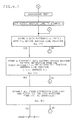
- FIG. 1 is a simple block diagram that shows processor 10 which is connected to storage system 12 by data, address,error and control lines 14.
- processor 10 and storage system 12 may be implemented in many ways by systems that are currently available from many hardware suppliers such as IBM Corporation.
- the processor could be an IBM system 370 processor with its own internal storage system, or an IBM 3880 Model 23 with cache storage system 12 or storage sub-system such as might be used to control direct access storage devices (DASD).
- DASD direct access storage devices
- the time required to test a large memory is very prohibitive.
- the projected time required to test a 256 megabyte storage system will be 1 hour 48 minutes and 32 seconds.
- the method of the present invention is to remove as much dependency on the data as possible when testing the address lines. With this method, the testing of the address lines can be accomplished in as little as one second.
- a separate data test must be performed, but such a data test can be run concurrently with normal system operation.
- Card 16 will be described in which the address lines between the buffers 20, 22, and 24 and the memory arrays 26 a, b, c, and d, are tested.
- Card 16 also includes a set of bi-directional drivers 28 for handling the transmission of data on and off the card.
- Control lines are connected as inputs to control block 18 which controls the read, write, enable, test, card select and addressing of the arrays 26 a, b, c, d inclusive on card 16.
- Fig. 3 shows a typical address bus structure for a large memory sub-system might include 24 bits wherein 20 bits address locations unique to each card and 4 bits provide card select. Thus, there would be a possibility of 16 cards each card having one million addressable locations.
- FIG. 3 The address bus structure of Fig. 3 is shown merely for illustration of a typical addressing scheme for a large scale memory and is not intended to in any way limit the application of the present invention.
- an appropriate request is sent to the memory control processor 10 in the memory subsystem.
- the control processor 10 then begins the address test by setting a first bit in the address to a one as the active address line.
- a first data pattern such as an all zeros data pattern is then stored into that active address line position.
- an all ones pattern might be stored into address zero where the active address line position and the bit under test is the low order bit of the address.
- the structure of the address on the address bus the low order address bit position would be identified as bit 23.
- the active address line position would be address 1 and the inactive address line position would be address 0.
- the normal hardware error correction is performed.
- the test ends with an isolation code indicating the cause of the error is generated.
- a predetermined number of acceptable data bit errors is set that the system can detect and correct. If the number of data bits in any particular compared exceeds that number, an address line failure is indicated and the test is ended with an appropriate error code. In a preferred embodiment of the present invention, six errors per card may be accepted before address line failure is indicated.
- test increments to the next bit in the address as the active line and the above steps are repeated. These steps are repeated until all of the address bits in the storage address have been tested for a particular card. It should be noted, that when a next card is to be tested, there will be a change in the card select bits which are at the high order at the address and each of the 20 low order address bits must be again tested as above for each card in the system.
- a second pass is then conducted in which the active address line is again set to the low order address bit and the second data pattern such as all zeros is stored into the inactive address line position address zero and the data pattern that was stored into the inactive address line position for the first pass is now stored into the active address line position such as storing all ones in address one.
- the low order address bit referred to is bit 23 as shown in Fig. 3.
- hardware error checks such as parity are active to ensure that no unrelated error masks the errors which may occur as a result of the test being conducted.
- the data stored in the two addresses are then read and compared bit by bit and the number of error bits are counted to determine if the predetermined number of acceptable and correctable errors has been exceeded. If such number of error bits has been exceeded, the test is ended indicating an address line failure error code.
- next address bit is then made the active address bit position and the second pass is conducted for such next bit position in the address.
- each location used could have its comparison performed with one order of the patterns before any comparison is performed with the patterns reversed. This could mean that the datum location only needed writing twice, one for each order of the patterns.
- card select lines at the high end of the address and, obviously, these could be module or sub-unit select lines depending on the memory structure, should be verified by separate select test prior to the address line test which is the subject of the present invention.
- the number of acceptable data bit errors is dependent on the error correction capability of the storage system and the number of spare memory locations per card/module/sub-unit, as described, the number of spare chips on each memory card. For example, if double bit correction is provided by a storage system, and each memory card has one spare chip and one bit is read from each chip, then the number of acceptable data errors is three.
- the address line test of the present invention is only valid on storage systems in which each address line partially selects more memory locations than the number of acceptable data bit errors as discussed above.
Landscapes
- Engineering & Computer Science (AREA)
- Theoretical Computer Science (AREA)
- Techniques For Improving Reliability Of Storages (AREA)
- General Engineering & Computer Science (AREA)
- General Physics & Mathematics (AREA)
- Physics & Mathematics (AREA)
- Quality & Reliability (AREA)
- For Increasing The Reliability Of Semiconductor Memories (AREA)
- Tests Of Electronic Circuits (AREA)
- Memory System Of A Hierarchy Structure (AREA)
- Debugging And Monitoring (AREA)
- Credit Cards Or The Like (AREA)
- Slot Machines And Peripheral Devices (AREA)
Priority Applications (1)
| Application Number | Priority Date | Filing Date | Title |
|---|---|---|---|
| AT88100944T ATE83331T1 (de) | 1987-02-13 | 1988-01-22 | Speicher und deren pruefung. |
Applications Claiming Priority (2)
| Application Number | Priority Date | Filing Date | Title |
|---|---|---|---|
| US07/014,749 US4891811A (en) | 1987-02-13 | 1987-02-13 | Efficient address test for large memories |
| US14749 | 1987-02-13 |
Publications (3)
| Publication Number | Publication Date |
|---|---|
| EP0281740A2 true EP0281740A2 (de) | 1988-09-14 |
| EP0281740A3 EP0281740A3 (en) | 1990-05-09 |
| EP0281740B1 EP0281740B1 (de) | 1992-12-09 |
Family
ID=21767473
Family Applications (1)
| Application Number | Title | Priority Date | Filing Date |
|---|---|---|---|
| EP88100944A Expired - Lifetime EP0281740B1 (de) | 1987-02-13 | 1988-01-22 | Speicher und deren Prüfung |
Country Status (14)
| Country | Link |
|---|---|
| US (1) | US4891811A (de) |
| EP (1) | EP0281740B1 (de) |
| JP (1) | JP2519286B2 (de) |
| KR (1) | KR920001104B1 (de) |
| CN (1) | CN1008848B (de) |
| AT (1) | ATE83331T1 (de) |
| AU (1) | AU597140B2 (de) |
| BR (1) | BR8800244A (de) |
| CA (1) | CA1291269C (de) |
| DE (1) | DE3876459T2 (de) |
| ES (1) | ES2036223T3 (de) |
| GB (1) | GB2201016B (de) |
| HK (1) | HK35392A (de) |
| SG (1) | SG110891G (de) |
Cited By (1)
| Publication number | Priority date | Publication date | Assignee | Title |
|---|---|---|---|---|
| US12332781B2 (en) | 2023-09-19 | 2025-06-17 | Bae Systems Information And Electronic Systems Integration Inc. | Verification process for bit spreading error resistant memory system |
Families Citing this family (21)
| Publication number | Priority date | Publication date | Assignee | Title |
|---|---|---|---|---|
| US5073891A (en) * | 1990-02-14 | 1991-12-17 | Intel Corporation | Method and apparatus for testing memory |
| US5555249A (en) * | 1991-09-18 | 1996-09-10 | Ncr Corporation | Non-destructive memory testing in computers |
| US5469443A (en) * | 1993-10-01 | 1995-11-21 | Hal Computer Systems, Inc. | Method and apparatus for testing random access memory |
| US5479413A (en) * | 1994-06-06 | 1995-12-26 | Digital Equipment Corporation | Method for testing large memory arrays during system initialization |
| US5539878A (en) * | 1995-06-16 | 1996-07-23 | Elonex Technologies, Inc. | Parallel testing of CPU cache and instruction units |
| US20020091965A1 (en) * | 2000-12-22 | 2002-07-11 | Mark Moshayedi | System and method for early detection of impending failure of a data storage system |
| US6842867B2 (en) | 2001-01-26 | 2005-01-11 | Dell Products L.P. | System and method for identifying memory modules having a failing or defective address |
| US7308621B2 (en) | 2002-04-30 | 2007-12-11 | International Business Machines Corporation | Testing of ECC memories |
| US7149941B2 (en) | 2002-04-30 | 2006-12-12 | International Business Machines Corporation | Optimized ECC/redundancy fault recovery |
| US7085973B1 (en) * | 2002-07-09 | 2006-08-01 | Xilinx, Inc. | Testing address lines of a memory controller |
| JP4299558B2 (ja) * | 2003-03-17 | 2009-07-22 | 株式会社ルネサステクノロジ | 情報記憶装置および情報処理システム |
| KR20060014057A (ko) * | 2003-05-22 | 2006-02-14 | 코닌클리즈케 필립스 일렉트로닉스 엔.브이. | 전자 회로 테스트 방법 및 장치 |
| US8230275B2 (en) * | 2005-05-26 | 2012-07-24 | Hewlett-Packard Development Company, L.P. | Use of parity bits to detect memory installation defects |
| CN101310343B (zh) * | 2005-11-14 | 2014-04-30 | 三菱电机株式会社 | 存储器诊断装置 |
| US7609561B2 (en) * | 2006-01-18 | 2009-10-27 | Apple Inc. | Disabling faulty flash memory dies |
| CN100445963C (zh) * | 2007-02-15 | 2008-12-24 | 华为技术有限公司 | 一种实现高可靠性空闲链表的方法及装置 |
| EP2063432B1 (de) * | 2007-11-15 | 2012-08-29 | Grundfos Management A/S | Verfahren zum Prüfen eines Arbeitsspeichers |
| DE102010027287A1 (de) * | 2010-07-16 | 2012-01-19 | Siemens Aktiengesellschaft | Verfahren und Vorrichtung zum prüfen eines Hauptspeichers eines Prozessors |
| US9189313B2 (en) * | 2012-08-27 | 2015-11-17 | Kabushiki Kaisha Toshiba | Memory system having NAND-type flash memory and memory controller with shift read controller and threshold voltage comparison module |
| CN104425040A (zh) * | 2013-08-23 | 2015-03-18 | 辉达公司 | 用于测试存储器的方法和系统 |
| CN113777911B (zh) * | 2021-10-09 | 2023-06-02 | 中国北方车辆研究所 | 一种基于地址编码的控制器复合防错方法 |
Family Cites Families (17)
| Publication number | Priority date | Publication date | Assignee | Title |
|---|---|---|---|---|
| US3727039A (en) * | 1971-08-02 | 1973-04-10 | Ibm | Single select line storage system address check |
| JPS5138570B2 (de) * | 1971-10-13 | 1976-10-22 | ||
| NL7416755A (nl) * | 1974-12-23 | 1976-06-25 | Philips Nv | Werkwijze en inrichting voor het testen van een digitaal geheugen. |
| US4100403A (en) * | 1977-04-25 | 1978-07-11 | International Business Machines Corporation | Method and means for discriminating between systematic and noise-induced error in data extracted from word organized memory arrays |
| JPS5634198A (en) * | 1979-08-27 | 1981-04-06 | Nippon Telegr & Teleph Corp <Ntt> | Releaving method of deficient bit of semiconductor memory |
| JPS5651678A (en) * | 1979-10-03 | 1981-05-09 | Nippon Telegr & Teleph Corp <Ntt> | Testing method for memory element and pattern generator for test |
| DD148268A1 (de) * | 1979-12-21 | 1981-05-13 | Haupt Wolf Dieter | Schaltungsanordnung zur blockweisen pruefung von hauptspeichern |
| JPS6019080B2 (ja) * | 1980-10-17 | 1985-05-14 | 富士通株式会社 | 記憶装置のチェック方法 |
| US4429389A (en) * | 1981-05-26 | 1984-01-31 | Burroughs Corporation | Test pattern address generator |
| EP0088916B1 (de) * | 1982-03-15 | 1985-11-21 | Siemens-Albis Aktiengesellschaft | Schaltungsanordnung zum Prüfen von elektrischen, insbesondere elektronischen Einrichtungen |
| JPS59180898A (ja) * | 1983-03-31 | 1984-10-15 | Hitachi Ltd | 不良ビット救済方法 |
| GB8401806D0 (en) * | 1984-01-24 | 1984-02-29 | Int Computers Ltd | Data storage apparatus |
| JPS61137300A (ja) * | 1984-12-06 | 1986-06-24 | Sony Tektronix Corp | メモリ検査方法 |
| US4757503A (en) * | 1985-01-18 | 1988-07-12 | The University Of Michigan | Self-testing dynamic ram |
| US4715034A (en) * | 1985-03-04 | 1987-12-22 | John Fluke Mfg. Co., Inc. | Method of and system for fast functional testing of random access memories |
| JPS61278992A (ja) * | 1985-06-04 | 1986-12-09 | Toppan Moore Co Ltd | 故障検査機能を備えたicカ−ド |
| US4686456A (en) * | 1985-06-18 | 1987-08-11 | Kabushiki Kaisha Toshiba | Memory test circuit |
-
1987
- 1987-02-13 US US07/014,749 patent/US4891811A/en not_active Expired - Fee Related
- 1987-08-17 GB GB8719405A patent/GB2201016B/en not_active Expired - Lifetime
-
1988
- 1988-01-07 CA CA000556026A patent/CA1291269C/en not_active Expired - Lifetime
- 1988-01-18 AU AU10356/88A patent/AU597140B2/en not_active Ceased
- 1988-01-22 EP EP88100944A patent/EP0281740B1/de not_active Expired - Lifetime
- 1988-01-22 DE DE8888100944T patent/DE3876459T2/de not_active Expired - Fee Related
- 1988-01-22 AT AT88100944T patent/ATE83331T1/de not_active IP Right Cessation
- 1988-01-22 ES ES198888100944T patent/ES2036223T3/es not_active Expired - Lifetime
- 1988-01-25 BR BR8800244A patent/BR8800244A/pt unknown
- 1988-02-01 CN CN88100490A patent/CN1008848B/zh not_active Expired
- 1988-02-10 JP JP63027818A patent/JP2519286B2/ja not_active Expired - Lifetime
- 1988-02-12 KR KR1019880001348A patent/KR920001104B1/ko not_active Expired
-
1991
- 1991-12-31 SG SG1108/91A patent/SG110891G/en unknown
-
1992
- 1992-05-21 HK HK353/92A patent/HK35392A/xx unknown
Cited By (1)
| Publication number | Priority date | Publication date | Assignee | Title |
|---|---|---|---|---|
| US12332781B2 (en) | 2023-09-19 | 2025-06-17 | Bae Systems Information And Electronic Systems Integration Inc. | Verification process for bit spreading error resistant memory system |
Also Published As
| Publication number | Publication date |
|---|---|
| BR8800244A (pt) | 1988-08-30 |
| SG110891G (en) | 1992-02-14 |
| CN88100490A (zh) | 1988-08-24 |
| DE3876459T2 (de) | 1993-06-09 |
| GB2201016A (en) | 1988-08-17 |
| DE3876459D1 (de) | 1993-01-21 |
| CA1291269C (en) | 1991-10-22 |
| JP2519286B2 (ja) | 1996-07-31 |
| KR920001104B1 (ko) | 1992-02-01 |
| HK35392A (en) | 1992-05-29 |
| KR880010362A (ko) | 1988-10-08 |
| US4891811A (en) | 1990-01-02 |
| JPS63202000A (ja) | 1988-08-22 |
| CN1008848B (zh) | 1990-07-18 |
| AU597140B2 (en) | 1990-05-24 |
| ES2036223T3 (es) | 1993-05-16 |
| ATE83331T1 (de) | 1992-12-15 |
| EP0281740B1 (de) | 1992-12-09 |
| GB2201016B (en) | 1991-03-13 |
| GB8719405D0 (en) | 1987-09-23 |
| AU1035688A (en) | 1988-08-18 |
| EP0281740A3 (en) | 1990-05-09 |
Similar Documents
| Publication | Publication Date | Title |
|---|---|---|
| EP0281740B1 (de) | Speicher und deren Prüfung | |
| US5267242A (en) | Method and apparatus for substituting spare memory chip for malfunctioning memory chip with scrubbing | |
| US5659678A (en) | Fault tolerant memory | |
| EP0136443B1 (de) | Speicherkorrektursystem unter Verwendung von Reservematrizen | |
| EP0030612B1 (de) | Verfahren zur Doppelfehlerkorrektur in einem Datenspeichergerät und Datenspeichergerät | |
| US6397357B1 (en) | Method of testing detection and correction capabilities of ECC memory controller | |
| EP0494547A2 (de) | Fehlerabbildungsgerät für Computerspeicher | |
| JPH10283274A (ja) | メモリをテストするための方法および装置 | |
| US5612965A (en) | Multiple memory bit/chip failure detection | |
| US5357521A (en) | Address sensitive memory testing | |
| KR100609343B1 (ko) | 컴퓨터 메모리 시스템에서의 멀티-비트 에러 보호를 위한시스템 및 방법 | |
| US5822513A (en) | Method and apparatus for detecting stale write data | |
| US7418636B2 (en) | Addressing error and address detection systems and methods | |
| US7222271B2 (en) | Method for repairing hardware faults in memory chips | |
| US7464309B2 (en) | Method and apparatus for testing semiconductor memory device and related testing methods | |
| EP0366757B1 (de) | Verfahren und vorrichtung zum speicherselbsttest | |
| US6279129B1 (en) | Configuration of memory cells and method of checking the operation of memory cells | |
| US6795938B2 (en) | Memory access controller with response faking | |
| JPH05216778A (ja) | メモリサブシステム | |
| EP0652568A1 (de) | Prüfgerät für Speicherkarte | |
| EP0442616A2 (de) | Verfahren zur Rechnerspeicherplatzprüfung | |
| JP3071846B2 (ja) | パリティーエラー検出方法及びパリティーエラー検出回路 | |
| JPH10105421A (ja) | Aramメモリチップを用いてsimmメモリモジュールを製作し試験する装置 | |
| EP0533375A2 (de) | Rechnersystem mit Speicherprüfmitteln | |
| JPH04101253A (ja) | メモリのecc回路の動作試験方式 |
Legal Events
| Date | Code | Title | Description |
|---|---|---|---|
| PUAI | Public reference made under article 153(3) epc to a published international application that has entered the european phase |
Free format text: ORIGINAL CODE: 0009012 |
|
| AK | Designated contracting states |
Kind code of ref document: A2 Designated state(s): AT BE CH DE ES FR GB IT LI NL SE |
|
| 17P | Request for examination filed |
Effective date: 19881130 |
|
| PUAL | Search report despatched |
Free format text: ORIGINAL CODE: 0009013 |
|
| AK | Designated contracting states |
Kind code of ref document: A3 Designated state(s): AT BE CH DE ES FR GB IT LI NL SE |
|
| 17Q | First examination report despatched |
Effective date: 19920403 |
|
| GRAA | (expected) grant |
Free format text: ORIGINAL CODE: 0009210 |
|
| AK | Designated contracting states |
Kind code of ref document: B1 Designated state(s): AT BE CH DE ES FR GB IT LI NL SE |
|
| PG25 | Lapsed in a contracting state [announced via postgrant information from national office to epo] |
Ref country code: NL Effective date: 19921209 Ref country code: BE Effective date: 19921209 |
|
| REF | Corresponds to: |
Ref document number: 83331 Country of ref document: AT Date of ref document: 19921215 Kind code of ref document: T |
|
| ET | Fr: translation filed | ||
| REF | Corresponds to: |
Ref document number: 3876459 Country of ref document: DE Date of ref document: 19930121 |
|
| ITF | It: translation for a ep patent filed | ||
| REG | Reference to a national code |
Ref country code: ES Ref legal event code: FG2A Ref document number: 2036223 Country of ref document: ES Kind code of ref document: T3 |
|
| NLV1 | Nl: lapsed or annulled due to failure to fulfill the requirements of art. 29p and 29m of the patents act | ||
| PLBE | No opposition filed within time limit |
Free format text: ORIGINAL CODE: 0009261 |
|
| STAA | Information on the status of an ep patent application or granted ep patent |
Free format text: STATUS: NO OPPOSITION FILED WITHIN TIME LIMIT |
|
| 26N | No opposition filed | ||
| EAL | Se: european patent in force in sweden |
Ref document number: 88100944.3 |
|
| PGFP | Annual fee paid to national office [announced via postgrant information from national office to epo] |
Ref country code: FR Payment date: 19960103 Year of fee payment: 9 |
|
| PGFP | Annual fee paid to national office [announced via postgrant information from national office to epo] |
Ref country code: SE Payment date: 19960104 Year of fee payment: 9 |
|
| PGFP | Annual fee paid to national office [announced via postgrant information from national office to epo] |
Ref country code: ES Payment date: 19960123 Year of fee payment: 9 |
|
| PGFP | Annual fee paid to national office [announced via postgrant information from national office to epo] |
Ref country code: CH Payment date: 19960426 Year of fee payment: 9 |
|
| PG25 | Lapsed in a contracting state [announced via postgrant information from national office to epo] |
Ref country code: SE Effective date: 19970123 Ref country code: ES Free format text: LAPSE BECAUSE OF NON-PAYMENT OF DUE FEES Effective date: 19970123 |
|
| PGFP | Annual fee paid to national office [announced via postgrant information from national office to epo] |
Ref country code: DE Payment date: 19970128 Year of fee payment: 10 |
|
| PGFP | Annual fee paid to national office [announced via postgrant information from national office to epo] |
Ref country code: AT Payment date: 19970130 Year of fee payment: 10 |
|
| PG25 | Lapsed in a contracting state [announced via postgrant information from national office to epo] |
Ref country code: LI Effective date: 19970131 Ref country code: CH Effective date: 19970131 |
|
| REG | Reference to a national code |
Ref country code: CH Ref legal event code: PL |
|
| PG25 | Lapsed in a contracting state [announced via postgrant information from national office to epo] |
Ref country code: FR Effective date: 19970930 |
|
| EUG | Se: european patent has lapsed |
Ref document number: 88100944.3 |
|
| REG | Reference to a national code |
Ref country code: FR Ref legal event code: ST |
|
| PG25 | Lapsed in a contracting state [announced via postgrant information from national office to epo] |
Ref country code: AT Free format text: LAPSE BECAUSE OF NON-PAYMENT OF DUE FEES Effective date: 19980122 |
|
| PG25 | Lapsed in a contracting state [announced via postgrant information from national office to epo] |
Ref country code: DE Free format text: LAPSE BECAUSE OF NON-PAYMENT OF DUE FEES Effective date: 19981001 |
|
| REG | Reference to a national code |
Ref country code: ES Ref legal event code: FD2A Effective date: 19990503 |
|
| REG | Reference to a national code |
Ref country code: GB Ref legal event code: IF02 |
|
| PGFP | Annual fee paid to national office [announced via postgrant information from national office to epo] |
Ref country code: GB Payment date: 20020102 Year of fee payment: 15 |
|
| PG25 | Lapsed in a contracting state [announced via postgrant information from national office to epo] |
Ref country code: GB Free format text: LAPSE BECAUSE OF NON-PAYMENT OF DUE FEES Effective date: 20030122 |
|
| GBPC | Gb: european patent ceased through non-payment of renewal fee | ||
| PG25 | Lapsed in a contracting state [announced via postgrant information from national office to epo] |
Ref country code: IT Free format text: LAPSE BECAUSE OF NON-PAYMENT OF DUE FEES;WARNING: LAPSES OF ITALIAN PATENTS WITH EFFECTIVE DATE BEFORE 2007 MAY HAVE OCCURRED AT ANY TIME BEFORE 2007. THE CORRECT EFFECTIVE DATE MAY BE DIFFERENT FROM THE ONE RECORDED. Effective date: 20050122 |