EP0281889A2 - Circuit de mémoire avec contrôle de la sortie de données - Google Patents
Circuit de mémoire avec contrôle de la sortie de données Download PDFInfo
- Publication number
- EP0281889A2 EP0281889A2 EP88103020A EP88103020A EP0281889A2 EP 0281889 A2 EP0281889 A2 EP 0281889A2 EP 88103020 A EP88103020 A EP 88103020A EP 88103020 A EP88103020 A EP 88103020A EP 0281889 A2 EP0281889 A2 EP 0281889A2
- Authority
- EP
- European Patent Office
- Prior art keywords
- circuit
- signal
- sense amplifier
- control signal
- output
- Prior art date
- Legal status (The legal status is an assumption and is not a legal conclusion. Google has not performed a legal analysis and makes no representation as to the accuracy of the status listed.)
- Withdrawn
Links
Images


Classifications
-
- G—PHYSICS
- G11—INFORMATION STORAGE
- G11C—STATIC STORES
- G11C8/00—Arrangements for selecting an address in a digital store
- G11C8/18—Address timing or clocking circuits; Address control signal generation or management, e.g. for row address strobe [RAS] or column address strobe [CAS] signals
-
- G—PHYSICS
- G11—INFORMATION STORAGE
- G11C—STATIC STORES
- G11C2207/00—Indexing scheme relating to arrangements for writing information into, or reading information out from, a digital store
- G11C2207/06—Sense amplifier related aspects
- G11C2207/061—Sense amplifier enabled by a address transition detection related control signal
Definitions
- the present invention relates to a memory circuit and more particularly to a static type memory circuit provided with an internal control signal generator for generating timing signals when at least one input signal changes in level.
- the internally synchronous type memory has a timing signal generater which generates a series of timing signals for controlling the respective functional circuits in the memory upon each change in at least one input signal such as address input signals.
- the pulse word architecture suppresses undesired charge and discharge currents in bit lines and in data bus lines as well as DC current of the sense amplifier, and is effective for decreasing the consumption of electric power.
- the above-mentioned conventional memory circuit has defects as described below.
- One of the nuisances involved in the memory circuit is a change in the power source voltage Vcc and in the ground potential GND accompanying a change in the operation current in the memory circuit.
- the output transistor usually charges and discharges a capacity of from several tens to several hundreds of picofarads, and is generally designed to exhibit a large transistor ability. Therefore, the switching current of the output transistor at the time of reading operation causes the power source voltage Vcc and ground potential GND to change most greatly among other circuit operations.
- the input stage of an address buffer may sense a change in the power supply voltage Vcc and in the ground potential GND caused by this change as the change in the input potential itself applied thereto, whereby the address buffer starts to operate. That is, the potential change is added to the input voltage of the address buffer, and the input level loses its actual, absolute level which is detrimental to the characteristics. Moreover, a great change in the potential makes it difficult to satisfy the specifications of the input level.
- the memory circuit comprises a memory cell array, a sense amplifier, a latch circuit for operatively holding the output of the sense amplifier and a control signal generator for generating when it least one address input signal is changed, a first control signal for precharging the memory cell array and a second control signal for enabling the sense amplifier and is featured by a transferring circuit for transferring the output of the sense amplifier to the latch circuit only when the second control signal is present and the first control signal is not present.
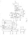
- the memory circuit comprises a memory cell array 13 having a plurality of static type memory cells MC, a plurality of pairs of bit lines DL, DL and a plurality of word lines WL.
- Each pair of bit lines DL and D L are provided with P-channel precharge transistors Q, to Q 3 controlled by a first timing signal OS1 for resetting.
- a word decoder 11 receives row address signals A 0 -A i to select one of the word lines WL.
- a column decoder 12 receives column address signals A i+1 -A n to render a selected pair of column selection gates QY, QY conductive so that the selected pair of bit lines are electrically connected to a pair of data bus lines DB, DB .
- the pair of bus lines DB, DB are connected to a pair of input nodes of a differential type sense amplifier 14 which is reset by the first timing signal OS1 and enabled by a second timing signal OS2.
- the data bus lines are provided with P-channel transistors Q 4 -Q 6 .
- An output node of the sense amplifier 14 is connected to an input node of a latch circuit 15 via a read data line RB.
- the latch circuit 15 takes the state of RB thereinto in response to a third timing signal OS3.
- a timing signal generator 17 receives each of address signals A o -An and generates the low-going pulse of the first timing signal OS1 whenever at least one of the address input signals A o -A n is changed in level and further generates the positive-going pulse of the second timing signal OS2 after the generation of OS1.
- the signal OS1 is used as a control signal for precharging and equalizing the bit lines and the data bus lines DB, DB before the reading operation is started.
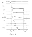
- the signal OS1 is a one-shot signal having a narrower pulse width to obtain a higher operation speed, as shown in Fig. 3A.
- the signal OS2, on the other hand, is used for determining a period for selecting the word line and for determining a period for activating the sense amplifier 14. Therefore, the signal OS2 has a width longer than a period in which the read-out data is transmitted to the latch circuit 15, as shown in Fig. 3A.
- a change in the address signal (one of A 0 -A n ) gives rise to the generation of the signals OS1 and OS2.
- the signal OS1 assumes the "L" level at a mount T 1a , the P-channel MOS transistors Q 4 to Q 6 are rendered conductive to precharge the data bus lines DB and D B to the Vcc level.
- the latch circuit 15 is enabled by the signal OS3, which will be described later in detail, and the data on the line RB is transferred to the latch circuit 15 and latched therein.
- the latch circuit output LB is transmitted to the output circuit 16 and the read-out data finally appears on the memory circuit output OUT so that the reading operation is completed.
- the sense amplifier 14 stays no more in the active condition. Therefore, no DC current flows into the sense amplifier 14 after the moment T 38 , contributing the saving the consumption of electric power.
- the sense amplifier output RB assumes an indefinite level since the sense amplifier is no more in the active condition. Since the signal OS3 assumes the "L" level, however, the latch circuit 15 continues to hold the read-out data.
- the sense amplifier 14 is composed of P-channel MOS transistors Q, and Q 8 serving as load elements, and Q9 for equalization of a pair of output nodes, N-channel MOS transistors Q, o , Q,, serving as differential input transistors, and Q 12 as a current source for enabling the amplifier 14.
- the transistor Q 9 is made conductive in response to "L" (low) level of the signal OS1 to set the sense amplifier in a reset, equalized state.
- the transistor Q 12 is made conductive in response to "H" (high) level of the signal OS2 thereby to enable the sense amplifier 14.
- the latch circuit 15 includes inverters IV2 and IV3 forming a known flip-flop, IV5 serving as an output inverter, and a CMOS transfer gate made of an N-channel MOS transistor Q 13 and a P-channel MOS transistor Q 14 for writing the sense amplifier output RB to the flip-flop (IV2, IV3) in response to "H" level of a control signal OS3 which is generated from an output an inverter IV4 whose input is connected to an output of a NAND gate AG1 receiving the signals OS1 and OS2.
- control signal generator 17 An example of the control signal generator 17 is shown in Fig. 2.
- An address change detect circuit ATD receives a buffered address signal of an address input signal A via inverter circuits A 41 and A1 2 and includes inverter circuits A 47 and A 47 which constitute a delay circuit with a capacitor C 41 , a NAND circuit B 41 , a NOR circuit D 41 , an inverter A 49 and a NOR circuit D 42 .
- Inverters A 43 to A 46 are for generating true and complementary internal address signals A ; ' and A i ' of the address input signal A i .
- the internal address signals A;' and A i ' are usually applied to the address decoders such as those 11 and 12 in a known way.
- the address change detect circuit ATD produces an upwardly directed output ⁇ i of a pulse width defined by the delay time of the delay circuit made by the inverter circuits A 47 , A 48 and by the capacitor C,,.
- the output ⁇ i of the address change detect circuit is sent to one of input terminals of a NOR circuit D 43 which receives outputs ⁇ 0 - ⁇ i+1 , ⁇ i+1 - ⁇ n of other address change detection circuits (not shown) of other address input signals A o -An.
- the first control signal OS1 is applied to an input of an inverter circuit A 4A whose output is applied to cascaded-connected inverters A 4B and A 4c .
- the inverters A 4A -A 4c form a pulse-width change circuit for generating the second control signal OS2.
- the pulse-width change circuit makes the second control signal OS2 at the "H” (high) level after a first delay time from the change of OS1 to the "L" level from the "H” level and makes the second control signal OS2 at the "L” level after a second delay time longer than the first delay time from the time point when the first control signal OS1 is changed to the "H" level from the "L” level.
- the inverter circuit A 4A produces a large current capacity when the output changes from the "H” level to the “L” level and sets a small current capacity when the output changes from the "L” level to the “H” level. That is, when the signal OS1 rises, the moment at which the signal OS2 breaks is determined by a delay time determined by a capacity C 42 that is connected to the inverter circuit A4A.
- the signal OS1 is used as a control signal for precharging and equalizing the bit lines and data bus lines before the reading operation is started, as mentioned above. That is, it is urged to obtain a one-shot signal having a narrower pulse width to obtain a higher operation speed.
- the signal OS2, on the other hand, is used for determining a period for selecting the word line and for determining a period for activating the sense amplifier. Therefore, the pulse signal have a width longer than a period in which the read-out data is transmitted to the latch circuit.
- One of the nuisances involved in using the memory circuit is a change in the power source voltage Vcc and in the ground potential GND accompanying a change in the operation current in the memory circuit.
- the output transistor usually charges and discharges a capacity of from several tens to several hundreds of picofarads and is generally designed to exhibit a large transistor ability. Therefore, the switching current of the output transistor at the time of reading operation causes the power source voltage Vcc and ground potential GND to change most greatly among other circuit operations.
- the input stage of address buffer receiving the address signals may sense a change in the power supply voltage Vcc and in the ground potential GND caused by this change as the change in the input potential, so that the address buffer starts to operate. That is, the potential change is added to the input threshold voltage of the address buffer, and the input level loses its actual significance which is detrimental to the characteristics. Moreover, a great change in the potential makes it difficult to satisfy the specifications of the input level.
- the power source voltage Vcc and ground potential GND are changed due to charge and discharge of the output load, that change in the voltage Vcc and voltage GND is sensed by the address buffer as a change in the input potential.
- the signal generator 17 operates and the signal OS1 becomes low during a period of T 23 -T 24 , as shown in Fig. 3B. Then, the data bus lines DB and DB are precharged and the pair of input nodes of the sense amplifier 14 are equalized, and the sense amplifier output RB assumes an indefinite level. If the signal OS2 is applied as conventional to the latch circuit 15, the sense amplifier 14 and the latch circuit 15 would be both enabled by the "H" level of OS2 and the sense amplifier output RB of an indefinite level would be transmitted to the output circuit 16 via latch circuit 15 causing the latch output LB to be indefinite and the output OUT to be finally disturbed as indicated by the dotted lines in Fig. 3B.
- the signal OS3 rather than OS2 is applied to the latch circuit 15.
- the output circuit 15 starts to generate a new state of the output OUT, which is opposite to the previous output state.
- This large DC current affects the value of the power voltage Vcc or the ground voltage applied at least to the inverters A 41 and A42 receiving the address input signal A and the comparative relation between the level of the address input signal A and the logic threshold of the inverters A4,, A 42 is changed.
- the address change detection circuit ATD considers the change in V cc or ground voltage as the change in the address input signal itself to generate the "H" level of the signal ⁇ i and the "L" level of the first control signal OS1 is resultantly generated. Therefore, the pair of bit lines and the pair of data bus lines are again subjected to the precharge operation and to be equalized in level. However, in this instance the control signal OS3 is made "L” level and therefore the transfer gate (Q 13 , Q 14 ) in the latch circuit 15 is disenabled and the above precharged states of the pair of bit lines and the pair of bus lines are not transmitted to the flip-flop (IV2, IV3) in the latch circuit 15.
- the latch circuit output LB remains unchanged and the output circuit 15 continues to generate the same level of output OUT, as indicated in the solid lines in Fig. 3B. Then, at a time point T 1 4, the control signal OS1 is returned to the "H” level and the control signal OS3 is returned to the "H” level so that the gate circuit (Q 13 , Q 14 ) is enabled again. The same level of the sense amplifier output RB is again produced and is written into the latch circuit 15, causing no change in the state of the latch circuit 15 so that the output circuit 16 developes the output of the new logic state.
- the control signals OS2 and OS3 are returned to the "L" level so that the sense amplifier 14 and the latch circuit 15 are disenabled while the output circuit 16 continues to produce the output OUT.
- the sense amplifier output RB of an indefinite level is not written into the latch circuit 15 upon the change in the state of the output circuit 16, and the states of the latch circuit 15 and the output circuit 16 are not disturbed.
- Fig. 4 the portions or elements corresponding to those in Fig. 1 are denoted by the same references.
- This embodiment is featured in that true and complementary output signals RB and RB are derived from the sense amplifier 14' and an additional gate circuit composed of on N-channel transistor Q, s and a P channel transistor Q, 6 is provided in the latch circuit 15' for transferring the complementary sense amplifier output signal R B to the flip-flop composed of the inverters IV2 and IV3.
- Inverters A 31 and A 32 and the inverters A 33 and A 34 are also provided in 15', which serve as buffers for producing the true and complementary latch output signals LB and LB .
- the output signals LB and LB are applied to gates of N-channel push-pull transistors Q,, and Q,. in the output circuit 16.
- the fundamental structure of the second embodiment is the same as that of the first embodiment.
- the signal OS3 assumes the "L" level even when the signal OS1 is generated due to change in the power source voltage Vcc and in the ground potential GND and even when an indefinite data appears on the sense amplifier outputs RB and RB . Therefore, there develops no change in the data held by the inverter circuits A 31 and A 32 that latch the read-out data, and the output waveform is not disturbed.
- the output waveform is not disturbed even when the address change detect circuit is operated due to the change in the power source voltage Vcc and in the ground potential GND being caused by the switching current of the output transistor. Accordingly, the input level of the address does not lose its actual power.
- the current capacity can be increased without the need of giving attention to the current capacity of the output transistor or to the change of potential difference in the power source voltage Vcc and in the ground potential GND, thus making it possible to increase the reading speed.
Landscapes
- Engineering & Computer Science (AREA)
- Microelectronics & Electronic Packaging (AREA)
- Static Random-Access Memory (AREA)
- Dram (AREA)
Applications Claiming Priority (2)
| Application Number | Priority Date | Filing Date | Title |
|---|---|---|---|
| JP45730/87 | 1987-02-27 | ||
| JP62045730A JPH0612632B2 (ja) | 1987-02-27 | 1987-02-27 | メモリ回路 |
Publications (2)
| Publication Number | Publication Date |
|---|---|
| EP0281889A2 true EP0281889A2 (fr) | 1988-09-14 |
| EP0281889A3 EP0281889A3 (fr) | 1990-07-18 |
Family
ID=12727436
Family Applications (1)
| Application Number | Title | Priority Date | Filing Date |
|---|---|---|---|
| EP88103020A Withdrawn EP0281889A3 (fr) | 1987-02-27 | 1988-02-29 | Circuit de mémoire avec contrôle de la sortie de données |
Country Status (3)
| Country | Link |
|---|---|
| US (1) | US4894803A (fr) |
| EP (1) | EP0281889A3 (fr) |
| JP (1) | JPH0612632B2 (fr) |
Cited By (2)
| Publication number | Priority date | Publication date | Assignee | Title |
|---|---|---|---|---|
| DE4118301A1 (de) * | 1990-06-04 | 1991-12-05 | Toshiba Kawasaki Kk | Dynamischer randomspeicher mit synchroner datenuebertragungseinheit |
| GB2258330A (en) * | 1991-07-31 | 1993-02-03 | Samsung Electronics Co Ltd | Address transition detector for semiconductor memory device |
Families Citing this family (23)
| Publication number | Priority date | Publication date | Assignee | Title |
|---|---|---|---|---|
| KR920000962B1 (ko) * | 1989-05-26 | 1992-01-31 | 삼성전자 주식회사 | 반도체 메모리 장치의 데이터 출력단 전압레벨 조절회로 |
| JPH0344890A (ja) * | 1989-07-12 | 1991-02-26 | Toshiba Corp | 半導体記憶装置のデータ出力制御回路 |
| US5214610A (en) * | 1989-09-22 | 1993-05-25 | Texas Instruments Incorporated | Memory with selective address transition detection for cache operation |
| JPH03152794A (ja) * | 1989-11-09 | 1991-06-28 | Nec Ic Microcomput Syst Ltd | 半導体記憶装置 |
| JP2534782B2 (ja) * | 1989-11-10 | 1996-09-18 | 株式会社東芝 | 半導体装置 |
| JP2534786B2 (ja) * | 1989-11-27 | 1996-09-18 | 株式会社東芝 | 半導体集積回路 |
| US5239506A (en) * | 1991-02-04 | 1993-08-24 | International Business Machines Corporation | Latch and data out driver for memory arrays |
| JP2977296B2 (ja) * | 1991-02-19 | 1999-11-15 | 沖電気工業株式会社 | 半導体メモリ装置 |
| JPH05101201A (ja) * | 1991-10-09 | 1993-04-23 | Rohm Co Ltd | オプシヨン設定回路 |
| JPH05128866A (ja) * | 1991-10-31 | 1993-05-25 | Toshiba Corp | ランダムアクセスメモリの書き込み、読出し制御回路 |
| KR950000496B1 (ko) * | 1992-01-30 | 1995-01-24 | 삼성전자 주식회사 | 반도체 메모리 장치의 데이타 출력회로 |
| US5313120A (en) * | 1993-01-22 | 1994-05-17 | Motorola, Inc. | Address buffer with ATD generation |
| US5325330A (en) * | 1993-02-11 | 1994-06-28 | Micron Semiconductor, Inc. | Memory circuit with foreshortened data output signal |
| JPH0721778A (ja) * | 1993-07-06 | 1995-01-24 | Hitachi Ltd | 半導体記憶装置とチェインメモリ装置及びデータ処理装置 |
| US5438548A (en) * | 1993-12-10 | 1995-08-01 | Texas Instruments Incorporated | Synchronous memory with reduced power access mode |
| KR100253297B1 (ko) * | 1997-06-11 | 2000-04-15 | 김영환 | 메모리 소자의 어드레스 천이 검출회로 |
| US6160733A (en) * | 1997-08-29 | 2000-12-12 | Enable Semiconductor, Inc. | Low voltage and low power static random access memory (SRAM) |
| JP3797778B2 (ja) * | 1998-01-19 | 2006-07-19 | 東芝マイクロエレクトロニクス株式会社 | データ伝送回路 |
| KR100281105B1 (ko) * | 1998-02-04 | 2001-02-01 | 김영환 | 디램의 데이타 출력 회로 |
| JP4492897B2 (ja) * | 2000-06-15 | 2010-06-30 | ルネサスエレクトロニクス株式会社 | 半導体記憶装置 |
| US6822919B2 (en) * | 2002-07-08 | 2004-11-23 | Stmicroelectronics, Inc. | Single ended output sense amplifier circuit with reduced power consumption and noise |
| US6898135B2 (en) * | 2003-06-26 | 2005-05-24 | International Business Machines Corporation | Latch type sense amplifier method and apparatus |
| JP4832004B2 (ja) * | 2005-06-09 | 2011-12-07 | パナソニック株式会社 | 半導体記憶装置 |
Family Cites Families (9)
| Publication number | Priority date | Publication date | Assignee | Title |
|---|---|---|---|---|
| JPS6032911B2 (ja) * | 1979-07-26 | 1985-07-31 | 株式会社東芝 | 半導体記憶装置 |
| US4347587A (en) * | 1979-11-23 | 1982-08-31 | Texas Instruments Incorporated | Semiconductor integrated circuit memory device with both serial and random access arrays |
| JPS58128097A (ja) * | 1981-12-29 | 1983-07-30 | Fujitsu Ltd | 半導体記憶装置 |
| JPS58169383A (ja) * | 1982-03-30 | 1983-10-05 | Fujitsu Ltd | 半導体記憶装置 |
| JPS5963091A (ja) * | 1982-09-30 | 1984-04-10 | Fujitsu Ltd | スタテイツクメモリ回路 |
| JPS59121688A (ja) * | 1982-12-28 | 1984-07-13 | Toshiba Corp | スタテイツクランダムアクセスメモリ− |
| JPS59221891A (ja) * | 1983-05-31 | 1984-12-13 | Toshiba Corp | スタテイツク型半導体記憶装置 |
| US4608669A (en) * | 1984-05-18 | 1986-08-26 | International Business Machines Corporation | Self contained array timing |
| JPS60254485A (ja) * | 1984-05-31 | 1985-12-16 | Nec Corp | スタテイツク型半導体記憶装置 |
-
1987
- 1987-02-27 JP JP62045730A patent/JPH0612632B2/ja not_active Expired - Fee Related
-
1988
- 1988-02-29 EP EP88103020A patent/EP0281889A3/fr not_active Withdrawn
- 1988-02-29 US US07/161,806 patent/US4894803A/en not_active Expired - Lifetime
Cited By (5)
| Publication number | Priority date | Publication date | Assignee | Title |
|---|---|---|---|---|
| DE4118301A1 (de) * | 1990-06-04 | 1991-12-05 | Toshiba Kawasaki Kk | Dynamischer randomspeicher mit synchroner datenuebertragungseinheit |
| US6108254A (en) * | 1990-06-04 | 2000-08-22 | Kabushiki Kaisha Toshiba | Dynamic random access memory having continuous data line equalization except at address transition during data reading |
| US6337821B1 (en) | 1990-06-04 | 2002-01-08 | Kabushiki Kaisha Toshiba | Dynamic random access memory having continuous data line equalization except at address translation during data reading |
| GB2258330A (en) * | 1991-07-31 | 1993-02-03 | Samsung Electronics Co Ltd | Address transition detector for semiconductor memory device |
| GB2258330B (en) * | 1991-07-31 | 1995-07-05 | Samsung Electronics Co Ltd | Address transition detector for semiconductor memory device |
Also Published As
| Publication number | Publication date |
|---|---|
| JPH0612632B2 (ja) | 1994-02-16 |
| US4894803A (en) | 1990-01-16 |
| JPS63213193A (ja) | 1988-09-06 |
| EP0281889A3 (fr) | 1990-07-18 |
Similar Documents
| Publication | Publication Date | Title |
|---|---|---|
| US4894803A (en) | Memory circuit with improved data output control | |
| EP0186906B1 (fr) | Mémoire semi-conductrice avec une vitesse de lecture de données élevée et une marge de bruit élevée | |
| US5455802A (en) | Dual dynamic sense amplifiers for a memory array | |
| US6646938B2 (en) | Static memory having self-timing circuit | |
| EP0960421B1 (fr) | Structure de precharge et de charge de ligne de bits pour memoire ram statique | |
| US5617362A (en) | Semiconductor memory device having extended data out function | |
| EP0301588B1 (fr) | Dispositif de mémoire à semi-conducteurs | |
| US5546355A (en) | Integrated circuit memory having a self-timed write pulse independent of clock frequency and duty cycle | |
| EP0107415B1 (fr) | Circuit de mémoire statique | |
| JP2569538B2 (ja) | メモリ装置 | |
| KR940006994B1 (ko) | 다이나믹 랜덤액세스메모리와 그 데이터 기록방법 | |
| US5841706A (en) | Semiconductor memory device capable of high speed operation in low power supply voltage | |
| US5073872A (en) | Data output control circuit for semiconductor storage device | |
| US6580653B2 (en) | Current saving semiconductor memory and method | |
| JPS63304491A (ja) | 半導体メモリ | |
| US5229966A (en) | Current control circuit for dynamic memory | |
| US4815040A (en) | Static memory using a MIS field effect transistor | |
| JP2637314B2 (ja) | 不揮発性メモリ回路 | |
| US5295104A (en) | Integrated circuit with precharged internal data bus | |
| US6385108B2 (en) | Voltage differential sensing circuit and methods of using same | |
| EP0560623B1 (fr) | Mémoire à semi-conducteurs | |
| EP0547892B1 (fr) | Circuit intégré avec des lignes de données différentielles auto polarisées | |
| US6002624A (en) | Semiconductor memory device with input/output masking function without destruction of data bit | |
| US5257226A (en) | Integrated circuit with self-biased differential data lines | |
| US5404325A (en) | Dynamic random access memory device with precharging unit preventing counter electrodes of storage capacitors from voltage fluctuation |
Legal Events
| Date | Code | Title | Description |
|---|---|---|---|
| PUAI | Public reference made under article 153(3) epc to a published international application that has entered the european phase |
Free format text: ORIGINAL CODE: 0009012 |
|
| 17P | Request for examination filed |
Effective date: 19880229 |
|
| AK | Designated contracting states |
Kind code of ref document: A2 Designated state(s): DE FR GB |
|
| PUAL | Search report despatched |
Free format text: ORIGINAL CODE: 0009013 |
|
| AK | Designated contracting states |
Kind code of ref document: A3 Designated state(s): DE FR GB |
|
| 17Q | First examination report despatched |
Effective date: 19920304 |
|
| STAA | Information on the status of an ep patent application or granted ep patent |
Free format text: STATUS: THE APPLICATION IS DEEMED TO BE WITHDRAWN |
|
| 18D | Application deemed to be withdrawn |
Effective date: 19920915 |