EP0285523A1 - Kohärentsignalverarbeitungsvorrichtung mit einer optischen Verzögerungsleitung und ihre Verwendung als Filter, Korrelator und Spektrumanalysator - Google Patents
Kohärentsignalverarbeitungsvorrichtung mit einer optischen Verzögerungsleitung und ihre Verwendung als Filter, Korrelator und Spektrumanalysator Download PDFInfo
- Publication number
- EP0285523A1 EP0285523A1 EP88400803A EP88400803A EP0285523A1 EP 0285523 A1 EP0285523 A1 EP 0285523A1 EP 88400803 A EP88400803 A EP 88400803A EP 88400803 A EP88400803 A EP 88400803A EP 0285523 A1 EP0285523 A1 EP 0285523A1
- Authority
- EP
- European Patent Office
- Prior art keywords
- modulators
- fiber
- optical
- coupler
- optical fiber
- Prior art date
- Legal status (The legal status is an assumption and is not a legal conclusion. Google has not performed a legal analysis and makes no representation as to the accuracy of the status listed.)
- Withdrawn
Links
Images

Classifications
-
- G—PHYSICS
- G02—OPTICS
- G02F—OPTICAL DEVICES OR ARRANGEMENTS FOR THE CONTROL OF LIGHT BY MODIFICATION OF THE OPTICAL PROPERTIES OF THE MEDIA OF THE ELEMENTS INVOLVED THEREIN; NON-LINEAR OPTICS; FREQUENCY-CHANGING OF LIGHT; OPTICAL LOGIC ELEMENTS; OPTICAL ANALOGUE/DIGITAL CONVERTERS
- G02F1/00—Devices or arrangements for the control of the intensity, colour, phase, polarisation or direction of light arriving from an independent light source, e.g. switching, gating or modulating; Non-linear optics
- G02F1/01—Devices or arrangements for the control of the intensity, colour, phase, polarisation or direction of light arriving from an independent light source, e.g. switching, gating or modulating; Non-linear optics for the control of the intensity, phase, polarisation or colour
- G02F1/21—Devices or arrangements for the control of the intensity, colour, phase, polarisation or direction of light arriving from an independent light source, e.g. switching, gating or modulating; Non-linear optics for the control of the intensity, phase, polarisation or colour by interference
- G02F1/225—Devices or arrangements for the control of the intensity, colour, phase, polarisation or direction of light arriving from an independent light source, e.g. switching, gating or modulating; Non-linear optics for the control of the intensity, phase, polarisation or colour by interference in an optical waveguide structure
- G02F1/2252—Devices or arrangements for the control of the intensity, colour, phase, polarisation or direction of light arriving from an independent light source, e.g. switching, gating or modulating; Non-linear optics for the control of the intensity, phase, polarisation or colour by interference in an optical waveguide structure in optical fibres
-
- G—PHYSICS
- G06—COMPUTING OR CALCULATING; COUNTING
- G06E—OPTICAL COMPUTING DEVICES
- G06E3/00—Devices not provided for in group G06E1/00, e.g. for processing analogue or hybrid data
- G06E3/001—Analogue devices in which mathematical operations are carried out with the aid of optical or electro-optical elements
- G06E3/003—Analogue devices in which mathematical operations are carried out with the aid of optical or electro-optical elements forming integrals of products, e.g. Fourier integrals, Laplace integrals, correlation integrals; for analysis or synthesis of functions using orthogonal functions
-
- G—PHYSICS
- G06—COMPUTING OR CALCULATING; COUNTING
- G06E—OPTICAL COMPUTING DEVICES
- G06E3/00—Devices not provided for in group G06E1/00, e.g. for processing analogue or hybrid data
- G06E3/001—Analogue devices in which mathematical operations are carried out with the aid of optical or electro-optical elements
- G06E3/005—Analogue devices in which mathematical operations are carried out with the aid of optical or electro-optical elements using electro-optical or opto-electronic means
Definitions
- the invention relates to the field of signal processing, and in particular to processing using optical waves.
- optical waves to transmit information via optical waveguides, in particular by optical fibers, has multiple advantages, in particular because of the very low sensitivity of this type of guides to disturbances. Beyond the simple aspects of transmission, a certain number of applications of this optical signal transmission have made it possible to highlight interesting properties which will lead to the use of these optical guides also for the processing of the information transmitted on these guides. .
- the use of single-mode optical fibers as delay lines is advantageous in particular for the processing of wideband microwave signals.
- the dispersion performance of optical fibers more than 100 GHZ per kilometer, and attenuation, less than 0.5 dB per kilometer, make it possible to envisage bandwidth-delay products greater than 5 ⁇ 105 with delays of the order of several tens of microseconds.
- single-mode fibers for guidance can be fully exploited because it has been possible to develop suitable light sources and III-V semiconductor detectors, as well as integrated optical circuits performing the useful functions, for example coupling or modulation.
- the applicant company has moreover already described in the information bulletin of its research laboratory, in December 1986, the creation of a delay line with 5 GHz of band and 5 microseconds of delay.
- the optical carrier could be used for coherent processing, but in this case the relative phases of the optical carrier at each of the signal taps should be stable up to a fraction of the optical wavelength. This would require a very stable, narrow source spectrum; moreover the differences in optical path should also be constant up to a fraction of the wavelength. For this reason, coherent detection, which depends on the phase of the optical carrier, is not implemented in devices using delay lines with single-mode fibers.
- the subject of the invention is a signal processing device with optical delay line, which allows coherent processing of the transmitted signal and which therefore avoids the drawbacks of systems where only quadratic detection is possible, and opens up great possibilities of applications. .
- a signal processing device using a single-mode optical fiber is characterized in that, to carry out coherent processing, the device comprises a ring interferometer, the ring of which is the single-mode optical fiber, the two ends of the fiber being coupled to two ports of a bidirectional coupler, to another port of which a source intended is coupled providing a continuous optical wave, the two counter-rotating optical waves in the ring being combined at the output in the coupler to form interference analyzed by a detector coupled to the fourth port of the coupler, an electrooptic phase modulator placed at one end of the fiber introducing a pre-established phase shift at the rate of the travel time in the fiber to fix the operating point on the sinusoidal response of the interferometer according to the phase shift, the processing device further comprising phase modulators controlled by the signals to be processed placed on the fiber.
- a series of phase modulators are distributed equally over the fiber and controlled by the same signal to perform filtering functions, the interferometer being placed at an operating point where its characteristic is linear .
- phase modulators are arranged near the two ends of the fiber and controlled by different signals of which the product is to be produced, the interferometer being placed at an operating point where its characteristic is quadratic, to perform correlation functions or perform spectral analysis.
- the signal processing device using a tapped delay line, optical fiber comprises a source 1 which emits an optical wave pulse to which is coupled a single mode optical fiber 10 on which are distributed a certain number of taps P0, P1, P2 ... P n equidistant, the delay introduced between two consecutive taps, P i and P i + 1 , being equal to ⁇ ; the signals from these different sockets are transmitted via attenuators A0, A1, A2 .... A n at the inputs of a quadratic detector 30.
- the output signal of this quadratic detector is therefore the sum, weighted by the attenuators A0 ... A n , signals from the different taps P0 ... P n successively delayed by ⁇ .
- the defect of such a processing device is that it can only process positive signals, possibly by weighting them, due to the type of detection that can be used. Consequently, the weighting by negative coefficients is excluded for this type of system, except by using devices by which the outputs of the different sockets are combined in one or the other of two detectors depending on whether they are to be assigned a positive or negative coefficient, the outputs of these two detectors then being combined with different signs.
- FIG. 2 represents a delay line with optical fiber, called recirculation, according to the prior art.
- This structure comprises a source 1 which emits an optical wave pulse, an optical fiber loop 15 and a directional coupler 20 arranged in the following manner: the source 1 is connected to the first port A of the coupler, the optical fiber loop is connected between an opposite access C of the coupler and the conjugate access of A, B, and the output of the device takes place on the second opposite access D.
- the first pass a fraction of the optical wave is transmitted to the output D while the other fraction travels through the loop 15.
- On the second pass a fraction of the optical wave is transmitted to the output D and the other part recirculates in the loop 15 etc ...
- FIG. 3 represents a first embodiment of the signal processing device according to the invention.
- This device comprises a source 1 intended to emit a continuous optical wave, connected to a first access A of a bidirectional coupler (with fiber or integrated optics for example) 20.
- a bidirectional coupler with fiber or integrated optics for example
- To the two opposite accesses C and D of the directional coupler 20 are connected the two ends of a loop of single-mode optical fiber 25 at one end of which are mounted in series along the optical fiber of the electrooptical modulators M1, M2, etc ... M n ; two successive modulators M i , M i + 1 are connected by pieces of optical fiber of identical lengths introducing a delay equal to ⁇ i, i + 1 .
- These modulators are controlled by an electrical impulse control signal applied to the input E C.
- a phase modulator M G controlled by a signal of period equal to the propagation time in the fiber, is placed on the fiber at the other end to introduce a fixed phase shift between the two waves counter-rotating circulating in the fiber, fixing the operating point.
- a detector 30 is connected to the fourth access B of the coupler 20.
- the phase shifts can be added or subtracted on the quadratic detector within the limit of the linearity zone of the sinusoidal response of the interferometer set by the modulator M G.
- the processing possibilities are much greater.
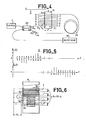
- FIG. 4 represents a particular embodiment of the coherent signal processing device according to the invention. Like the previous one, it includes a source 1, a bidirectional coupler 20, a coil of single-mode optical fiber 25 at one end of which are placed in series on the optical fiber of the basic modulators, and at the other end of which is placed the modulator M G . However, in this embodiment, the modulators are all produced on the same circuit M.
- G n , n 11 in the figure, provided with control electrodes arranged in a conventional manner on either side of the guide, and not shown in the figure, for the introduction of a phase shift due to the electric field applied to the guides.
- Pieces of optical fiber of length adapted to the delay ⁇ to be introduced between two modulators connect the output of one guide to the input of the next, for example according to the configuration shown in FIG. 4, where the output of a modulator and the input of the next modulator are produced on the same side face of the integrated optical circuit.
- This arrangement is not limiting and all the inputs of the modulators can be arranged on the same lateral face of the integrated optical circuit and all the outputs on the other face, optical fiber loops being adapted accordingly.
- the access to the directional coupler located on the same side as the source is connected to a detector 30.
- the electrical signal applied to the control input E C is an electrical pulse which introduces a phase modulation of the optical wave simultaneously on the light wave propagating on the optical figure, and therefore at times spaced from ⁇ on l continuous optical wave transmitted by the source.
- the length of the electrodes of each of the elementary modulators, whether they are produced independently or produced on the same integrated optical circuit determines the phase shift applied, and the direction of this phase shift is fixed by the direction of the electric field applied to these electrodes. By a particular configuration of the electrodes it is therefore possible to obtain phase shifts ⁇ 1 (t) and ⁇ 2 (t) on the two counter-rotating ⁇ 1 and ⁇ 2 waves in the fiber loop 25. An example of these phase shifts is shown in FIG.
- the wave ⁇ 1 first undergoes modulation by the modulator produced from the guide G1 while the counter-rotating wave ⁇ 2 first undergoes a phase shift by the modulator produced from the guide G11.
- FIG. 6 partially represents an embodiment of the modulator M where the control electrodes of the phase modulators have been represented, assuming that the phase shifts applied are those represented in FIG. 5.
- Each guide G1, G2, G3, G4 is associated with suitably configured control electrodes. These control electrodes are interconnected. In the example shown, the control voltage has the same direction for the first four modulators.
- the invention is not limited to the embodiments described and shown.
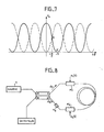
- the linear part of the sinusoidal response of the interferometer shown in FIG. 7 is used to detect phase differences.
- the interferometer is placed "at an angle" in the linear zone, that is to say that a phase modulator, M G , placed at one end of the fiber creates an additional phase modulation alternately of + and - , at the rate of the fiber travel time and therefore a additional phase shift equal to which places the operating point of the interferometer at point G of the sinusoidal response, FIG. 7, the phase variations resulting in power variations around this point.
- the non-linear part of the sinusoidal response of the interferometer can detect signals whose processing has been carried out at high frequency, for example around 10 GHz, in a lower frequency band, 10 to 100 MHz for example.
- This processing using the quadratic part of the response of the interferometer as a function of the phase applies for example to the performance of functions such as inter-correlation, auto-correlation or spectrum analysis.
- FIG. 8 illustrates an embodiment of the processing device according to the invention: a source 1 is connected to the first access A of a 3dB coupler, 20, which distributes the incident optical wave between the two ends of a loop of optical fiber 25, themselves coupled to the ports C and D of the coupler 20.
- Two phase modulators M ⁇ 1 and M ⁇ 2 controlled by electrical signals respectively s1 (t) and s2 (t) create phase modulations respectively ⁇ 1 (t) and ⁇ 2 (t).
- the phase difference between the two counter-rotating waves is ⁇ , that is to say that the operating point on the characteristic of FIG. 7 is G ⁇
- the intensity of the light on the detector 30 coupled to the fourth port, B, of the coupler 20 is a function of the product ⁇ 1 (t) . ⁇ 2 (t).
- the detected intensity is a function of ⁇ 1 (t) ⁇ 2 (t) dt where td is the detector response time.
- the optical fiber 25 between M ⁇ 1 and M ⁇ 2 can be a fiber with high dispersion so that the information applied via s1 (t) on the wave traversing the fiber in the direction "-" is filtered, and likewise for the information applied via s2 (t) on the wave traversing the fiber in the direction "+".
- the optical wave can be amplified by any known means.
- This amplification, in the loop, or even downstream, can for example be carried out by stimulated "RAMAN” effect (by transfer of energy from a pump signal to the optical wave), by optical semiconductor amplification, or by coupling of waves.
- s1 (t) s (t)
- signal to be analyzed s2 (t) cos ⁇ t (or sin ⁇ t)
- ⁇ 2 ⁇ (f + f ⁇ t)
- This signal is therefore directly linked to the Fourier transform of s (t): s (t) cos ( ⁇ t) dt It is possible to obtain the real part or the imaginary part of the Fourier transform using two similar circuits.
- the structure represented in FIG. 3 with several modulators controlled by the same signal, ie s (t), can be associated with the structure represented in FIG. 8 for allow the signal to be repeated, at a rate equal to the propagation time between modulators, a number of times equal to the number of modulators:
- the modulator M G shown in FIGS. 3, 4 and 8 can in practice be integrated with the bidirectional coupler 20, the device thus using a multifunction integrated optical circuit.
Landscapes
- Physics & Mathematics (AREA)
- Nonlinear Science (AREA)
- Engineering & Computer Science (AREA)
- Theoretical Computer Science (AREA)
- Mathematical Physics (AREA)
- Optics & Photonics (AREA)
- General Physics & Mathematics (AREA)
- Optical Communication System (AREA)
- Optical Integrated Circuits (AREA)
Applications Claiming Priority (2)
| Application Number | Priority Date | Filing Date | Title |
|---|---|---|---|
| FR8704725A FR2613564B1 (fr) | 1987-04-03 | 1987-04-03 | Dispositif de traitement de signal coherent utilisant une ligne a retard optique |
| FR8704725 | 1987-04-03 |
Publications (1)
| Publication Number | Publication Date |
|---|---|
| EP0285523A1 true EP0285523A1 (de) | 1988-10-05 |
Family
ID=9349775
Family Applications (1)
| Application Number | Title | Priority Date | Filing Date |
|---|---|---|---|
| EP88400803A Withdrawn EP0285523A1 (de) | 1987-04-03 | 1988-04-01 | Kohärentsignalverarbeitungsvorrichtung mit einer optischen Verzögerungsleitung und ihre Verwendung als Filter, Korrelator und Spektrumanalysator |
Country Status (3)
| Country | Link |
|---|---|
| EP (1) | EP0285523A1 (de) |
| JP (1) | JPS63265217A (de) |
| FR (1) | FR2613564B1 (de) |
Cited By (1)
| Publication number | Priority date | Publication date | Assignee | Title |
|---|---|---|---|---|
| FR2642923A1 (en) * | 1989-02-03 | 1990-08-10 | Thomson Csf | Device for optical signal processing, especially for microwave signals, with evanescent-wave optical couplers, and use of such a device |
Families Citing this family (1)
| Publication number | Priority date | Publication date | Assignee | Title |
|---|---|---|---|---|
| JP4983149B2 (ja) * | 2006-08-21 | 2012-07-25 | 富士通株式会社 | 光送信器 |
Family Cites Families (1)
| Publication number | Priority date | Publication date | Assignee | Title |
|---|---|---|---|---|
| JPS59195220A (ja) * | 1983-04-20 | 1984-11-06 | Masayuki Izutsu | 光学的検出装置 |
-
1987
- 1987-04-03 FR FR8704725A patent/FR2613564B1/fr not_active Expired
-
1988
- 1988-04-01 EP EP88400803A patent/EP0285523A1/de not_active Withdrawn
- 1988-04-04 JP JP63082841A patent/JPS63265217A/ja active Pending
Non-Patent Citations (3)
| Title |
|---|
| IEEE TRANSACTIONS ON MICROWAVE THEORY AND TECHNIQUES, vol. MTT-33, no. 3, mars 1985, pages 193-210, IEEE; K.P. JACKSON et al.: "Optical fiber delay-line signal processing" * |
| JOURNAL OF LIGHTWAVE TECHNOLOGY, vol. LT-4, no. 7, juillet 1986, pages 852-857, IEEE, New York, US; W.A. STALLARD et al.: "Integrated optic devices for coherent transmission" * |
| PATENT ABSTRACTS OF JAPAN, vol. 9, no. 58 (P-341)[1781], 14 mars 1985; & JP-A-59 195 220 (MASAYUKI IZUTSU) 06-11-1984 * |
Cited By (1)
| Publication number | Priority date | Publication date | Assignee | Title |
|---|---|---|---|---|
| FR2642923A1 (en) * | 1989-02-03 | 1990-08-10 | Thomson Csf | Device for optical signal processing, especially for microwave signals, with evanescent-wave optical couplers, and use of such a device |
Also Published As
| Publication number | Publication date |
|---|---|
| JPS63265217A (ja) | 1988-11-01 |
| FR2613564B1 (fr) | 1989-06-23 |
| FR2613564A1 (fr) | 1988-10-07 |
Similar Documents
| Publication | Publication Date | Title |
|---|---|---|
| EP0020216B1 (de) | Numerisch gesteuerter optischer Intensitätsmodulator in integrierter optischer Form und Digital-Analog-Umsetzer mit einem solchen Modulator | |
| EP0068949B1 (de) | Verfahren zur optischen Analog-/Digitalumwandlung und entsprechender Wandler | |
| EP0531499B1 (de) | Optisch arbeitender elektrischer transversaler filter | |
| EP0603036B1 (de) | Optische Verarbeitungsvorrichtung für elektrische Signale | |
| EP0017571B1 (de) | Lichtintensitätsmodulator in integrierter Optik und integrierte optische Schaltung mit einem solchen Modulator | |
| EP0835559B1 (de) | Verfahren und vorrichtung zur schätzung von nichtlinearität | |
| EP0853395A1 (de) | Vorrichtung zur Polarisationsdispersionskompensation in einem optischen Übertragungssystem | |
| EP0266249B1 (de) | Dreiachsiges optisches Fiberringinterferometer | |
| CA1108431A (fr) | Echometre pour la localisation de defauts affectant les conducteurs de lumiere | |
| US5376786A (en) | Optoelectronic transversal filter with variable gain bi-polar taps | |
| EP0099282B1 (de) | Von der Polarisation unabhängiger integriert-optischer Modulator | |
| EP0048640B1 (de) | Einrichtung zum Trennen zweier Lichtsignale, welche von Quellen verschiedener Wellenlänge ausgestrahlt und auf eine selbe optische Faser übertragen werden, und Empfänger, welcher eine derartige Einrichtung enthält | |
| EP0816896A2 (de) | Optisches Bauelement | |
| EP0285523A1 (de) | Kohärentsignalverarbeitungsvorrichtung mit einer optischen Verzögerungsleitung und ihre Verwendung als Filter, Korrelator und Spektrumanalysator | |
| EP1782027B1 (de) | Impulsprofil-messeinrichtung | |
| FR2662805A1 (fr) | Capteur de rotation optique a fibre. | |
| EP0094866B1 (de) | Gerät für busartige wechselseitige Verbindung mit monomoden Lichtwellenleitern | |
| FR2640379A1 (fr) | Procede d'analyse de composants d'optique guidee, fibres optiques ou reseaux de guides optiques par reflectometrie temporelle et reflectometre dans le domaine temporel | |
| JP2002023211A (ja) | 光信号のタイミングを制御する時間補償アーキテクチャ | |
| FR2797331A1 (fr) | Differenciateur optique | |
| EP1158352A2 (de) | Optischer NRZ-RZ-Wandler | |
| US5136532A (en) | Coherent signal processing device using an optical delay line and application thereof to filtering correlation product and spectral analysis | |
| EP0421880B1 (de) | Polyvalentes integriertes optisches Bauteil und Verteilungsnetz mit optischer Verstärkung | |
| FR2660441A1 (fr) | Coupleur bidirectionnel en optique integree monomode. | |
| FR2680060A1 (fr) | Procede de transmission par fibre optique d'un signal, issu d'un capteur, notamment d'un hydrophone. |
Legal Events
| Date | Code | Title | Description |
|---|---|---|---|
| PUAI | Public reference made under article 153(3) epc to a published international application that has entered the european phase |
Free format text: ORIGINAL CODE: 0009012 |
|
| AK | Designated contracting states |
Kind code of ref document: A1 Designated state(s): DE FR GB IT NL SE |
|
| 17P | Request for examination filed |
Effective date: 19890320 |
|
| RAP3 | Party data changed (applicant data changed or rights of an application transferred) |
Owner name: THOMSON-CSF |
|
| 17Q | First examination report despatched |
Effective date: 19910716 |
|
| RAP1 | Party data changed (applicant data changed or rights of an application transferred) |
Owner name: THOMSON-CSF |
|
| STAA | Information on the status of an ep patent application or granted ep patent |
Free format text: STATUS: THE APPLICATION IS DEEMED TO BE WITHDRAWN |
|
| 18D | Application deemed to be withdrawn |
Effective date: 19931103 |