EP0286410B1 - Verfahren zur Herstellung keramischer Supraleiter - Google Patents
Verfahren zur Herstellung keramischer Supraleiter Download PDFInfo
- Publication number
- EP0286410B1 EP0286410B1 EP88303124A EP88303124A EP0286410B1 EP 0286410 B1 EP0286410 B1 EP 0286410B1 EP 88303124 A EP88303124 A EP 88303124A EP 88303124 A EP88303124 A EP 88303124A EP 0286410 B1 EP0286410 B1 EP 0286410B1
- Authority
- EP
- European Patent Office
- Prior art keywords
- layer
- superconducting
- ceramic
- coil
- laser beam
- Prior art date
- Legal status (The legal status is an assumption and is not a legal conclusion. Google has not performed a legal analysis and makes no representation as to the accuracy of the status listed.)
- Expired - Lifetime
Links
- 238000000034 method Methods 0.000 title claims description 21
- 239000002887 superconductor Substances 0.000 title claims description 9
- 229910010293 ceramic material Inorganic materials 0.000 title claims description 8
- 238000004519 manufacturing process Methods 0.000 title claims description 8
- 239000000919 ceramic Substances 0.000 claims description 37
- 239000000758 substrate Substances 0.000 claims description 19
- MCMNRKCIXSYSNV-UHFFFAOYSA-N Zirconium dioxide Chemical compound O=[Zr]=O MCMNRKCIXSYSNV-UHFFFAOYSA-N 0.000 claims description 6
- 239000000463 material Substances 0.000 claims description 6
- 238000004544 sputter deposition Methods 0.000 claims description 5
- RUDFQVOCFDJEEF-UHFFFAOYSA-N yttrium(III) oxide Inorganic materials [O-2].[O-2].[O-2].[Y+3].[Y+3] RUDFQVOCFDJEEF-UHFFFAOYSA-N 0.000 claims description 5
- 238000000137 annealing Methods 0.000 claims description 2
- VEALVRVVWBQVSL-UHFFFAOYSA-N strontium titanate Chemical compound [Sr+2].[O-][Ti]([O-])=O VEALVRVVWBQVSL-UHFFFAOYSA-N 0.000 claims description 2
- 229910052845 zircon Inorganic materials 0.000 claims description 2
- GFQYVLUOOAAOGM-UHFFFAOYSA-N zirconium(iv) silicate Chemical compound [Zr+4].[O-][Si]([O-])([O-])[O-] GFQYVLUOOAAOGM-UHFFFAOYSA-N 0.000 claims description 2
- 230000001678 irradiating effect Effects 0.000 claims 4
- 238000000151 deposition Methods 0.000 claims 2
- 230000008021 deposition Effects 0.000 claims 1
- 239000010408 film Substances 0.000 description 25
- 230000000737 periodic effect Effects 0.000 description 13
- 238000000859 sublimation Methods 0.000 description 7
- 230000008022 sublimation Effects 0.000 description 7
- 239000007769 metal material Substances 0.000 description 4
- 239000010409 thin film Substances 0.000 description 4
- 239000010949 copper Substances 0.000 description 3
- 238000010304 firing Methods 0.000 description 3
- 238000005224 laser annealing Methods 0.000 description 3
- RYGMFSIKBFXOCR-UHFFFAOYSA-N Copper Chemical compound [Cu] RYGMFSIKBFXOCR-UHFFFAOYSA-N 0.000 description 2
- FYYHWMGAXLPEAU-UHFFFAOYSA-N Magnesium Chemical compound [Mg] FYYHWMGAXLPEAU-UHFFFAOYSA-N 0.000 description 2
- 229910052784 alkaline earth metal Inorganic materials 0.000 description 2
- 150000001342 alkaline earth metals Chemical class 0.000 description 2
- QVGXLLKOCUKJST-UHFFFAOYSA-N atomic oxygen Chemical group [O] QVGXLLKOCUKJST-UHFFFAOYSA-N 0.000 description 2
- 229910052790 beryllium Inorganic materials 0.000 description 2
- ATBAMAFKBVZNFJ-UHFFFAOYSA-N beryllium atom Chemical compound [Be] ATBAMAFKBVZNFJ-UHFFFAOYSA-N 0.000 description 2
- 230000000694 effects Effects 0.000 description 2
- 229910052749 magnesium Inorganic materials 0.000 description 2
- 239000011777 magnesium Substances 0.000 description 2
- 230000003647 oxidation Effects 0.000 description 2
- 238000007254 oxidation reaction Methods 0.000 description 2
- 239000001301 oxygen Substances 0.000 description 2
- 229910052760 oxygen Inorganic materials 0.000 description 2
- 229910001233 yttria-stabilized zirconia Inorganic materials 0.000 description 2
- 229910017083 AlN Inorganic materials 0.000 description 1
- PIGFYZPCRLYGLF-UHFFFAOYSA-N Aluminum nitride Chemical compound [Al]#N PIGFYZPCRLYGLF-UHFFFAOYSA-N 0.000 description 1
- BVKZGUZCCUSVTD-UHFFFAOYSA-L Carbonate Chemical compound [O-]C([O-])=O BVKZGUZCCUSVTD-UHFFFAOYSA-L 0.000 description 1
- 241000272194 Ciconiiformes Species 0.000 description 1
- 229910000881 Cu alloy Inorganic materials 0.000 description 1
- 229910000750 Niobium-germanium Inorganic materials 0.000 description 1
- 229910052581 Si3N4 Inorganic materials 0.000 description 1
- VYPSYNLAJGMNEJ-UHFFFAOYSA-N Silicium dioxide Chemical compound O=[Si]=O VYPSYNLAJGMNEJ-UHFFFAOYSA-N 0.000 description 1
- PNEYBMLMFCGWSK-UHFFFAOYSA-N aluminium oxide Inorganic materials [O-2].[O-2].[O-2].[Al+3].[Al+3] PNEYBMLMFCGWSK-UHFFFAOYSA-N 0.000 description 1
- 229910052787 antimony Inorganic materials 0.000 description 1
- 229910052785 arsenic Inorganic materials 0.000 description 1
- 229910052797 bismuth Inorganic materials 0.000 description 1
- 229910052796 boron Inorganic materials 0.000 description 1
- 238000003486 chemical etching Methods 0.000 description 1
- 229910052802 copper Inorganic materials 0.000 description 1
- 230000007547 defect Effects 0.000 description 1
- 230000001419 dependent effect Effects 0.000 description 1
- 239000011521 glass Substances 0.000 description 1
- 229910052736 halogen Inorganic materials 0.000 description 1
- 150000002367 halogens Chemical class 0.000 description 1
- 239000001307 helium Substances 0.000 description 1
- 229910052734 helium Inorganic materials 0.000 description 1
- SWQJXJOGLNCZEY-UHFFFAOYSA-N helium atom Chemical compound [He] SWQJXJOGLNCZEY-UHFFFAOYSA-N 0.000 description 1
- 239000007788 liquid Substances 0.000 description 1
- 229910052751 metal Inorganic materials 0.000 description 1
- 239000002184 metal Substances 0.000 description 1
- 239000000203 mixture Substances 0.000 description 1
- 230000003287 optical effect Effects 0.000 description 1
- 238000000059 patterning Methods 0.000 description 1
- 229910052761 rare earth metal Inorganic materials 0.000 description 1
- 238000001953 recrystallisation Methods 0.000 description 1
- HQVNEWCFYHHQES-UHFFFAOYSA-N silicon nitride Chemical compound N12[Si]34N5[Si]62N3[Si]51N64 HQVNEWCFYHHQES-UHFFFAOYSA-N 0.000 description 1
- 229910052814 silicon oxide Inorganic materials 0.000 description 1
- 239000006104 solid solution Substances 0.000 description 1
- 238000005092 sublimation method Methods 0.000 description 1
Images
Classifications
-
- H—ELECTRICITY
- H10—SEMICONDUCTOR DEVICES; ELECTRIC SOLID-STATE DEVICES NOT OTHERWISE PROVIDED FOR
- H10N—ELECTRIC SOLID-STATE DEVICES NOT OTHERWISE PROVIDED FOR
- H10N60/00—Superconducting devices
- H10N60/01—Manufacture or treatment
- H10N60/0268—Manufacture or treatment of devices comprising copper oxide
- H10N60/0661—Processes performed after copper oxide formation, e.g. patterning
-
- H—ELECTRICITY
- H10—SEMICONDUCTOR DEVICES; ELECTRIC SOLID-STATE DEVICES NOT OTHERWISE PROVIDED FOR
- H10N—ELECTRIC SOLID-STATE DEVICES NOT OTHERWISE PROVIDED FOR
- H10N60/00—Superconducting devices
- H10N60/01—Manufacture or treatment
- H10N60/0268—Manufacture or treatment of devices comprising copper oxide
- H10N60/0296—Processes for depositing or forming copper oxide superconductor layers
- H10N60/0576—Processes for depositing or forming copper oxide superconductor layers characterised by the substrate
-
- H—ELECTRICITY
- H01—ELECTRIC ELEMENTS
- H01F—MAGNETS; INDUCTANCES; TRANSFORMERS; SELECTION OF MATERIALS FOR THEIR MAGNETIC PROPERTIES
- H01F41/00—Apparatus or processes specially adapted for manufacturing or assembling magnets, inductances or transformers; Apparatus or processes specially adapted for manufacturing materials characterised by their magnetic properties
- H01F41/02—Apparatus or processes specially adapted for manufacturing or assembling magnets, inductances or transformers; Apparatus or processes specially adapted for manufacturing materials characterised by their magnetic properties for manufacturing cores, coils, or magnets
- H01F41/04—Apparatus or processes specially adapted for manufacturing or assembling magnets, inductances or transformers; Apparatus or processes specially adapted for manufacturing materials characterised by their magnetic properties for manufacturing cores, coils, or magnets for manufacturing coils
- H01F41/048—Superconductive coils
-
- H—ELECTRICITY
- H01—ELECTRIC ELEMENTS
- H01F—MAGNETS; INDUCTANCES; TRANSFORMERS; SELECTION OF MATERIALS FOR THEIR MAGNETIC PROPERTIES
- H01F6/00—Superconducting magnets; Superconducting coils
- H01F6/06—Coils, e.g. winding, insulating, terminating or casing arrangements therefor
-
- H—ELECTRICITY
- H10—SEMICONDUCTOR DEVICES; ELECTRIC SOLID-STATE DEVICES NOT OTHERWISE PROVIDED FOR
- H10N—ELECTRIC SOLID-STATE DEVICES NOT OTHERWISE PROVIDED FOR
- H10N60/00—Superconducting devices
- H10N60/01—Manufacture or treatment
- H10N60/0268—Manufacture or treatment of devices comprising copper oxide
- H10N60/0296—Processes for depositing or forming copper oxide superconductor layers
- H10N60/0408—Processes for depositing or forming copper oxide superconductor layers by sputtering
-
- H—ELECTRICITY
- H10—SEMICONDUCTOR DEVICES; ELECTRIC SOLID-STATE DEVICES NOT OTHERWISE PROVIDED FOR
- H10N—ELECTRIC SOLID-STATE DEVICES NOT OTHERWISE PROVIDED FOR
- H10N60/00—Superconducting devices
- H10N60/01—Manufacture or treatment
- H10N60/0268—Manufacture or treatment of devices comprising copper oxide
- H10N60/0296—Processes for depositing or forming copper oxide superconductor layers
- H10N60/0521—Processes for depositing or forming copper oxide superconductor layers by pulsed laser deposition, e.g. laser sputtering
-
- Y—GENERAL TAGGING OF NEW TECHNOLOGICAL DEVELOPMENTS; GENERAL TAGGING OF CROSS-SECTIONAL TECHNOLOGIES SPANNING OVER SEVERAL SECTIONS OF THE IPC; TECHNICAL SUBJECTS COVERED BY FORMER USPC CROSS-REFERENCE ART COLLECTIONS [XRACs] AND DIGESTS
- Y10—TECHNICAL SUBJECTS COVERED BY FORMER USPC
- Y10S—TECHNICAL SUBJECTS COVERED BY FORMER USPC CROSS-REFERENCE ART COLLECTIONS [XRACs] AND DIGESTS
- Y10S428/00—Stock material or miscellaneous articles
- Y10S428/922—Static electricity metal bleed-off metallic stock
- Y10S428/9265—Special properties
- Y10S428/93—Electric superconducting
-
- Y—GENERAL TAGGING OF NEW TECHNOLOGICAL DEVELOPMENTS; GENERAL TAGGING OF CROSS-SECTIONAL TECHNOLOGIES SPANNING OVER SEVERAL SECTIONS OF THE IPC; TECHNICAL SUBJECTS COVERED BY FORMER USPC CROSS-REFERENCE ART COLLECTIONS [XRACs] AND DIGESTS
- Y10—TECHNICAL SUBJECTS COVERED BY FORMER USPC
- Y10S—TECHNICAL SUBJECTS COVERED BY FORMER USPC CROSS-REFERENCE ART COLLECTIONS [XRACs] AND DIGESTS
- Y10S505/00—Superconductor technology: apparatus, material, process
- Y10S505/70—High TC, above 30 k, superconducting device, article, or structured stock
- Y10S505/701—Coated or thin film device, i.e. active or passive
- Y10S505/703—Microelectronic device with superconducting conduction line
-
- Y—GENERAL TAGGING OF NEW TECHNOLOGICAL DEVELOPMENTS; GENERAL TAGGING OF CROSS-SECTIONAL TECHNOLOGIES SPANNING OVER SEVERAL SECTIONS OF THE IPC; TECHNICAL SUBJECTS COVERED BY FORMER USPC CROSS-REFERENCE ART COLLECTIONS [XRACs] AND DIGESTS
- Y10—TECHNICAL SUBJECTS COVERED BY FORMER USPC
- Y10S—TECHNICAL SUBJECTS COVERED BY FORMER USPC CROSS-REFERENCE ART COLLECTIONS [XRACs] AND DIGESTS
- Y10S505/00—Superconductor technology: apparatus, material, process
- Y10S505/70—High TC, above 30 k, superconducting device, article, or structured stock
- Y10S505/704—Wire, fiber, or cable
- Y10S505/705—Magnetic coil
-
- Y—GENERAL TAGGING OF NEW TECHNOLOGICAL DEVELOPMENTS; GENERAL TAGGING OF CROSS-SECTIONAL TECHNOLOGIES SPANNING OVER SEVERAL SECTIONS OF THE IPC; TECHNICAL SUBJECTS COVERED BY FORMER USPC CROSS-REFERENCE ART COLLECTIONS [XRACs] AND DIGESTS
- Y10—TECHNICAL SUBJECTS COVERED BY FORMER USPC
- Y10S—TECHNICAL SUBJECTS COVERED BY FORMER USPC CROSS-REFERENCE ART COLLECTIONS [XRACs] AND DIGESTS
- Y10S505/00—Superconductor technology: apparatus, material, process
- Y10S505/725—Process of making or treating high tc, above 30 k, superconducting shaped material, article, or device
- Y10S505/728—Etching
-
- Y—GENERAL TAGGING OF NEW TECHNOLOGICAL DEVELOPMENTS; GENERAL TAGGING OF CROSS-SECTIONAL TECHNOLOGIES SPANNING OVER SEVERAL SECTIONS OF THE IPC; TECHNICAL SUBJECTS COVERED BY FORMER USPC CROSS-REFERENCE ART COLLECTIONS [XRACs] AND DIGESTS
- Y10—TECHNICAL SUBJECTS COVERED BY FORMER USPC
- Y10S—TECHNICAL SUBJECTS COVERED BY FORMER USPC CROSS-REFERENCE ART COLLECTIONS [XRACs] AND DIGESTS
- Y10S505/00—Superconductor technology: apparatus, material, process
- Y10S505/725—Process of making or treating high tc, above 30 k, superconducting shaped material, article, or device
- Y10S505/73—Vacuum treating or coating
- Y10S505/731—Sputter coating
-
- Y—GENERAL TAGGING OF NEW TECHNOLOGICAL DEVELOPMENTS; GENERAL TAGGING OF CROSS-SECTIONAL TECHNOLOGIES SPANNING OVER SEVERAL SECTIONS OF THE IPC; TECHNICAL SUBJECTS COVERED BY FORMER USPC CROSS-REFERENCE ART COLLECTIONS [XRACs] AND DIGESTS
- Y10—TECHNICAL SUBJECTS COVERED BY FORMER USPC
- Y10S—TECHNICAL SUBJECTS COVERED BY FORMER USPC CROSS-REFERENCE ART COLLECTIONS [XRACs] AND DIGESTS
- Y10S505/00—Superconductor technology: apparatus, material, process
- Y10S505/725—Process of making or treating high tc, above 30 k, superconducting shaped material, article, or device
- Y10S505/742—Annealing
-
- Y—GENERAL TAGGING OF NEW TECHNOLOGICAL DEVELOPMENTS; GENERAL TAGGING OF CROSS-SECTIONAL TECHNOLOGIES SPANNING OVER SEVERAL SECTIONS OF THE IPC; TECHNICAL SUBJECTS COVERED BY FORMER USPC CROSS-REFERENCE ART COLLECTIONS [XRACs] AND DIGESTS
- Y10—TECHNICAL SUBJECTS COVERED BY FORMER USPC
- Y10T—TECHNICAL SUBJECTS COVERED BY FORMER US CLASSIFICATION
- Y10T428/00—Stock material or miscellaneous articles
- Y10T428/24—Structurally defined web or sheet [e.g., overall dimension, etc.]
- Y10T428/24802—Discontinuous or differential coating, impregnation or bond [e.g., artwork, printing, retouched photograph, etc.]
- Y10T428/24926—Discontinuous or differential coating, impregnation or bond [e.g., artwork, printing, retouched photograph, etc.] including ceramic, glass, porcelain or quartz layer
Definitions
- This invention relates to methods of manufacturing ceramic material superconductors by light irradiation.
- the present invention resides generally in the concept of providing a layer of a prescribed material on a substrate, treating the said layer by for example thermal oxidation or firing to convert it into a superconducting layer and scribing a pattern into the layer by irradiation in order to obtain a superconducting ceramic with desired characteristics. It is unimportant to the working of the invention whether the pattern is scribed into the layer before or after it is converted into a superconducting layer since the invention takes advantage of the fact that the material forming the layer will undergo sublimation when irradiated by a suitable source and proposes to provide hitherto unobtainable high Tc superconducting structures.
- an oxide (or carbonate) mixture for constituting a superconducting ceramic is first deposited in the form of a thin film onto a substrate by sputtering, printing such as screen press printing or other methods.
- sputtering printing such as screen press printing or other methods.
- the resultant film adopts an amorphous or other structure which gives rise to abundant lattice defects and/or imperfections so that the resistivity of the ceramic material is usually rather high.
- the deposited ceramic film can be transformed into a desired superconducting ceramic by thermal oxidation or firing.
- the ceramic film can be processed by laser irradiation before or after firing and can be arranged such that for example a strip of the ceramic material is removed from or remains on the substrate.
- Any suitable laser can be used to irradiate the layer in order to scribe the desired pattern into the layer and may for example be a YAG laser emitting a circular beam of light with a wavelength of about 1.06 microns pulsed at between 5 and 100 KHz, an excimer laser (KrF, KrCl and so forth), a C02 laser or an N2 laser.
- a shaped beam having a circular cross-section with a diameter from 10 to 100 microns is emitted and a beam with a linear cross section typically from 10 to 40 cm wide and from 5 to 100 microns long can be obtained therefrom by expanding and squeezing the circular beam with an optical system.
- Groups Ia, IIa, VIII, Ib, IIb and 0 are the same in the Japanese and European Periodic Tables
- Groups IIIa, IVa, Va, VIa and VIIa of the Japanese Periodic Table correspond respectively to Groups IIIb, IVb, Vb, VIb and VIIb of the European Periodic Table
- Groups IIIb, IVb, Vb, VIb and VIIb of the Japanese Periodic Table correspond respectively to Groups IIIa,, IVa, Va, VIa and VIIa of the European Periodic Table.
- a substrate 1 may be made of a ceramic material such as alumina, silicon oxide, silicon nitride, aluminium nitride, strontium titanate, zirconia, yttria or YSZ(yttria stabilized zircon), or a metal such as copper or a copper alloy or glass.
- YSZ, yttria or zirconia are particularly suitable having regard to the desirability of matching the coefficient of thermal expansion to that of the layer formed thereon as hereinafter described.
- the material should be selected so that the differential coefficient of thermal expansion between the underlying substrate and the overlying ceramic thin film should be limited preferably within 50% of the thermal expansion coefficient of the ceramic thin film, since if the thermal expansion coefficients of the substrate and the ceramic thin film are substantially different, then the strain developed between them may hinder the recrystallisation of the ceramic film into a superconducting structure during thermal annealing.
- the next step is to fire the same at a temperature from 500 to 1000°C e.g. 900°C for 15 hours whereby the ceramic film 2 is transformed into a superconducting structure.
- a laser beam 1.06 microns in wavelength derived by means of a YAG laser may be used to irradiate parts of the superconducting film 2 in order to produce a pattern thereon.
- the surface of the film has been scanned from the left edge towards the middle of the structure so as to remove a portion of the film by sublimation and thereby leave a groove 3.
- the output power of the laser should be from 106 to 107 W/sec; stronger irradiation may damage the underlying substrate 1.
- the laser patterning can be effected before the structure is fired to transform the ceramic film into a superconducting layer in which oxygen and copper atoms form the structure of the layer.
- Each circular pulse emitted from the laser is directed towards a predefined irradiation region on the film which region is common to 60 to 80% of the irradiation region of the preceding pulse (and also of the subsequent pulse).
- the scanning speed is typically 2m/min.
- the frequency can be from 5 to 30 KHz, e.g. 10 KHz.
- an excimer laser which is capable of emitting a series of intense laser pulses with a rectangular cross section of for example 20 x 30 mm2 can be used in which case, the emitted pulse can be shaped into a linear cross-section 10 cm wide and 50 microns thick.
- the effect of this irradiation is to selectively remove the irradiated portions of the ceramic film by sublimation.
- the entire structure can be heated during this laser scribing process to a temperature from 300 to 800°C, e.g. 600°C by a halogen lamp in order to enhance sublimation.
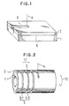
- Fig.2 shows a second embodiment of the invention.
- the substrate 1 is a cylinder and a ceramic film 2 is deposited on the substrate 1 while the substrate 1 is rotating the direction indicated by an arrow 12.
- a laser beam 50 microns in diameter, is radiated continuously or repeatedly towards the substrate.
- the laser beam is shifted towards the right as seen in the drawing (the axial direction of the cylinder 1) while the substrate 1 is rotated around its axis.
- a helical groove 3 is scribed into the layer 2 thereby forming a continuous helical superconductor 5 on the cylinder 1.
- each part of the helix 5-1 is isolated from adjacent parts 5-2 by the helical groove 3 which has been removed by the above described laser sublimation scribing process and thus a superconducting electromagnet in the form of a coil is constructed.
- a superconductor of superior quality can be obtained.
- a ceramic film is initially formed on the surface of a substrate by for example sputtering.
- the film initially has an amorphous or other non-superconducting structure.
- laser annealing a prescribed portion of the film is melted by irradiation with a laser beam which portion recrystallises into a superconducting atomic structure when cooled. If necessary the whole structure, i.e. the substrate and the ceramic film, may be cooled at the same time.
- Superconducting ceramics in accordance with the present invention also may be prepared in accordance with the stoichiometric formulae (A 1-x B x ) y Cu z 0 w , where A is one or more elements of Group IIIa of the Japanese Periodic Table, e.g., the rare earth elements, B is one or more elements of Group IIa of the Japanese Periodic Table, e.g.
- YBa2Cu306 ⁇ 8 is YBa2Cu306 ⁇ 8.
- superconducting ceramics in accordance with the present invention may be prepared in accordance with the stoichiometric formulae (A1 ⁇ x B x ) y Cu z 0 w , where A is one or more elements of Group Vb of the Periodic Table such as Bi, Sb and As, B is one or more elements of Group IIa of the Periodic Table, e.g.
- Examples of this general formula are BiSrCaCuCu20 x and Bi4Sr3Ca3Cu40 x .
- Tc onset and Tco samples confirmed consistent with the formula Bi4Sr y Ca3Cu40 x (y is around 1.5) were measured to be 40-60°K, which is not notably high, but relatively high critical temperatures were obtained with samples conforming to the stoichiometric formulae Bi4Sr4Ca2Cu40 x and Bi2Sr3Ca2Cu20 x .
- the number designating the oxygen proportion is in the range 6 to 10, e.g. around 8.1.
Landscapes
- Engineering & Computer Science (AREA)
- Power Engineering (AREA)
- Manufacturing & Machinery (AREA)
- Physics & Mathematics (AREA)
- Optics & Photonics (AREA)
- Superconductors And Manufacturing Methods Therefor (AREA)
- Superconductor Devices And Manufacturing Methods Thereof (AREA)
- Compositions Of Oxide Ceramics (AREA)
- Inorganic Compounds Of Heavy Metals (AREA)
- Physical Vapour Deposition (AREA)
Claims (11)
- Verfahren zum Herstellen eines keramischen Supraleiters, umfassend:- Ausbilden einer Keramikschicht aus supraleitendem Material auf einer Oberfläche aus einem Material, das einen thermischen Expansionskoeffizienten aufweist, der 50 % bis 150 % desjenigen der Keramikschicht beträgt; und- Bestrahlen eines Teils der Keramikschicht in solcher Weise, daß bewirkt wird, daß der bestrahlte Teil der Keramikschicht von der Oberfläche entfernt wird.
- Verfahren nach Anspruch 1, bei dem der Herstellschritt für die supraleitende Keramikschicht das Belegen der Oberfläche durch Sputtern umfaßt.
- Verfahren nach einem der vorstehenden Ansprüche, bei dem das Substrat aus Strontiumtitanat, Zirkoniumdioxid, Yttriumoxid oder YSZ (mit Yttriumoxid stabilisiertes Zirkonium) besteht.
- Verfahren nach einem der vorstehenden Ansprüche, bei dem der Laserstrahl in einer Impulsfolge auf die Schicht angewandt wird.
- Verfahren nach Anspruch 4, bei dem die Impulse so auf einen Teil der Keramikschicht gestrahlt werden, daß einer vorgegebenen Linie auf derselben gefolgt wird.
- Verfahren nach einem der vorstehenden Ansprüche, bei dem der Laserstrahl so auf die Schicht gestrahlt wird, daß eine supraleitende Spule gebildet wird.
- Verfahren nach Anspruch 6, bei dem die genannte Fläche der Umfang eines Zylinders ist, der während des Bestrahlungsschritts um seine Achse gedreht wird, und daß der Ort des Laserstrahls auf der Schicht in axialer Richtung des Zylinders verschoben wird, wodurch der Laserstrahl einem schraubenförmigen Pfad auf der Schicht folgt.
- Verfahren nach einem der vorstehenden Ansprüche, ferner mit dem Schritt des Temperns der Schicht.
- Verfahren nach einem der vorstehenden Ansprüche, bei dem die Keramikschicht anfangs behandelt wird, um sie in eine supraleitende Keramik umzuwandeln, und sie dann durch den Bestrahlungsschritt zum Entfernen eines Teils der Schicht gemustert wird.
- Verfahren nach einem der Ansprüche 1 bis 8, bei dem die Keramikschicht anfangs durch den Bestrahlungsschritt gemustert wird und dann behandelt wird, um sie in eine supraleitende Keramik umzuwandeln.
- Supraleitendes Bauteil mit einer Spule aus supraleitendem Keramikmaterial, das als Abscheidungsschicht auf einem zylindrischen Substrat vorliegt, das aus einem Material mit einem thermischen Expansionskoeffizienten zwischen 50 - 150 % desjenigen des Keramikmaterials besteht, wobei die Spule eine schraubenförmige, supraleitende Spule auf der Seitenfläche des zylindrischen Substrats bildet, wobei jede Windung der Spule von benachbarten Windungen der Spule durch eine schraubenförmige Nut getrennt ist.
Applications Claiming Priority (2)
| Application Number | Priority Date | Filing Date | Title |
|---|---|---|---|
| JP62086494A JPS63250881A (ja) | 1987-04-07 | 1987-04-07 | 超電導体の作製方法 |
| JP86494/87 | 1987-04-07 |
Publications (3)
| Publication Number | Publication Date |
|---|---|
| EP0286410A2 EP0286410A2 (de) | 1988-10-12 |
| EP0286410A3 EP0286410A3 (en) | 1990-02-28 |
| EP0286410B1 true EP0286410B1 (de) | 1994-03-02 |
Family
ID=13888534
Family Applications (1)
| Application Number | Title | Priority Date | Filing Date |
|---|---|---|---|
| EP88303124A Expired - Lifetime EP0286410B1 (de) | 1987-04-07 | 1988-04-07 | Verfahren zur Herstellung keramischer Supraleiter |
Country Status (6)
| Country | Link |
|---|---|
| US (2) | US4957900A (de) |
| EP (1) | EP0286410B1 (de) |
| JP (1) | JPS63250881A (de) |
| KR (1) | KR910004993B1 (de) |
| CN (1) | CN1013906B (de) |
| DE (1) | DE3888003T2 (de) |
Families Citing this family (28)
| Publication number | Priority date | Publication date | Assignee | Title |
|---|---|---|---|---|
| JPS63250881A (ja) * | 1987-04-07 | 1988-10-18 | Semiconductor Energy Lab Co Ltd | 超電導体の作製方法 |
| US5248658A (en) * | 1987-04-07 | 1993-09-28 | Semiconductor Energy Laboratory Co., Ltd. | Method of manufacturing a superconducting oxide pattern by laser sublimation |
| US5096882A (en) * | 1987-04-08 | 1992-03-17 | Hitachi, Ltd. | Process for controlling oxygen content of superconductive oxide, superconductive device and process for production thereof |
| DE3872430D1 (de) * | 1987-04-10 | 1992-08-06 | American Telephone & Telegraph | Verfahren zur herstellung einer schicht aus supraleitendem material. |
| JP2702711B2 (ja) * | 1987-04-13 | 1998-01-26 | 松下電器産業株式会社 | 薄膜超電導体の製造方法 |
| US5401716A (en) * | 1987-04-15 | 1995-03-28 | Semiconductor Energy Laboratory Co., Ltd. | Method for manufacturing superconducting patterns |
| US5041420A (en) * | 1987-06-26 | 1991-08-20 | Hewlett-Packard Company | Method for making superconductor films from organometallic precursors |
| US5225394A (en) * | 1987-08-31 | 1993-07-06 | Semiconductor Energy Laboratory Co., Ltd. | Method for manufacturing high Tc superconducting circuits |
| US5034359A (en) * | 1988-04-08 | 1991-07-23 | Kabushiki Kaisha Toshiba | Insulating composition |
| FR2647266A1 (fr) * | 1989-05-17 | 1990-11-23 | Ecole Cle Arts Manufactures | Element de circuit electrique ou electronique comportant un supraconducteur sur lequel sont fixes des elements conducteurs |
| US5248657A (en) * | 1991-05-13 | 1993-09-28 | General Dynamics Corporation, Space Systems Division | Method for forming internally helixed high temperature superconductor assembly |
| JPH0812821B2 (ja) * | 1992-07-23 | 1996-02-07 | 株式会社超伝導センサ研究所 | 磁気ピックアップコイル |
| CA2074896C (en) * | 1992-07-29 | 2002-07-30 | Linh Ngo Phong | Process for making cuo superconductors |
| JPH0870144A (ja) * | 1994-08-26 | 1996-03-12 | Sumitomo Electric Ind Ltd | 超電導部品の作製方法 |
| GB9624586D0 (en) * | 1996-11-27 | 1997-01-15 | British Nuclear Fuels Plc | Improvements in and relating to coils |
| US6069714A (en) * | 1996-12-05 | 2000-05-30 | Applied Science Fiction, Inc. | Method and apparatus for reducing noise in electronic film development |
| EP1023738B1 (de) * | 1997-10-13 | 2007-03-21 | Nexans SuperConductors GmbH | Verfahren zur herstellung einer spule aus einem hochtemperatursupraleitermaterial und hochtemperatursupraleitende spule mit geringem wechselstromverlust |
| US6066830A (en) * | 1998-06-04 | 2000-05-23 | Astronics Corporation | Laser etching of electroluminescent lamp electrode structures, and electroluminescent lamps produced thereby |
| US6703137B2 (en) | 2001-08-02 | 2004-03-09 | Siemens Westinghouse Power Corporation | Segmented thermal barrier coating and method of manufacturing the same |
| GB0120697D0 (en) | 2001-08-24 | 2001-10-17 | Coated Conductors Consultancy | Superconducting coil fabrication |
| GB0305146D0 (en) * | 2003-03-06 | 2003-04-09 | Coated Conductors Consultancy | Superconducting coil testing |
| EP1622210B1 (de) * | 2004-07-30 | 2009-11-04 | Nexans | Supraleitender Widerstandsstrombegrenzer mit einem Nebenschlußwiderstand |
| EP1681731A1 (de) * | 2005-01-12 | 2006-07-19 | Nexans | Kompakter supraleitender Strombegrenzer mit niederinduktiver Spulekonfiguration |
| US7879685B2 (en) * | 2006-08-04 | 2011-02-01 | Solyndra, Inc. | System and method for creating electric isolation between layers comprising solar cells |
| US20080029152A1 (en) * | 2006-08-04 | 2008-02-07 | Erel Milshtein | Laser scribing apparatus, systems, and methods |
| JP5327932B2 (ja) * | 2007-02-08 | 2013-10-30 | 独立行政法人産業技術総合研究所 | 超電導コーティング材料の製造方法 |
| DE102010040272B4 (de) | 2010-09-06 | 2018-04-19 | Siemens Aktiengesellschaft | Hochtemperatur-Supraleiter (HTS)-Spule |
| DE102011081465A1 (de) * | 2011-08-24 | 2013-02-28 | Siemens Aktiengesellschaft | Verfahren zur Herstellung von supraleitenden Spulen und Vorrichtung mit einer supraleitenden Spule hergestellt nach dem Verfahren |
Family Cites Families (16)
| Publication number | Priority date | Publication date | Assignee | Title |
|---|---|---|---|---|
| JPS5269297A (en) * | 1975-12-05 | 1977-06-08 | Nippon Telegr & Teleph Corp <Ntt> | Manufacture of josephson element |
| JPS5325996A (en) * | 1976-08-24 | 1978-03-10 | Toshiba Corp | Laser working method |
| US4081653A (en) * | 1976-12-27 | 1978-03-28 | Western Electric Co., Inc. | Removal of thin films from substrates by laser induced explosion |
| JPS5845194B2 (ja) * | 1980-07-11 | 1983-10-07 | 日本電信電話株式会社 | 超伝導集積回路およびその製法 |
| JPS58176982A (ja) * | 1982-04-12 | 1983-10-17 | Agency Of Ind Science & Technol | ジヨセフソン接合素子の製造方法 |
| US4588947A (en) * | 1983-12-30 | 1986-05-13 | International Business Machines Corporation | Integrated miniature DC SQUID susceptometer for measuring properties of very small samples |
| JPS61225807A (ja) * | 1985-03-29 | 1986-10-07 | Kobe Steel Ltd | 超電導コイルの製造方法 |
| US5232905A (en) * | 1987-01-30 | 1993-08-03 | Hitachi, Ltd. | High Tc superconducting device with weak link between two superconducting electrodes |
| US4952554A (en) * | 1987-04-01 | 1990-08-28 | At&T Bell Laboratories | Apparatus and systems comprising a clad superconductive oxide body, and method for producing such body |
| JPS63250881A (ja) * | 1987-04-07 | 1988-10-18 | Semiconductor Energy Lab Co Ltd | 超電導体の作製方法 |
| DE3718323A1 (de) * | 1987-06-01 | 1988-12-22 | Siemens Ag | Verfahren zur oberflaechenbearbeitung, zum schneiden und dgl. von koerpern aus oxidwerkstoff |
| US4908346A (en) * | 1987-07-01 | 1990-03-13 | Eastman Kodak Company | Crystalline rare earth alkaline earth copper oxide thick film circuit element with superconducting onset transition temperature in excess of 77% |
| JPS6411305A (en) * | 1987-07-06 | 1989-01-13 | Sumitomo Electric Industries | Superconducting coil and manufacture thereof |
| JP2557486B2 (ja) * | 1987-08-20 | 1996-11-27 | 住友電気工業株式会社 | 超電導セラミックス長尺体の製造方法および超電導セラミックス長尺体 |
| US5079222A (en) * | 1987-08-31 | 1992-01-07 | Semiconductor Energy Laboratory Co., Ltd. | Superconducting ceramic circuits and manufacturing method for the same |
| US4997809A (en) * | 1987-11-18 | 1991-03-05 | International Business Machines Corporation | Fabrication of patterned lines of high Tc superconductors |
-
1987
- 1987-04-07 JP JP62086494A patent/JPS63250881A/ja active Pending
-
1988
- 1988-03-28 US US07/174,503 patent/US4957900A/en not_active Expired - Fee Related
- 1988-04-07 DE DE3888003T patent/DE3888003T2/de not_active Expired - Fee Related
- 1988-04-07 EP EP88303124A patent/EP0286410B1/de not_active Expired - Lifetime
- 1988-04-07 CN CN88101989A patent/CN1013906B/zh not_active Expired
- 1988-04-07 KR KR1019880003864A patent/KR910004993B1/ko not_active Expired
-
1990
- 1990-06-15 US US07/538,740 patent/US5912211A/en not_active Expired - Fee Related
Also Published As
| Publication number | Publication date |
|---|---|
| US4957900A (en) | 1990-09-18 |
| US5912211A (en) | 1999-06-15 |
| DE3888003D1 (de) | 1994-04-07 |
| EP0286410A3 (en) | 1990-02-28 |
| EP0286410A2 (de) | 1988-10-12 |
| JPS63250881A (ja) | 1988-10-18 |
| DE3888003T2 (de) | 1994-06-09 |
| CN1013906B (zh) | 1991-09-11 |
| KR880013186A (ko) | 1988-11-30 |
| KR910004993B1 (ko) | 1991-07-20 |
| CN88101989A (zh) | 1988-10-26 |
Similar Documents
| Publication | Publication Date | Title |
|---|---|---|
| EP0286410B1 (de) | Verfahren zur Herstellung keramischer Supraleiter | |
| US4880770A (en) | Metalorganic deposition process for preparing superconducting oxide films | |
| US5079222A (en) | Superconducting ceramic circuits and manufacturing method for the same | |
| EP0398374B1 (de) | Verfahren und Apparatur zur Herstellung eines oxydsupraleitenden Drahtes | |
| US5290761A (en) | Process for making oxide superconducting films by pulsed excimer laser ablation | |
| JPH01222488A (ja) | 高Tc酸化物超伝導体のパターン化層の形成方法 | |
| EP0282360B1 (de) | Verfahren zur Herstellung von Komponenten aus supraleitenden oxidkeramischen Materialien | |
| CA1278885C (en) | Method of producing superconducting circuit | |
| US5248658A (en) | Method of manufacturing a superconducting oxide pattern by laser sublimation | |
| US5225394A (en) | Method for manufacturing high Tc superconducting circuits | |
| US5070072A (en) | Conductive articles and processes for their preparation | |
| US5116812A (en) | Method of forming an oxide superconducting thin film having an R1 A2 C3 crystalline phase over an R2 A1 C1 crystalline phase | |
| JP2630362B2 (ja) | 超電導コイル | |
| JPS63224117A (ja) | 超電導体の作製方法 | |
| WO1989003125A1 (en) | A process for producing an electric circuit including josephson diodes | |
| JPS63207009A (ja) | 超電導体の作製方法 | |
| US5059583A (en) | High TC superconducting Y-BA-CU-O thin films | |
| EP0349444A2 (de) | Dünnschicht-Supraleiter mit hohem Tc aus Y-Ba-Cu-O | |
| JPH0812819B2 (ja) | 超電導体の作製方法 | |
| JPS63276822A (ja) | 超電導薄膜のパタ−ニング方法 | |
| JPS63224270A (ja) | 超伝導コイルの作製方法 | |
| JPH063766B2 (ja) | 超電導コイルの作製方法 | |
| JPH04297003A (ja) | 超電導装置作製用基板 | |
| JPH083968B2 (ja) | 超電導体の作製方法 | |
| Bîrjega et al. | Structural transformations induced in amorphous free-standing 55wt.% Cr-45wt.% Ni thin films with 2.5 μs (10.6 μm) and 400 μs (0.69 μm) single laser pulses |
Legal Events
| Date | Code | Title | Description |
|---|---|---|---|
| PUAI | Public reference made under article 153(3) epc to a published international application that has entered the european phase |
Free format text: ORIGINAL CODE: 0009012 |
|
| AK | Designated contracting states |
Kind code of ref document: A2 Designated state(s): DE FR GB |
|
| PUAL | Search report despatched |
Free format text: ORIGINAL CODE: 0009013 |
|
| AK | Designated contracting states |
Kind code of ref document: A3 Designated state(s): DE FR GB |
|
| 17P | Request for examination filed |
Effective date: 19900821 |
|
| 17Q | First examination report despatched |
Effective date: 19920402 |
|
| GRAA | (expected) grant |
Free format text: ORIGINAL CODE: 0009210 |
|
| AK | Designated contracting states |
Kind code of ref document: B1 Designated state(s): DE FR GB |
|
| REF | Corresponds to: |
Ref document number: 3888003 Country of ref document: DE Date of ref document: 19940407 |
|
| ET | Fr: translation filed | ||
| PLBE | No opposition filed within time limit |
Free format text: ORIGINAL CODE: 0009261 |
|
| STAA | Information on the status of an ep patent application or granted ep patent |
Free format text: STATUS: NO OPPOSITION FILED WITHIN TIME LIMIT |
|
| 26N | No opposition filed | ||
| PGFP | Annual fee paid to national office [announced via postgrant information from national office to epo] |
Ref country code: GB Payment date: 19960329 Year of fee payment: 9 |
|
| PGFP | Annual fee paid to national office [announced via postgrant information from national office to epo] |
Ref country code: FR Payment date: 19960410 Year of fee payment: 9 |
|
| PGFP | Annual fee paid to national office [announced via postgrant information from national office to epo] |
Ref country code: DE Payment date: 19960418 Year of fee payment: 9 |
|
| PG25 | Lapsed in a contracting state [announced via postgrant information from national office to epo] |
Ref country code: GB Effective date: 19970407 |
|
| GBPC | Gb: european patent ceased through non-payment of renewal fee |
Effective date: 19970407 |
|
| PG25 | Lapsed in a contracting state [announced via postgrant information from national office to epo] |
Ref country code: FR Free format text: LAPSE BECAUSE OF NON-PAYMENT OF DUE FEES Effective date: 19971231 |
|
| PG25 | Lapsed in a contracting state [announced via postgrant information from national office to epo] |
Ref country code: DE Free format text: LAPSE BECAUSE OF NON-PAYMENT OF DUE FEES Effective date: 19980101 |
|
| REG | Reference to a national code |
Ref country code: FR Ref legal event code: ST |