EP0288876A2 - Elektrophotographische Platte - Google Patents
Elektrophotographische Platte Download PDFInfo
- Publication number
- EP0288876A2 EP0288876A2 EP88106213A EP88106213A EP0288876A2 EP 0288876 A2 EP0288876 A2 EP 0288876A2 EP 88106213 A EP88106213 A EP 88106213A EP 88106213 A EP88106213 A EP 88106213A EP 0288876 A2 EP0288876 A2 EP 0288876A2
- Authority
- EP
- European Patent Office
- Prior art keywords
- naphthalocyanine
- layer
- charge generation
- charge transport
- electrophotographic plate
- Prior art date
- Legal status (The legal status is an assumption and is not a legal conclusion. Google has not performed a legal analysis and makes no representation as to the accuracy of the status listed.)
- Granted
Links
Images


Classifications
-
- G—PHYSICS
- G03—PHOTOGRAPHY; CINEMATOGRAPHY; ANALOGOUS TECHNIQUES USING WAVES OTHER THAN OPTICAL WAVES; ELECTROGRAPHY; HOLOGRAPHY
- G03G—ELECTROGRAPHY; ELECTROPHOTOGRAPHY; MAGNETOGRAPHY
- G03G5/00—Recording-members for original recording by exposure, e.g. to light, to heat or to electrons; Manufacture thereof; Selection of materials therefor
- G03G5/02—Charge-receiving layers
- G03G5/04—Photoconductive layers; Charge-generation layers or charge-transporting layers; Additives therefor; Binders therefor
- G03G5/06—Photoconductive layers; Charge-generation layers or charge-transporting layers; Additives therefor; Binders therefor characterised by the photoconductive material being organic
- G03G5/0664—Dyes
- G03G5/0696—Phthalocyanines
Definitions
- the present invention relates to an electrophotographic photosensitive member, particularly an electrophotographic photosensitive plate having high sensitivity to rays of long wavelengths of about 800 nm that correspond to the oscillation frequency region of diode lasers.
- Electrophotographic plate which comprises a selenium (Se) film about 50 ⁇ m thick formed by vacuum deposition on an electroconductive substrate such as an aluminum substrate.
- this Se plate has disadvantages such as the spectral sensitivity thereof limited to wavelengths of up to about 500 nm.
- Another conventional type of photosensitive member comprises an Se layer about 50 ⁇ m thick formed on a conductive substrate and further a selenium-tellurium (Se-Te) alloy layer several ⁇ m thick formed on the Se layer.
- photosensitive members having sensitivity to rays of about 800-nm wavelengths that correspond to the oscillation frequencies of diode lasers.
- Most of these photosensitive members are provided with sensitivities to longer wavelengths by the vacuum deposition of a metal phthalocyanine having a group III or IV metal of the periodic table as a central metal to form an about 1- ⁇ m thin film, and dipping it in a shifting agent solution or contacting with a shifting agent vapor to shift the absorption band originally of about 700 nm to around 800 nm.
- This thin film is coated with a 10- to 20- ⁇ m thick charge transport layer of a material of high insulation resistance such as polyvinylcarbazole or a mixture of a pyrazoline or hydrazone derivative with a polycarbonate or polyester resin, thereby making up a complex double layer type of photosensitive member.
- a material of high insulation resistance such as polyvinylcarbazole or a mixture of a pyrazoline or hydrazone derivative with a polycarbonate or polyester resin
- the thin film serving as a charge generation layer, formed of a metal phthalocyanine having a group III or IV metal as a central atom, has essentially no absorption at about 800 nm that corresponds to the oscillation frequency region of diode lasers.
- the photosensitive member comprising said thin film as a charge generation layer does not have sensitivity or has low sensitivity to rays of about 800-nm wavelengths, unless the film is treated with a shifting agent (see U.S. Patent No. 4,426,434).
- the primary object of the invention is to provide an electrophotographic plate having high sensitivity to rays of long wavelengths of about 800 nm.
- the invention involves an electrophotographic plate comprising an electroconductive supporting substrate and a photoconductive layer formed thereon, wherein the photoconductive layer contains an organic photoconductive material which is a naphthalocyanine compound represented by the formula (I): or the general formula (II): wherein M denotes a member selected from the group consisting of Cu, Zn, Mg, OTi, OV, ClAl, ClGa, ClIn, Cl2Si, Cl2Ge, and Cl2Sn.
- Fig. 1 is a plane view of a sandwich cell for photocurrent measurement.
- Fig. 2 is a cross-sectional view taken on line a-a′ of Fig. 1.
- the solid line of Fig. 3 is the action spectrum (plot of quantum yield vs. light wavelength) of photocurrent through a copper naphthalocyanine (in formula (II), M is Cu) film formed by vapor deposition.
- the broken line of Fig. 3 is an absorption spectrum of a similar copper naphthalocyanine film.
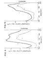
- the solid line of Fig. 4 is the action spectrum of photocurrent through a vapor-deposited zinc naphthalocyanine (in formula II, M is Zn) film.
- FIG. 4 is an absorption spectrum of a similar zinc naphthalocyanine film.
- the solid line of Fig. 5 is the action spectrum of photocurrent flow through a vapor-deposited vanadyl naphthalocyanine (in formula (II), M is OV) film.
- the broken line of Fig. 5 is an absorption spectrum of a similar vanadyl naphthalocyanine film.
- Fig. 6 shows an absorption spectrum of a vapor-deposited chloroindium naphthalocyanine (in formula (II), M is ClIn) film.
- Fig. 7 shows an absorption spectrum of a vapor-deposited chloroaluminum naphthalocyanine (in formula (II), M is ClAl) film. Meaning of symbols: 1 --- NESA film, 2 --- Glass plate, 3 --- Photoconductive layer, 4 --- Al film
- the naphthalocyanine compound of formula (I) used in the present inventive electrophotographic plate can be synthesized, for instance, by heating 2,3-dicyanonaphthalene in a sodium amyloxide-amyl alcohol mixture in the presence of a catalytic amount of ammonium molybdate under reflux for about 5 hours, and hydrolyzing the resulting sodium naphthalocyanine.
- the naphthalocyanine compound of formula (II) can be synthesized in the following manner according to the known method described in Zhurnal Obshchei Khimii, Vol. 39, p. 2554. That is, the naphthalocyanine compound of formula (II) wherein M is a metal, metal oxide, or metal halide can be obtained by reacting 2,3-dicyanonaphthalene with the corresponding metal or metal salt at about 240°C for about 2.5 hours in the presence of a catalytic amount of ammonium molybdate or by reacting 1,3-diiminobenzo[f]isoindoline, which is derived from 2,3-dicyanonaphthalene, with the corresponding metal or metal salt at about 220°C for about 2.5 hours.
- the above metal or metal salt to react is exemplified by CuCl, CuCl2, Zn, Mg, TiCl4, VCl3, AlCl3, GaCl3, InCl3, SiCl4, GeCl, and SnCl4. These reactions can be carried out with or without using a high boiling solvent such as quinoline, tetralin, 1-chloronaphthalene, 1-bromonaphthalene, or urea.
- a high boiling solvent such as quinoline, tetralin, 1-chloronaphthalene, 1-bromonaphthalene, or urea.
- naphthalocyanine compounds of the formula (I) or (II) are copper naphthalocyanine, zinc naphthalocyanine, oxytitanium naphthalocyanine, vanadyl naphthalocyanine, chloroaluminum naphthalocyanine, chlorogallium naphthalocyanine, chloroindium naphthalocyanine, metal-free naphthalocyanine and the like.
- naphthalocyanine compounds are copper naphthalocyanine, zinc naphthalocyanine, vanadyl naphthalocyanine, chloroindium naphthalocyanine, chloroaluminum naphthalocyanine, metal-free naphthalocyanine and the like.
- the naphthalocyanine compound of formula (I) or (II) When irradiated with light, the naphthalocyanine compound of formula (I) or (II) generates electric charge.
- the present inventive electrophotographic plate is provided with a photoconductive layer on an electroconductive support.
- the electroconductive supporting substrate is formed of a conductor such as; a paper or plastic film given conductivity by suitable treatment; plastic film overlaid with an aluminum foil or other metal foil; aluminum plate; or aluminum drum.
- a conductor such as; a paper or plastic film given conductivity by suitable treatment; plastic film overlaid with an aluminum foil or other metal foil; aluminum plate; or aluminum drum.
- the photoconductive layer is a film containing an organic photoconductive material, such as a coat of organic photoconductive material, a coat containing an organic photoconductive material and a binder, or a composite coat consisting of a charge generation layer and a charge transport layer.
- an organic photoconductive material such as a coat of organic photoconductive material, a coat containing an organic photoconductive material and a binder, or a composite coat consisting of a charge generation layer and a charge transport layer.
- a naphthalocyanine compound of formula (I) or (II) is used as an essential component and one or more known organic photoconductive materials may be used jointly therewith. It is preferable to use a charge transport material jointly with the naphthalocyanine compound of formula (I) or (II) or therewith along with a charge generation organic pigment.
- the charge generation layer contains said naphthalocyanine compound or a charge generation organic pigment in addition thereto while the charge transport layer contains a charge transport material.
- Suitable charge generation organic pigments include those known to generate electric charge, such as pigments of an azoxybenzene group, disazo group, trisazo group, benzimidazole group, polycyclic quinone group, indigoid group, quinacridone group, perylene group, methine group, and metal-free and metal-containing phthalocyanine groups having various crystal structures, e.g. ⁇ -, ⁇ -, ⁇ -, ⁇ -, and ⁇ -forms.
- the use of these pigments as a charge generation material is disclosed, for example, in British Patent Nos. 1,370,197; 1,337,222; 1,337,224; and 1,402,967; U.S. Patent Nos. 3,887,366; 3,838,084; 3,824,099; and 4,028,102; Canadian Patent No. 1,007,095; and German Patent Offen. No. 2,260,540.
- metal-free phthalocyanine pigments of ⁇ -, ⁇ ′-, ⁇ -, and ⁇ ′- forms can also be used. Besides these pigments, any organic pigment may be used that produces charge carriers on light irradiation.
- Suitable charge transport materials include; macromolecular compounds, e.g. poly-N-vinylcarbazole, halogenated poly-N-vinylcarbazole, polyvinylpyrene, polyvinylindoloquinoxaline, polyvinylbenzothiophene, polyvinylanthracene, polyvinylacridine, and polyvinylpyrazoline; and low molecular compounds, e.g.
- fluorenone fluorene, fluorene, 2,7-dinitro-9-fluorenone, 4H-indeno(1,2,6)- thiophene-4-one, 3,7-dinitrodibenzophenone-5-oxide, 1-bromopyrene, 2-phenylpyrene, carbazole, N-ethylcarbazole, 3-phenylcarbazole, 3-(N-methyl-N-phenylhydrazone)methyl-g-ethylcarbazole, 2-phenylindole, 2-phenylnaphthalene, oxadiazole, 2,5-bis(4-diethylaminophenyl)-1,3,4-oxadiazole, 1-phenyl-3-(4-diethylaminostyryl)-5-(4-diethylaminostyryl)-5-(4-diethylaminophenyl)pyrazoline, 1-phenyl-3-(p-dieth
- the mixing ratio of the former to the latter is desired to be from 10/1 to 2/1 by weight.
- a binder may or may not be added.
- the amount of binder to use is desirably up to 500% by weight based on the total amount of these compounds (the naphthalocyanine compound, charge generation organic pigment, and charge transport material).
- a binder is added desirably in an amount of at least 30% by weight.
- no charge transport material is used, a binder may also be added in a similar amount. Binders can be used jointly with additives, as occasion demands, which include plasticizers, flow improvers, and pinhole inhibitors.
- the charge generation layer contains the naphthalocyanine compound or this and a charge generation organic pigment and preferably may contain further a binder in an amount of up to 500% by weight based on the organic pigments and moreover the abovementioned additive in an amount of up to 5% by weight based on the amount of the naphthalocyanine compound or on the total amount of this compound and the organic pigment.
- the charge transport layer contains the above-mentioned charge transport material and preferably may contain further a binder in an amount of up to 500% by weight based on the charge transport material.
- the charge transport material is a low molecular compound
- a binder is desirably added in an amount of at least 50% by weight based on the low molecular compound.
- the charge transport layer may contain the above-mentioned additive in an amount of up to 5% by weight based on the charge transport material.
- Binders usable in all the cases stated above include silicone resin, polyamide resin, polyurethane resin, polyester resin, epoxy resin, polyketone resin, polycarbonate resin, polyacrylic resin, polystyrene resin, styrene-butadiene copolymer, polymethyl methacrylate resin, polyvinyl chloride, ethylene-vinyl acetate copolymer, vinyl chloride-vinyl acetate copolymer, polyacrylamide resin, polyvinylcarbazole, polyvinylpyrazoline, polyvinylpyrene, etc.
- Thermosetting resins and photosetting resins can also be used that can be crosslinked by heating and/or light irradiation.
- any resin may be used that is an insulator and can form a coating film under ordinary conditions or can be cured with heat and/or light to form a coating film.
- Suitable plasticizers include halogenated paraffin, dimethylnaphthalene, dibutyl phthalate, etc.
- Suitable flow improvers include Modaflow (tradename, available from Monsanto Co.), Acronal (tradename, available from BASF, A.G.), etc.
- Suitable pinhole inhibitors include benzoin, dimethyl phthalate, etc. These additives are suitably chosen and may be used in suitable amounts.
- the electrophotographic plate of the invention comprises a photoconductive layer formed on an electro conductive layer, as stated before.
- the photoconductive layer is desired to have a thickness of 5 to 50 ⁇ m.
- the charge generation layer is formed to a thickness of desirably from 0.001 to 10 ⁇ m, preferably from 0.2 to 5 ⁇ m. A thinner charge generation layer than 0.001 ⁇ m is difficult to form uniformly.
- the thickness of the charge transport layer is desirably from 5 to 50 ⁇ m, preferably from 8 to 20 ⁇ m. When this thickness is less than 5 ⁇ m, the initial potential will be undesirably low. When thickness exceeds 50 ⁇ m, the sensitivity tends to be lowered.
- a suitable method is the vapor deposition of a photoconductive material on the conductive layer.
- Another method comprises dissolving or dispersing uniformly an organic photoconductive material and, if necessary, other ingredients in a solvent, and applying the solution or dispersion on the conductive layer, followed by drying.
- the solvent is selected from; ketones, e.g. acetone and methyl ethyl ketone; ethers, e.g. tetrahydrofuran; aromatic hydrocarbons, e.g. toluene and xylene; halogenated hydrocarbons, e.g.
- the coating can be carried out by spin coating, dip coating, or other methods.
- the charge generation layer and the charge transport layer can also be formed in the same manner. In this case, either of these layers may be the upper layer. It is also allowed to interpose a charge generation layer between two charge transport layers.
- the present inventive naphthalocyanine compound In the vacuum deposition of the present inventive naphthalocyanine compound, it is desirable to heat the compound under a high vacuum of 10 ⁇ 5 to 10 ⁇ 6 mm Hg.
- the application of the present naphthalocyanine compound by spin coating is desirably carried out as follows: The compound is dispersed in a halogenated solvent such as chloroform or in a nonpolar solvent such as toluene to prepare a coating liquid and this liquid is applied by spin coating at a revolution of 3000 to 7000 rpm.
- the dip coating is desirably carried out as follows:
- the present naphthalocyanine compound is dispersed in a polar solvent such as methanol or dimethylformamide by using a ball mill or a supersonic wave to prepare a coating liquid and the conductive substrate is dipped in this coating liquid.
- the electrophotographic plate of the invention may be provided additionally with a thin bond layer or barrier layer directly over the conductive layer and also may have a protective layer at the top.
- a protective coating may be formed according to the coating and drying procedure of forming the photoconductive layer.
- FIG. 1 is a plane view of the cell and Fig. 2 is a cross-sectional view taken on line a-a′ of Fig. 1.
- a glass plate 2 supporting an NESA film 1 (about 1 cm wide) was fixed in place in a vacuum deposition chamber. Copper naphthalocyanine was placed in a vacuum-evaporation boat made of tungsten, and heated in the vacuum deposition chamber at temperatures of 550-650°C under a vacuum of 3 ⁇ 10 ⁇ 6 Torr, thereby depositing a photoconductive layer 3 on the NESA film 1 to cover it with the photoconductive layer except that a portion of the NESA film and a portion of the glass plate were uncovered. Then, aluminum was vapor-deposited on the portions of the photoconductive layer and of the glass plate to form a 1-cm wide and about 300- ⁇ thick Al layer 4 across the surface of the photoconductive layer.
- Fig. 3 shows the action spectrum obtained by plotting each quantum yield vs. the wavelength.
- the copper naphthalocyanine film formed by vapor deposition was about 2500 ⁇ thick.
- Copper naphthalocyanine that is, a compound of formula (II) wherein M is Cu, synthesized in Preparation Example 2 was vacuum-deposited on an aluminum-metalized substrate by electric resistance heating under a vacuum of 3 ⁇ 10 ⁇ 6 mm Hg to form a charge generation layer 3000 ⁇ thick.
- a solution of 5 g of 1-phenyl-3-(p-diethylaminostyryl)-5-(p-diethylaminophenyl)pyrazoline and 10 g of a polycarbonate resin in 85 g of a 1:1 methylene chloride-1,1,2-trichloroethane mixture was applied by dip coating on the charge generation layer formed on the substrate, and was dried at 120°C for 30 minutes, thereby forming a charge transport layer 15 ⁇ m thick.
- the thus prepared photosensitive member was given negative charge by a 5-KV corona discharge using an electrostatic charging test machine (supplied Kawaguchi Denki Co., Ltd.). Then, the photosensitive member was exposed to monochromatic light produced by filtering rays from a halogen lamp through a monochrometer (supplied by Ritsu Oyokogaku Co., Ltd.), where the decay of surface potential on light exposure was measured on this photosensitive member.
- the half-decay exposure quantity (the product of time and light intensity to halve the initial surface potential) was 15 mJ/m2 when this photosensitive member was exposed to monochromatic near-infrared light of 800 nm wavelength.
- a charge generation layer was formed by vacuum deposition of zinc naphthalocyanine, that is, a compound of formula (II) wherein M is Zn, synthesized in Preparatipn Example 3.
- a charge generation layer was formed by vacuum deposition of vanadyl naphthalocyanine, that is, a compound of formula (II) wherein M is OV, synthesized in Preparation Example 4.
- a solution of 5 g of 1-phenyl-3-(p-diethylaminostyryl)-5-(p-diethylaminophenyl)pyrazoline and 10 g of a polycarbonate resin in 85 g of a 1:1 methylene chloride-1,1,2-trichloroethane mixture was applied by dip coating on the charge generation layer formed on the substrate, and was dried at 120°C for 30 minutes, thereby forming a charge transport layer 15 ⁇ m thick.
- a charge generation layer was formed by vacuum deposition of chloroindium naphthalocyanine, that is, a compound of formula (II) wherein M is ClIn, synthesized in Preparation Example 5.
- a solution of 5 g of 1-phenyl-3-(p-diethylaminostyryl)-5-(p-diethylaminophenyl)pyrazoline and 10 g of a polycarbonate resin in 85 g of a 1:1 methylene chloride-1,1,2-trichloroethane mixture was applied by dip coating on the charge generation layer formed on the substrate, and was dried at 120°C for 30 minutes, thereby forming a charge transport layer 15 ⁇ m thick.
- a charge generation layer was formed by vacuum deposition of chloroaluminum naphthalocyanine, that is, a compound of formula (II) wherein M is ClAl, synthesized in Preparation Example 6.
- a solution of 5 g of 1-phenyl-3-(p-diethylaminostyryl)-5-(p-diethylaminophenyl)pyrazoline and 10 g of a polycarbonate resin in 85 g of a 1:1 methylene chloride-1,1,2-trichloroethane mixture was applied by dip coating on the charge generation layer formed on the substrate, and was dried at 120°C for 30 minutes, thereby forming a charge transport layer of 15 ⁇ m thick.
- Vacuum deposition of metal-free phthalocyanine on an aluminum-metalized substrate was carried out under a vacuum of 2 ⁇ 10 ⁇ 5 mm Hg, and a photosensitive member similar to that of Example 1 was prepared. Under the same conditions the decay of surface potential on light exposure was measured on this photosensitive member. The result indicated that the half-decay exposure quantity was 3000 mJ/m2 for monochromatic light of 800 nm wavelength. Thus, this photosensitive member was much inferior in sensitivity to those of Examples 1-5 wherein naphthalocyanine compounds of formula (1) or (II) were used.
- metal naphthalocyanines and metal-free naphthalocyanine prepared before were dispersed each in a binder, a charge generation layer was formed from the resulting dispersion, and a charge transport layer was formed on the charge generation layer by using the following materials.
- the thus prepared complex type photosensitive members (100 mm ⁇ 70 mm) were evaluated for electrophotographic characteristics.
- Hydrazone derivative p-Dimethylamino-o-ethoxybenzaldehyde diphenylhydrazone (HYZ) having the following structure:
- Silicone varnish KR-255 (supplied by Shinetsu Chemical Industry Co., Ltd.) or Polycarbonate resin: IUPILON S-2000 (supplied by Mitsubishi Gas Chemical Co., Inc.)
- An electrophotographic plates was prepared according to the procedure of Examples 6-11 but using bis(trihexylsiloxy)silicon naphthalocyanine as a charge generation material.
- An electrophotographic plates was prepared according to the procedure of Examples 6-11 but using ⁇ -form phthalocyanine (supplied by BASF A.G.) as a charge generation material.
- Electrophotographic characteristics of the plates prepared in Examples 6-11 and Comparative Examples 2 and 3 were measured by using the above-mentioned electrostatic charging test machine (model SP-428, supplied by Kawaguchi Denki Co., Ltd.). Results of the measurement are shown in Table 1.
- initial potential V0 is the potential given to the surface of the plates attached onto the rotable disk of SP-428, by a -5 KV corona discharge for 10 seconds while rotating the disk at 1000 rpm
- half-decay exposure quantity E50 is the energy of light (product of light intensity and time) incident thereafter on a unit area of the plates until the initial potential V0 was halved by exposure to monochromatic light of 800 nm wavelength which was produced by filtering rays from a halogen lamp through a monochrometer (supplied by Ritsu Oyokogaku Co., Ltd.)
- residual potential V R is the potential remaining on the plate after exposure to the monochromatic light for 60 seconds.
- the present inventive electrophotographic plates show great absorption at around 800 nm and have high sensitivity to rays of these long wavelengths without being treated with any shifting agent, hence exhibiting excellent effects when used in particular in laser beam printers.
- the present inventive photosensitive members can also be applied favorably to facsimiles, printers provided with LED light sources, and moreover to other optical recording devices provided with diode laser light sources.
Landscapes
- Physics & Mathematics (AREA)
- General Physics & Mathematics (AREA)
- Photoreceptors In Electrophotography (AREA)
- Nitrogen Condensed Heterocyclic Rings (AREA)
Applications Claiming Priority (2)
| Application Number | Priority Date | Filing Date | Title |
|---|---|---|---|
| JP9904387 | 1987-04-22 | ||
| JP99043/87 | 1987-04-22 |
Publications (3)
| Publication Number | Publication Date |
|---|---|
| EP0288876A2 true EP0288876A2 (de) | 1988-11-02 |
| EP0288876A3 EP0288876A3 (en) | 1989-11-29 |
| EP0288876B1 EP0288876B1 (de) | 1994-07-20 |
Family
ID=14236461
Family Applications (1)
| Application Number | Title | Priority Date | Filing Date |
|---|---|---|---|
| EP88106213A Expired - Lifetime EP0288876B1 (de) | 1987-04-22 | 1988-04-19 | Elektrophotographische Platte |
Country Status (4)
| Country | Link |
|---|---|
| US (1) | US4842970A (de) |
| EP (1) | EP0288876B1 (de) |
| JP (1) | JPS6438753A (de) |
| DE (1) | DE3850697T2 (de) |
Cited By (1)
| Publication number | Priority date | Publication date | Assignee | Title |
|---|---|---|---|---|
| CN102096320A (zh) * | 2009-12-09 | 2011-06-15 | 富士胶片株式会社 | 着色感光性组合物、滤色器及其制造方法及液晶显示装置 |
Families Citing this family (6)
| Publication number | Priority date | Publication date | Assignee | Title |
|---|---|---|---|---|
| JP2707630B2 (ja) * | 1988-09-14 | 1998-02-04 | 三菱化学株式会社 | 電子写真感光体 |
| US5066796A (en) * | 1990-05-31 | 1991-11-19 | Xerox Corporation | Electrophotographic imaging members with bichromophoric bisazo phthalocyanine photoconductive materials |
| US5338636A (en) * | 1991-09-27 | 1994-08-16 | Fuji Xerox Co., Ltd. | Dichlorotin phthalocyanine crystal electrophotographic photoreceptor using the same, and coating composition for electrophotographic photoreceptor |
| US5310613A (en) * | 1991-12-16 | 1994-05-10 | Xerox Corporation | High sensitivity visible and infrared photoreceptor |
| EP0595255B1 (de) * | 1992-10-26 | 2001-03-28 | Dai Nippon Printing Co., Ltd. | Photoelektrischer Sensor, Informationsaufzeichnungssystem und Methode zur Informationsaufzeichnung |
| CN110419006B (zh) * | 2017-03-31 | 2022-10-14 | 京瓷办公信息系统株式会社 | 电子照相感光体和图像形成装置 |
Family Cites Families (11)
| Publication number | Priority date | Publication date | Assignee | Title |
|---|---|---|---|---|
| US4587188A (en) * | 1982-09-06 | 1986-05-06 | Oki Electric Industry Co., Ltd. | Phthalocyanine photoconductor for electrophotography |
| JPS60184565A (ja) * | 1984-03-05 | 1985-09-20 | Yamamoto Kagaku Gosei Kk | ナフタロシアニン化合物 |
| JPS6050539A (ja) * | 1983-08-31 | 1985-03-20 | Toyo Ink Mfg Co Ltd | 電子写真感光体 |
| US4492750A (en) * | 1983-10-13 | 1985-01-08 | Xerox Corporation | Ablative infrared sensitive devices containing soluble naphthalocyanine dyes |
| JPS61171771A (ja) * | 1985-01-25 | 1986-08-02 | Mitsubishi Chem Ind Ltd | 電子写真用感光体の製造方法 |
| JPS61109056A (ja) * | 1984-11-01 | 1986-05-27 | Mitsubishi Chem Ind Ltd | 積層型電子写真感光体 |
| US4725525A (en) * | 1985-02-04 | 1988-02-16 | Hoebbst Celanese Corporation | Recording information media comprising chromophores |
| JPS6247169A (ja) * | 1985-08-26 | 1987-02-28 | Oki Electric Ind Co Ltd | 光センサ |
| US4749637A (en) * | 1986-04-24 | 1988-06-07 | Hitachi Chemical Co., Ltd. | Electrophotographic plate with silicon naphthalocyanine |
| JPS6395460A (ja) * | 1986-10-09 | 1988-04-26 | Kao Corp | 電子写真感光体 |
| JPH0752300B2 (ja) * | 1987-03-19 | 1995-06-05 | 三菱油化株式会社 | 電子写真感光体 |
-
1988
- 1988-04-19 EP EP88106213A patent/EP0288876B1/de not_active Expired - Lifetime
- 1988-04-19 DE DE3850697T patent/DE3850697T2/de not_active Expired - Fee Related
- 1988-04-20 JP JP63097798A patent/JPS6438753A/ja active Pending
- 1988-04-20 US US07/184,027 patent/US4842970A/en not_active Expired - Fee Related
Cited By (2)
| Publication number | Priority date | Publication date | Assignee | Title |
|---|---|---|---|---|
| CN102096320A (zh) * | 2009-12-09 | 2011-06-15 | 富士胶片株式会社 | 着色感光性组合物、滤色器及其制造方法及液晶显示装置 |
| CN102096320B (zh) * | 2009-12-09 | 2014-07-16 | 富士胶片株式会社 | 着色感光性组合物、滤色器及其制造方法及液晶显示装置 |
Also Published As
| Publication number | Publication date |
|---|---|
| EP0288876B1 (de) | 1994-07-20 |
| DE3850697D1 (de) | 1994-08-25 |
| JPS6438753A (en) | 1989-02-09 |
| US4842970A (en) | 1989-06-27 |
| EP0288876A3 (en) | 1989-11-29 |
| DE3850697T2 (de) | 1994-12-15 |
Similar Documents
| Publication | Publication Date | Title |
|---|---|---|
| JPH0629975B2 (ja) | 積層型電子写真用感光体 | |
| US5304445A (en) | Phthalocyanine composition, process for preparing the same and electrophotographic photoreceptor using the same | |
| EP0277039B1 (de) | Elektrophotographische Platten, die ein metallisiertes Derivat des Naphthalocyanins enthalten | |
| EP0288876B1 (de) | Elektrophotographische Platte | |
| JP3343275B2 (ja) | フタロシアニン組成物、その製造法、これを用いた電子写真感光体および電荷発生層用塗液 | |
| US5362589A (en) | Electrophotographic photoreceptor containing phthalocyanine mixed crystals | |
| US5292604A (en) | Phthalocyanine crystal of mixed pigments and electrophotographic photoreceptor using the same | |
| JPH038539B2 (de) | ||
| JP3343268B2 (ja) | フタロシアニン組成物、その製造法およびそれを用いた電子写真感光体ならびに電荷発生層用塗液 | |
| JPH07128888A (ja) | 電子写真感光体 | |
| JP3219492B2 (ja) | 電子写真感光体 | |
| JPS61124951A (ja) | 電子写真用感光体 | |
| JPH0635215A (ja) | フタロシアニンを含有する電子写真記録材料 | |
| JPH0727245B2 (ja) | 電子写真感光体 | |
| JP3232738B2 (ja) | フタロシアニン組成物、その製造法およびそれを用いた電子写真感光体ならびに電荷発生層用塗工液 | |
| JP3343277B2 (ja) | フタロシアニン組成物中間体の製造法 | |
| JPH04362653A (ja) | 電子写真感光体 | |
| JP2875360B2 (ja) | 電子写真感光体 | |
| JPH0841373A (ja) | フタロシアニン組成物、その製造法及びそれを用いた電子写真感光体 | |
| JPH10246972A (ja) | 電子写真感光体及び電荷輸送層用塗液 | |
| JP3284637B2 (ja) | フタロシアニン組成物の製造法およびそれを用いた電子写真感光体 | |
| JPH10142818A (ja) | 電子写真感光体 | |
| JP2002251027A (ja) | フタロシアニン組成物、これを含む塗液、電子写真感光体及び電子写真感光体の製造法 | |
| JPH02178358A (ja) | 新規なフタロシアニン化合物およびそれを用いた電子写真感光体 | |
| JPH08176455A (ja) | フタロシアニン組成物の製造法、これを用いた電子写真感光体及び電荷発生層用塗液 |
Legal Events
| Date | Code | Title | Description |
|---|---|---|---|
| PUAI | Public reference made under article 153(3) epc to a published international application that has entered the european phase |
Free format text: ORIGINAL CODE: 0009012 |
|
| AK | Designated contracting states |
Kind code of ref document: A2 Designated state(s): DE GB |
|
| PUAL | Search report despatched |
Free format text: ORIGINAL CODE: 0009013 |
|
| AK | Designated contracting states |
Kind code of ref document: A3 Designated state(s): DE GB |
|
| 17P | Request for examination filed |
Effective date: 19900109 |
|
| 17Q | First examination report despatched |
Effective date: 19920401 |
|
| GRAA | (expected) grant |
Free format text: ORIGINAL CODE: 0009210 |
|
| AK | Designated contracting states |
Kind code of ref document: B1 Designated state(s): DE GB |
|
| REF | Corresponds to: |
Ref document number: 3850697 Country of ref document: DE Date of ref document: 19940825 |
|
| PLBE | No opposition filed within time limit |
Free format text: ORIGINAL CODE: 0009261 |
|
| STAA | Information on the status of an ep patent application or granted ep patent |
Free format text: STATUS: NO OPPOSITION FILED WITHIN TIME LIMIT |
|
| 26N | No opposition filed | ||
| PGFP | Annual fee paid to national office [announced via postgrant information from national office to epo] |
Ref country code: GB Payment date: 19980414 Year of fee payment: 11 |
|
| PGFP | Annual fee paid to national office [announced via postgrant information from national office to epo] |
Ref country code: DE Payment date: 19980424 Year of fee payment: 11 |
|
| PG25 | Lapsed in a contracting state [announced via postgrant information from national office to epo] |
Ref country code: GB Free format text: LAPSE BECAUSE OF NON-PAYMENT OF DUE FEES Effective date: 19990419 |
|
| GBPC | Gb: european patent ceased through non-payment of renewal fee |
Effective date: 19990419 |
|
| PG25 | Lapsed in a contracting state [announced via postgrant information from national office to epo] |
Ref country code: DE Free format text: LAPSE BECAUSE OF NON-PAYMENT OF DUE FEES Effective date: 20000201 |