EP0295457A2 - Méthode de formation d'un relief utilisant une copolymérisation greffée - Google Patents
Méthode de formation d'un relief utilisant une copolymérisation greffée Download PDFInfo
- Publication number
- EP0295457A2 EP0295457A2 EP88108157A EP88108157A EP0295457A2 EP 0295457 A2 EP0295457 A2 EP 0295457A2 EP 88108157 A EP88108157 A EP 88108157A EP 88108157 A EP88108157 A EP 88108157A EP 0295457 A2 EP0295457 A2 EP 0295457A2
- Authority
- EP
- European Patent Office
- Prior art keywords
- resist layer
- oxygen
- monomer
- atmosphere
- radiation
- Prior art date
- Legal status (The legal status is an assumption and is not a legal conclusion. Google has not performed a legal analysis and makes no representation as to the accuracy of the status listed.)
- Withdrawn
Links
Images

Classifications
-
- H—ELECTRICITY
- H05—ELECTRIC TECHNIQUES NOT OTHERWISE PROVIDED FOR
- H05K—PRINTED CIRCUITS; CASINGS OR CONSTRUCTIONAL DETAILS OF ELECTRIC APPARATUS; MANUFACTURE OF ASSEMBLAGES OF ELECTRICAL COMPONENTS
- H05K3/00—Apparatus or processes for manufacturing printed circuits
- H05K3/0073—Masks not provided for in groups H05K3/02 - H05K3/46, e.g. for photomechanical production of patterned surfaces
- H05K3/0079—Masks not provided for in groups H05K3/02 - H05K3/46, e.g. for photomechanical production of patterned surfaces characterised by the method of application or removal of the mask
-
- G—PHYSICS
- G03—PHOTOGRAPHY; CINEMATOGRAPHY; ANALOGOUS TECHNIQUES USING WAVES OTHER THAN OPTICAL WAVES; ELECTROGRAPHY; HOLOGRAPHY
- G03F—PHOTOMECHANICAL PRODUCTION OF TEXTURED OR PATTERNED SURFACES, e.g. FOR PRINTING, FOR PROCESSING OF SEMICONDUCTOR DEVICES; MATERIALS THEREFOR; ORIGINALS THEREFOR; APPARATUS SPECIALLY ADAPTED THEREFOR
- G03F7/00—Photomechanical, e.g. photolithographic, production of textured or patterned surfaces, e.g. printing surfaces; Materials therefor, e.g. comprising photoresists; Apparatus specially adapted therefor
- G03F7/004—Photosensitive materials
- G03F7/027—Non-macromolecular photopolymerisable compounds having carbon-to-carbon double bonds, e.g. ethylenic compounds
-
- G—PHYSICS
- G03—PHOTOGRAPHY; CINEMATOGRAPHY; ANALOGOUS TECHNIQUES USING WAVES OTHER THAN OPTICAL WAVES; ELECTROGRAPHY; HOLOGRAPHY
- G03F—PHOTOMECHANICAL PRODUCTION OF TEXTURED OR PATTERNED SURFACES, e.g. FOR PRINTING, FOR PROCESSING OF SEMICONDUCTOR DEVICES; MATERIALS THEREFOR; ORIGINALS THEREFOR; APPARATUS SPECIALLY ADAPTED THEREFOR
- G03F7/00—Photomechanical, e.g. photolithographic, production of textured or patterned surfaces, e.g. printing surfaces; Materials therefor, e.g. comprising photoresists; Apparatus specially adapted therefor
- G03F7/26—Processing photosensitive materials; Apparatus therefor
- G03F7/38—Treatment before imagewise removal, e.g. prebaking
-
- H—ELECTRICITY
- H05—ELECTRIC TECHNIQUES NOT OTHERWISE PROVIDED FOR
- H05K—PRINTED CIRCUITS; CASINGS OR CONSTRUCTIONAL DETAILS OF ELECTRIC APPARATUS; MANUFACTURE OF ASSEMBLAGES OF ELECTRICAL COMPONENTS
- H05K2203/00—Indexing scheme relating to apparatus or processes for manufacturing printed circuits covered by H05K3/00
- H05K2203/05—Patterning and lithography; Masks; Details of resist
- H05K2203/0502—Patterning and lithography
- H05K2203/0511—Diffusion patterning
-
- H—ELECTRICITY
- H05—ELECTRIC TECHNIQUES NOT OTHERWISE PROVIDED FOR
- H05K—PRINTED CIRCUITS; CASINGS OR CONSTRUCTIONAL DETAILS OF ELECTRIC APPARATUS; MANUFACTURE OF ASSEMBLAGES OF ELECTRICAL COMPONENTS
- H05K2203/00—Indexing scheme relating to apparatus or processes for manufacturing printed circuits covered by H05K3/00
- H05K2203/08—Treatments involving gases
- H05K2203/086—Using an inert gas
-
- H—ELECTRICITY
- H05—ELECTRIC TECHNIQUES NOT OTHERWISE PROVIDED FOR
- H05K—PRINTED CIRCUITS; CASINGS OR CONSTRUCTIONAL DETAILS OF ELECTRIC APPARATUS; MANUFACTURE OF ASSEMBLAGES OF ELECTRICAL COMPONENTS
- H05K2203/00—Indexing scheme relating to apparatus or processes for manufacturing printed circuits covered by H05K3/00
- H05K2203/08—Treatments involving gases
- H05K2203/087—Using a reactive gas
-
- Y—GENERAL TAGGING OF NEW TECHNOLOGICAL DEVELOPMENTS; GENERAL TAGGING OF CROSS-SECTIONAL TECHNOLOGIES SPANNING OVER SEVERAL SECTIONS OF THE IPC; TECHNICAL SUBJECTS COVERED BY FORMER USPC CROSS-REFERENCE ART COLLECTIONS [XRACs] AND DIGESTS
- Y10—TECHNICAL SUBJECTS COVERED BY FORMER USPC
- Y10S—TECHNICAL SUBJECTS COVERED BY FORMER USPC CROSS-REFERENCE ART COLLECTIONS [XRACs] AND DIGESTS
- Y10S430/00—Radiation imagery chemistry: process, composition, or product thereof
- Y10S430/167—X-ray
- Y10S430/168—X-ray exposure process
Definitions
- the present invention relates to lithography in which light or X ray (hereinafter generically referred to as a "radiation") is used and particularly to X ray lithography by using graft copolymerization which advantageously exhibits a high throughput.
- a radiation light or X ray
- the exposure equipment should purposely be evacuated to produce a vacuum exposure atmosphere or should be provided with some means for replacing the atmosphere with an inactive gas. Further, the above-described control of the atmosphere raised a problem with respect to a lowering in the throughput of the lighography.
- an object of the prevent invention is to provide a method for forming a pattern by using graft copolymerization which enables a marked reduction in the time taken for the exposure.
- the above-described object can be attained by enabling graft copolymerization of a compound formed in a resist with a monomer through exposure in an oxygen-containing atmosphere, typically in the air.
- a polymer used as a resist etc. is oxidized upon being exposed to a radiation in the presence of oxygen to form a peroxide.
- the peroxide is known to be very unstable and tend to be easily decomposed when heated.
- the peroxide heated in an atmosphere free from oxygen is immediately decomposed to produce a radical. Therefore, it is possible to conduct graft copolymerization through contact thereof with a monomer simultaneously with or after the heat treatment.
- a substrate to be worked (4) such as a semiconductor wafer
- a resist layer (3) having a thickness of 1 ⁇ m
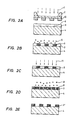
- a polymer radical (6) produced within the resist layer (3) through exposure to the X ray (1) reacted with an oxygen molecule (5) to form a peroxide (7) (see Fig. lA).
- the resist layer (3) was heated at a temperature of 40 to 110°C in an atmosphere free from oxygen, typically in vacuo, to decompose the peroxide (7) (decomposing process) while an acrylic acid monomer (8) was introduced into the system, thereby forming a graft copolymer (9) in a period of 30 min (graft copolymerization process) (see Fig. lB).
- the portion of the resist layer (3) which remained ungrafted was dissolved away with a developer comprising 2-methoxyethyl acetate, thereby forming a negative pattern (3′) (development process) (see Fig. 1C).
- a simple heat. treatment has enabled an X ray graft reaction in the air by making use of PPhMA having excellent dry etching resistance.
- the peroxide (7) may be decomposed by an infrared or radiation-induced chemical reaction.
- the decomposing process may be conducted simultaneously with the grafting process.
- a positive pattern may be formed by dissolving away, in the development process, the portion of the resist layer which has been graft polymerized. This can be attained by using a properly selected developer.
- MES-X manufactured by Japan Synthetic Rubber Co., Ltd.
- a substrate to be worked (4) to form a resist layer (3) having a thickness of 1 ⁇ m
- a resist layer (3) having a thickness of 1 ⁇ m
- the ultraviolet ray (11) was a far ultraviolet ray (wavelength: 200 to 300 nm) from a Xe lamp as a light source.
- the exposure dosage was about 50 mJ/cm2.
- the exposure of the whole surface of the resist layer (3) to the ultraviolet ray (11) brought about a remarkable decrease in the radical density of the resist layer (3) at the portion containing the peroxide (7) formed therein, i.e., at the portion exposed to the X ray (1).
- the radical density was remarkably increased at the portion free from the peroxide (7), i.e., at the portion unexposed to the X ray (1).
- an acrylic monomer (8) was introduced into the system in an atmosphere free from oxygen to form a grafted polymer (9) in a period of 30 min at the portion unexposed to the X ray (grafting process) (see Fig. 2D).
- the portion of the resist layer (3) which remained ungrafted was dissolved away with a developer comprising a mixed solution composed of ethyl cellosolve and cyclohexane, thereby forming a positive pattern (development process) (see Fig. 2E).
- the exposure process may be conducted simultaneously with the grafting process.
- the exposure process may also be conducted by making use of an electron beam or an X ray.
- a negative pattern may be formed by dissolving away, in the development process, the portion of the resist layer which has been graft polymerized. This can be attained by using a properly selected developer. Moreover, a combination of the use of a resist consisting of only an organic compound with the use of a metal-containing organic compound graft-polymerizable with the resist enables the development by etching with an oxygen plasma or the like.
- Example 2 has enabled the formation of a positive resist pattern which could not be obtained in the prior art.
- the exposure for radiation-induced graft copolymerization can be conducted in the air, which enables not only a marked decrease in the exposure throughput but also simplification of the exposure apparatus.
Landscapes
- Physics & Mathematics (AREA)
- Engineering & Computer Science (AREA)
- General Physics & Mathematics (AREA)
- Manufacturing & Machinery (AREA)
- Microelectronics & Electronic Packaging (AREA)
- Spectroscopy & Molecular Physics (AREA)
- Photosensitive Polymer And Photoresist Processing (AREA)
- Exposure And Positioning Against Photoresist Photosensitive Materials (AREA)
Applications Claiming Priority (4)
| Application Number | Priority Date | Filing Date | Title |
|---|---|---|---|
| JP131129/87 | 1987-05-29 | ||
| JP13112987A JPS63298241A (ja) | 1987-05-29 | 1987-05-29 | パタ−ン形成方法 |
| JP62171145A JPS6415918A (en) | 1987-07-10 | 1987-07-10 | Forming method of pattern |
| JP171145/87 | 1987-07-10 |
Publications (2)
| Publication Number | Publication Date |
|---|---|
| EP0295457A2 true EP0295457A2 (fr) | 1988-12-21 |
| EP0295457A3 EP0295457A3 (fr) | 1990-06-13 |
Family
ID=26466058
Family Applications (1)
| Application Number | Title | Priority Date | Filing Date |
|---|---|---|---|
| EP88108157A Withdrawn EP0295457A3 (fr) | 1987-05-29 | 1988-05-20 | Méthode de formation d'un relief utilisant une copolymérisation greffée |
Country Status (2)
| Country | Link |
|---|---|
| US (1) | US4960676A (fr) |
| EP (1) | EP0295457A3 (fr) |
Cited By (1)
| Publication number | Priority date | Publication date | Assignee | Title |
|---|---|---|---|---|
| US4954424A (en) * | 1987-07-27 | 1990-09-04 | Hitachi, Ltd. | Pattern fabrication by radiation-induced graft copolymerization |
Families Citing this family (6)
| Publication number | Priority date | Publication date | Assignee | Title |
|---|---|---|---|---|
| JP2641497B2 (ja) * | 1988-05-27 | 1997-08-13 | 株式会社日立製作所 | パターン形成方法 |
| US5592948A (en) * | 1994-01-28 | 1997-01-14 | Gatten; Ronald A. | Self contained vial for drawing, storing, sealing and identifying a fluid sample |
| JPH08324652A (ja) * | 1995-05-31 | 1996-12-10 | Eastman Kodak Co | フィルムケース |
| MX2008014636A (es) * | 2006-05-17 | 2009-06-08 | Thiosolv L L C | Proceso para tratar una corriente de gas. |
| CA2829929C (fr) | 2011-03-14 | 2015-03-03 | Mark Anderson | Elimination du sulfure d'hydrogene de l'ammoniaque liquide |
| CN119148469B (zh) * | 2024-11-14 | 2025-01-28 | 荣芯半导体(宁波)有限公司 | 一种光刻胶层的制备方法 |
Family Cites Families (7)
| Publication number | Priority date | Publication date | Assignee | Title |
|---|---|---|---|---|
| FR2389922B1 (fr) * | 1977-05-03 | 1981-08-28 | Thomson Csf | |
| EP0103052B1 (fr) * | 1982-08-25 | 1989-07-26 | Fujitsu Limited | Méthode de formation d'une couche de résist portant une image sur un corps semi-conducteur |
| US4587203A (en) * | 1983-05-05 | 1986-05-06 | Hughes Aircraft Company | Wet process for developing styrene polymer resists for submicron lithography |
| JPS6037548A (ja) * | 1983-06-27 | 1985-02-26 | テキサス インスツルメンツ インコ−ポレイテツド | 照射線反応ネガレジストの形成方法 |
| JPS60501777A (ja) * | 1983-11-02 | 1985-10-17 | ヒユ−ズ・エアクラフト・カンパニ− | 二酸化ケイ素系グラフト重合リソグラフマスク |
| US4596761A (en) * | 1983-11-02 | 1986-06-24 | Hughes Aircraft Company | Graft polymerized SiO2 lithographic masks |
| US4657845A (en) * | 1986-01-14 | 1987-04-14 | International Business Machines Corporation | Positive tone oxygen plasma developable photoresist |
-
1988
- 1988-05-20 EP EP88108157A patent/EP0295457A3/fr not_active Withdrawn
- 1988-05-27 US US07/199,712 patent/US4960676A/en not_active Expired - Fee Related
Cited By (1)
| Publication number | Priority date | Publication date | Assignee | Title |
|---|---|---|---|---|
| US4954424A (en) * | 1987-07-27 | 1990-09-04 | Hitachi, Ltd. | Pattern fabrication by radiation-induced graft copolymerization |
Also Published As
| Publication number | Publication date |
|---|---|
| EP0295457A3 (fr) | 1990-06-13 |
| US4960676A (en) | 1990-10-02 |
Similar Documents
| Publication | Publication Date | Title |
|---|---|---|
| EP0091651B1 (fr) | Procédé de réalisation de microimages | |
| JP3317582B2 (ja) | 微細パターンの形成方法 | |
| US4806456A (en) | Dry development method for a resist film and an apparatus therefor | |
| US4649100A (en) | Production of resist images, and a suitable dry film resist | |
| JPS6085526A (ja) | 少くとも一つのパタ−ン描画工程を含む製品の製作方法 | |
| EP0017032B1 (fr) | Procédé de fabrication d'un dispositif à l'état solide par décapage différentiel par plasma des couches résistantes | |
| JPS6360891B2 (fr) | ||
| US4960676A (en) | Method for forming pattern by using graft copolymerization | |
| KR900001238B1 (ko) | 레지스트막 건조현상 방법 및 장치 | |
| EP0698825A1 (fr) | Résiste sensible à l'énergie et procédé pour fabriquer un objet en utilisant ce résiste | |
| JP2641497B2 (ja) | パターン形成方法 | |
| JP2624168B2 (ja) | パターン形成方法および電子線描画装置 | |
| EP0328655B1 (fr) | Procede de formation de modeles utilisant une reaction de polymerisation greffe induite par radiation | |
| JPS5886726A (ja) | パタ−ン形成法 | |
| KR100285384B1 (ko) | 막의 패터닝 방법 | |
| JPH08320574A (ja) | パタ−ン形成方法 | |
| JPS63298241A (ja) | パタ−ン形成方法 | |
| Choi et al. | Enhanced plasma etch resistance of acrylic acid–calcium acetate modified poly (methylmethacrylate) | |
| JPH0160551B2 (fr) | ||
| GS | iBB BBSSLLLLS S | |
| JPH02257624A (ja) | レジストパターン形成方法 | |
| JPH03182758A (ja) | 凹凸パターンの形成方法 | |
| JPH01267645A (ja) | パターン形成方法 | |
| JPH01179314A (ja) | パターン形成方法 | |
| JPH03182757A (ja) | 凹凸パターンの形成方法 |
Legal Events
| Date | Code | Title | Description |
|---|---|---|---|
| PUAI | Public reference made under article 153(3) epc to a published international application that has entered the european phase |
Free format text: ORIGINAL CODE: 0009012 |
|
| AK | Designated contracting states |
Kind code of ref document: A2 Designated state(s): DE FR GB |
|
| PUAL | Search report despatched |
Free format text: ORIGINAL CODE: 0009013 |
|
| RHK1 | Main classification (correction) |
Ipc: G03F 7/027 |
|
| RHK1 | Main classification (correction) |
Ipc: G03F 7/02 |
|
| AK | Designated contracting states |
Kind code of ref document: A3 Designated state(s): DE FR GB |
|
| 17P | Request for examination filed |
Effective date: 19901212 |
|
| 17Q | First examination report despatched |
Effective date: 19930325 |
|
| STAA | Information on the status of an ep patent application or granted ep patent |
Free format text: STATUS: THE APPLICATION IS DEEMED TO BE WITHDRAWN |
|
| 18D | Application deemed to be withdrawn |
Effective date: 19930805 |