EP0300569B1 - Verfahren zum Herstellen einer Halbleiteranordnung mit einem planarisierten Aufbau - Google Patents
Verfahren zum Herstellen einer Halbleiteranordnung mit einem planarisierten Aufbau Download PDFInfo
- Publication number
- EP0300569B1 EP0300569B1 EP88201515A EP88201515A EP0300569B1 EP 0300569 B1 EP0300569 B1 EP 0300569B1 EP 88201515 A EP88201515 A EP 88201515A EP 88201515 A EP88201515 A EP 88201515A EP 0300569 B1 EP0300569 B1 EP 0300569B1
- Authority
- EP
- European Patent Office
- Prior art keywords
- layer
- depression
- filling material
- depressions
- preplanarized
- Prior art date
- Legal status (The legal status is an assumption and is not a legal conclusion. Google has not performed a legal analysis and makes no representation as to the accuracy of the status listed.)
- Expired - Lifetime
Links
Images
Classifications
-
- H—ELECTRICITY
- H10—SEMICONDUCTOR DEVICES; ELECTRIC SOLID-STATE DEVICES NOT OTHERWISE PROVIDED FOR
- H10W—GENERIC PACKAGES, INTERCONNECTIONS, CONNECTORS OR OTHER CONSTRUCTIONAL DETAILS OF DEVICES COVERED BY CLASS H10
- H10W10/00—Isolation regions in semiconductor bodies between components of integrated devices
- H10W10/01—Manufacture or treatment
- H10W10/011—Manufacture or treatment of isolation regions comprising dielectric materials
- H10W10/014—Manufacture or treatment of isolation regions comprising dielectric materials using trench refilling with dielectric materials, e.g. shallow trench isolations
- H10W10/0143—Manufacture or treatment of isolation regions comprising dielectric materials using trench refilling with dielectric materials, e.g. shallow trench isolations comprising concurrently refilling multiple trenches having different shapes or dimensions
-
- H—ELECTRICITY
- H10—SEMICONDUCTOR DEVICES; ELECTRIC SOLID-STATE DEVICES NOT OTHERWISE PROVIDED FOR
- H10W—GENERIC PACKAGES, INTERCONNECTIONS, CONNECTORS OR OTHER CONSTRUCTIONAL DETAILS OF DEVICES COVERED BY CLASS H10
- H10W10/00—Isolation regions in semiconductor bodies between components of integrated devices
- H10W10/10—Isolation regions comprising dielectric materials
- H10W10/17—Isolation regions comprising dielectric materials formed using trench refilling with dielectric materials, e.g. shallow trench isolations
Definitions
- the invention relates to a method of manufacturing a semiconductor device, in which a depression in a surface of a semiconductor substrate is filled by covering it with a preplanarized filling layer and a further planarization layer, after which the substrate is brought into contact with an etchant, in which the planarization layer and the preplanarized filling layer are etched at substantially the same rate.
- the depression in the surface of the semiconductor substrate may be a groove etched into the substrate, but may also be a space located between conductor tracks (for example of aluminium or of polycrystalline silicon) disposed on the substrate, or it may be a window provided in an isolating layer.
- the etching treatment with the etchant in which the planarization layer and the preplanarized filling layer are etched at practically the same rate can be stopped at different instants. It may be stopped, for example, at the instant at which the surface of the semiconductor substrate is reached; the depression is then filled, while no filling material is present on the surface beside the depression.
- grooves in a silicon surface may be filled with isolating material.
- a conductor such as, for example, aluminium
- a conductor may thus be provided in grooves or in windows in an isolating layer.
- the etching treatment may also be stopped before the surface of the semiconductor substrate is reached; the depression is then filled, while a layer of the filling material is also present on the surface beside the depression.
- conductor tracks may be packed in isolating material. In all these cases, a semiconductor device having a flat planarized construction is obtained.
- a method of the kind mentioned in the opening paragraph is known from IBM-TDB, Vol. 25, No. 11 B, 1983, pp. 6129-30, in which a groove in a silicon surface is filled with silicon oxide.
- This method corresponds to the preamble of claim 1.
- the preplanarized filling layer is formed in this case in two processing steps. First the surface is covered with a first silicon oxide layer. Then a photoresist mask is provided at the area of the depression. Subsequently, the part of the first silicon oxide layer not covered with the photoresist mask is etched away. The silicon surface beside the groove is fully exposed. Also silicon oxide is removed from the groove, silicon also being exposed in an edge of the groove.
- the photoresist mask is removed and the surface is covered with a second layer of silicon oxide.
- the depression in the surface of the semiconductor substrate is filled with a comparatively flat preplanarized layer. Due to the second silicon oxide layer, not the whole groove, but only the edge thereof need be filled, at which during the etching treatment silicon oxide of the first layer was etched away. Since now considerably smaller spaces have to be filled, the second silicon oxide layer has a comparatively flat surface.
- this method has further the disadvantage that during the second deposition the very small spaces at the edge of the depression have to be filled.
- a deposition process has to be used with a very good step coverage or a silicon oxide layer must be provided which liquefies during a heat treatment then additionally to be carried out, any cavities present then disappearing.
- the silicon oxide must contain a comparatively large amount of additions, such as boron or phosphorus. Thus may be very objectionable because during the heat treatment for liquefying the silicon oxide layer this addition can diffuse into the underlying and adjacent silicon.
- Semiconductor zones doped in an undesired manner can then be formed in the silicon or zones already present therein can assume undesired properties.
- the invention has inter alia for its object to obviate the said disadvantages.
- this method is for this purpose characterized as defined in claim 1.
- a single deposition is sufficient to provide the preplanarized filling layer. Since the layer of filling material is etched away over only part of its thickness, the depression remain covered with filling material throughout their surface. At the edges of the depressions no spaces are formed, in which the underlying substrate is exposed. Since the depressions are comparatively large, it is comparatively simple to fill the depressions. Therefore, less stringent requirements need be imposed on the step coverage of the deposition process to be used. Further, the filling material need not contain further additions, as a result of which it would readily liquefy during an additional heat treatment. This additional heat treatment can be omitted. An undesired doping of the underlying and adjacent substrate is thus also counteracted.
- a flat preplanarized layer is obtained if according to the invention the process of etching the layer of filling material is continued until the layer of filling material has reached beside the depressions practically the same level as at the area of the depressions.
- the layer of filling material is formed with a top layer which can be selectively etched away and has a thickness substantially equal to the depth of the depression.
- top layer which can be selectively etched away is to be understood to mean herein a top layer which can be etched away in such a manner that the part of the filling layer located below the top layer is practically not attacked or that it can readily be ascertained by an end point detection that the part of the filling layer located below the top layer is reached.
- the etching treatment must then be stopped. If the top layer of the layer of filling material beside the depression is removed, this layer is found in practice to have reached there just the same level as at the area of the depression.
- the top layer according to the invention is provided on an intermediate layer that can be selectively etched.
- the top layer can then be selectively etched away from the intermediate layer, which in turn can be selectively etched away from a subjacent layer of the filling layer located below the intermediate layer.
- the filling layer in this case consequently consists of three sublayers: the top layer, the intermediate layer and the base layer.
- the preplanarized filling layer consists of adjacent parts of the top layer (above the depression) and the base layer (beside the depression). Since these parts are made of the same material, the next planarization treatment - in which a planarization layer is formed -can be carried out without difficulty.
- a photoresist mask is used having transverse dimensions which are smaller than those of the depressions; viewed in projection, the photoresist mask then lies within the depressions.
- a preplanarized layer is obtained, which has grooves above the edges of the depressions.
- Parts of the photoresist mask located above the depressions may also have transverse dimensions which are equal to or larger than those of the depressions.
- the filling layer will then have embossed parts located above the edges of the depressions. This form is less suitable for further planarization.
- the depression is filled homogeneously after the further planarization has been carried out. Beside the material of the preplanarized filling layer, no material of the further planarization layer is then present in the depressions.
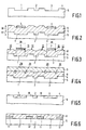
- Figures 1 to 5 show diagrammatically and in cross-section a few successive stages of manufacture of a semiconductor device by means of the method according to the invention, in which depressions 1, 2, 3 in a surface 4 of a semiconductor substrate 5 are filled. These depressions may be grooves etched into the substrate, but may also be spaces located between semiconductor tracks disposed on the substrate or windows provided in an isolating layer. The invention will be described hereinafter for grooves 1, 2, 3 etched into a semiconductor substrate 4 of monocrystalline silicon.
- the depressions 1, 2 and 3 are filled by covering the surface 4 with a filling layer of silicon oxide 6, which is preplanarized by means of a photoresist mask 7 provided at the area of the depressions 1 and 3.
- the preplanarized layer 8 is then covered with a further planarization layer 9 of, for example, photoresist HPR 204 of Hunt or with a layer of silicon oxide doped with phosphorus and boron and is then brought into contact with an etchant, in which the planarization layer 9 and the preplanarized filling layer 8 are etched at substantially the same rate.
- a further planarization layer 9 of, for example, photoresist HPR 204 of Hunt or with a layer of silicon oxide doped with phosphorus and boron is then brought into contact with an etchant, in which the planarization layer 9 and the preplanarized filling layer 8 are etched at substantially the same rate.
- the etching treatment can be stopped at different instants, for example, as indicated in Fig. 5, at the instant at which the surface 4 of the semiconductor substrate 5 is reached.
- the depressions 1, 2 and 3 are then filled, while on the surface 4 beside the depressions 1, 2 and 3 no filling material is present. If the depressions are filled with isolating material, the filled depressions 1, 2 and 3 can serve as field isolation regions in the semiconductor device. Transistors and other semiconductor elements can then be provided in a usual manner in the silicon regions 10 located between these isolation regions. If the depressions 1, 2 and 3 are grooves or windows in an isolating material, a conductor of aluminium or polycrystalline silicon can thus be provided in these grooves 1, 2 and 3.
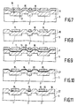
- the etching treatment can also be stopped before the surface 4 of the semiconductor substrate is reached.
- Fig. 6 such a situation is shown.
- the depressions 1, 2 and 3 are in this case the spaces located between conductor tracks 11 on the substrate 5.
- the conductor tracks are "packed” in isolating material of the filling layer 8 in this case.
- the preplanarized filling layer 8 is formed by covering the surface with a layer of filling material 6 and by then removing it beside the depressions 1, 3 over part of its thickness.
- the process of obtaining the preplanarized filling layer 8 is thus a comparatively simple process; further, each of the grooves 1, 2 and 3 can be filled homogeneously with only one kind of material.
- the process of etching the layer of filling material 6 is continued until the latter has reached on the surface 4 beside the depressions 1, 2 and 3 practically the same level 12 as the level 13 at the area of the depressions 1, 2 and 3 at which the photoresist mask 7 is provided.
- a comparatively flat preplanarized layer 8 is obtained.
- the layer of filling material 6 is formed with a top layer 15 which can be selectively etched away and has a thickness indicated by a dimension 16 and is practically equal to the depth of the depressions 1, 2, 3 indicated by a dimension 17.
- the top layer 15 consisting, for example, of polycrystalline silicon lies on a base layer 18 consisting, for example, of silicon oxide.
- the top layer 15 can be etched away from the base layer 18 in a usual manner substantially without the base layer 18 being attacked.
- the top layer 15 may also be etched, until the base layer 18 is reached this being ascertained by an end point detection, after which the etching process is stopped.
- a wet etching treatment may be used, while in the second case a dry etching treatment may be carried out in an etching plasma.
- the top layer 15 is provided according to the invention - as indicated in Fig. 9 - on an intermediate layer 20 which can be selectively etched.
- the top layer 15 of, for example, silicon oxide can then be selectively etched away from the intermediate layer 20 of, for example, silicon nitride, which in turn can be selectively etched away from the base layer 18 of, for example, silicon oxide.
- the preplanarized layer 21 is formed. If now the uncovered parts of the intermediate layer 20 are also removed, the preplanarized layer 22 has the appearance shown in Fig. 11.
- This layer 22 consists above and beside the depressions 1, 2, 3 of the same material (which was otherwise also the case with the layer 8 in Fig. 4, but in this case it was much more difficult to stop the etching process in time during the preplanarization).
- This has the advantage that, if during the further planarization (in which the planarization layer 8 is formed and is etched, this layer 9 being etched practically at the same rate as the filling layer 22) the level indicated by a dotted line 23 is reached, practically only the same materials have to be etched. This is the more the case as the layer 9 also consists of silicon oxide. In such a case, the etching process is effected in a much more homogeneous manner than in the case in which different adjacent materials have to be etched.
- the intermediate layer 20 can also be used for end point detection; the etching process can be stopped when the level indicated by a dotted line 24 is reached.
- the situation shown in Fig. 13 is then obtained, or, after the still remaining parts of the intermediate layer 20 have been removed, the situation shown in Fig. 14 is obtained.
- the situation shown in fig. 14, in which filling material of the base layer 18 is still present also on the surface 4 beside the depressions, can be entirely realized by means of dry etching in a plasma or with reactive ions. If now the etching treatment is continued in an etching bath, the flat structure shown in Fig. 5 can be obtained, the silicon regions not having been damaged during the dry etching treatment. During this treatment they were protected by the base layer 18.
- the base layer 18 must for this purpose be slightly thicker than the depth 17 of the depression 1, 2, 3.
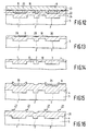
- the parts of the photoresist mask 25 located above the depressions 1 and 3 can have transverse dimensions equal to or larger than those of the depressions.
- the preplanarized layer 26 will then have embossed parts 27 above the edges of the depressions 1 and 3.
- a photoresist mask 7 is used having transverse dimensions smaller than those of the depressions 1 and 3.
- the photoresist mask 7 then lies, viewed in projection, within the depressions 1 and 3, as indicated by dotted lines 28.
- a preplanarized layer 8 is obtained, which has grooves 29 above the edges of the depressions 1 and 3.
- Such a layer is more suitable for further planarization.
- the photoresist mask 7 need be provided only above the depressions 1 and 3, within which the layer of filling material 6 has a substantially flat surface 19.
- These depressions are in practice depressions having comparatively large transverse dimensions (for example larger than 3 x 3 ⁇ m).
- Such large depressions can be filled only with difficulty in planarized form without the use of further means in a usual manner by means of a single planarization layer and an etching treatment.
- small depressions for example of about 1 x 1 ⁇ m
- the depression 2 in the Figures this can be effected satisfactorily, however.
- the depression 2 is filled by means of the planarization layer 9 and the etching treatment to be carried out after said layer has been provided. A satisfactory planarization is then obtained. It is therefore practical and simple to preplanarize the filling layer 6 only at the area of the comparatively large depressions 1 and 3.
- the single layer of filling material 6 as shown in Fig. 2 is provided in a thickness which is indicated by a dimension 30 and is at least twice the depth of the depressions 1, 2 and 3 in the surface indicated by a dimension 17. After the further planarization, the depressions 1, 2 and 3 are then filled homogeneously with filling material. In the depressions 1, 2 and 3, only material of the filling layer 6 is present.
- the depressions 1, 2 and 3 which in practice have dimensions of more than 0.5 x 0.5 ⁇ m, can be filled simply and satisfactorily by covering the surface with a layer of filling material 6 by heating the substrate 5 to a temperature of 600 to 800°C in a flow of gas comprising only tetraethyl orthosilicate and an inert gas.
- the depressions 1, 2 and 3 are filled with silicon oxide, which further does not contain substances which can diffuse into the underlying substrate 5 and can produce there an undesired doping. Phosphorus and boron are often added for filling even smaller depressions.
- Such a layer follows exactly the surface 4 so that level differences in the layer above and beside the depressions are just equal to the depth of the depressions 1, 2, 3.
- the whole filling layer but at any rate the base layer - and in the case with the intermediate layer also the top layer - is thus formed.
Landscapes
- Drying Of Semiconductors (AREA)
- Element Separation (AREA)
- Internal Circuitry In Semiconductor Integrated Circuit Devices (AREA)
Claims (7)
- Verfahren zur Herstellung einer Halbleiteranordnung, bei dem eine Vertiefung (1, 2, 3) in einer Oberfläche (4) eines Halbleitersubstrats (5) gefüllt wird, indem auf der Oberfläche (4) eine erste Schicht aus einem Füllmaterial (6) gebildet wird, eine vorplanarisierte Schicht (8, 19 22) gebildet wird, auf der vorplanarisierten Schicht (8, 19, 22) eine weitere Planarisierungsschicht (9) aus einem Füllmaterial gebildet wird und dann eine Ätzbehandlung durchgeführt wird, bei der die weitere Planarisierungsschicht (9) und die vorplanarisierte Schicht (8, 19, 22) in Kontakt mit einem Ätzmittel gebracht werden, in dem die genannte weitere Planarisierungsschicht (9) und die genannte vorplanarisierte Schicht (8, 19, 22) mit nahezu gleicher Ätzrate geätzt werden, dadurch gekennzeichnet, daß die vorplanarisierte Schicht (8, 19, 22) aus der ersten Schicht aus Füllmaterial (6) gebildet wird, indem diese Schicht (6) nur neben der Vertiefung (1, 2, 3) und nur bis auf einen Teil ihrer Dicke (30) entfernt wird, wobei die Vertiefung (1, 2, 3) auf ihrer gesamten Oberfläche mit Füllmaterial (6) bedeckt bleibt und an ihren Kanten keine Räume gebildet werden, in denen das darunterliegende Substrat (4) freigelegt wird.
- Verfahren nach Anspruch 1, dadurch gekennzeichnet, daß die erste Schicht aus Füllmaterial (6) geätzt wird, bis ihre Dicke neben der Vertiefung nahezu das gleiche Niveau erreicht wie am Ort der Vertiefung (1, 2, 3).
- Verfahren nach Anspruch 2, dadurch gekennzeichnet, daß die erste Schicht aus Füllmaterial (6) mit einer obersten Schicht (15) gebildet wird, die selektiv weggeätzt werden kann und deren Dicke (16) nahezu gleich der Tiefe der Vertiefung (1, 2, 3) ist.
- Verfahren nach Anspruch 3, dadurch gekennzeichnet, daß die oberste Schicht (15) auf einer Zwischenschicht (20) angebracht ist, die selektiv weggeätzt werden kann, und daß die genannte oberste Schicht (15) aus dem gleichen Material hergestellt ist wie die unter der Zwischenschicht (20) liegende erste Schicht aus Füllmaterial.
- Verfahren nach einem der vorstehenden Ansprüche, dadurch gekennzeichnet, daß während des Schrittes zur Ätzung der ersten Schicht aus Füllmaterial (6) eine Fotolackschicht (7) verwendet wird die, in Projektionsansicht, innerhalb der Vertiefung (1, 2, 3) liegt.
- Verfahren nach einem der vorstehenden Ansprüche, dadurch gekennzeichnet, daß die erste Schicht aus Füllmaterial (6) mit einer Dicke (30) angebracht wird, die wenigstens das Zweifache der Tiefe der Vertiefung (1, 2, 3) beträgt.
- Verfahren nach einem der vorstehenden Ansprüche, dadurch gekennzeichnet, daß die Schicht aus Füllmaterial (6) gebildet wird, indem das Substrat in einem nur Tetraethylorthosilicat und ein Inertgas enthaltenden Gasstrom auf eine Temperatur von 600 bis 800° C erhitzt wird.
Applications Claiming Priority (2)
| Application Number | Priority Date | Filing Date | Title |
|---|---|---|---|
| NL8701717 | 1987-07-21 | ||
| NL8701717A NL8701717A (nl) | 1987-07-21 | 1987-07-21 | Werkwijze voor het vervaardigen van een halfgeleiderinrichting met een geplanariseerde opbouw. |
Publications (2)
| Publication Number | Publication Date |
|---|---|
| EP0300569A1 EP0300569A1 (de) | 1989-01-25 |
| EP0300569B1 true EP0300569B1 (de) | 1994-12-28 |
Family
ID=19850350
Family Applications (1)
| Application Number | Title | Priority Date | Filing Date |
|---|---|---|---|
| EP88201515A Expired - Lifetime EP0300569B1 (de) | 1987-07-21 | 1988-07-14 | Verfahren zum Herstellen einer Halbleiteranordnung mit einem planarisierten Aufbau |
Country Status (6)
| Country | Link |
|---|---|
| US (1) | US5015602A (de) |
| EP (1) | EP0300569B1 (de) |
| JP (1) | JPS6437840A (de) |
| KR (1) | KR890003005A (de) |
| DE (1) | DE3852583T2 (de) |
| NL (1) | NL8701717A (de) |
Families Citing this family (42)
| Publication number | Priority date | Publication date | Assignee | Title |
|---|---|---|---|---|
| US4836885A (en) * | 1988-05-03 | 1989-06-06 | International Business Machines Corporation | Planarization process for wide trench isolation |
| US4954459A (en) * | 1988-05-12 | 1990-09-04 | Advanced Micro Devices, Inc. | Method of planarization of topologies in integrated circuit structures |
| US4962064A (en) * | 1988-05-12 | 1990-10-09 | Advanced Micro Devices, Inc. | Method of planarization of topologies in integrated circuit structures |
| ATE115770T1 (de) * | 1989-09-08 | 1994-12-15 | Siemens Ag | Verfahren zur globalen planarisierung von oberflächen für integrierte halbleiterschaltungen. |
| DE69004932T2 (de) * | 1989-10-25 | 1994-05-19 | Ibm | Verfahren zur Herstellung breiter mit Dielektrikum gefüllter Isolationsgraben für Halbleiteranordnungen. |
| US5173439A (en) * | 1989-10-25 | 1992-12-22 | International Business Machines Corporation | Forming wide dielectric-filled isolation trenches in semi-conductors |
| US5413966A (en) * | 1990-12-20 | 1995-05-09 | Lsi Logic Corporation | Shallow trench etch |
| US5290396A (en) * | 1991-06-06 | 1994-03-01 | Lsi Logic Corporation | Trench planarization techniques |
| US5225358A (en) * | 1991-06-06 | 1993-07-06 | Lsi Logic Corporation | Method of forming late isolation with polishing |
| US5248625A (en) * | 1991-06-06 | 1993-09-28 | Lsi Logic Corporation | Techniques for forming isolation structures |
| US5252503A (en) * | 1991-06-06 | 1993-10-12 | Lsi Logic Corporation | Techniques for forming isolation structures |
| US5382541A (en) * | 1992-08-26 | 1995-01-17 | Harris Corporation | Method for forming recessed oxide isolation containing deep and shallow trenches |
| FR2717306B1 (fr) * | 1994-03-11 | 1996-07-19 | Maryse Paoli | Procédé d'isolement de zones actives d'un substrat semi-conducteur par tranchées peu profondes, notamment étroites, et dispositif correspondant. |
| FR2717307B1 (fr) * | 1994-03-11 | 1996-07-19 | Maryse Paoli | Procede d'isolement de zones actives d'un substrat semi-conducteur par tranchees peu profondes quasi planes, et dispositif correspondant |
| US5532188A (en) * | 1994-03-30 | 1996-07-02 | Wright; Peter J. | Global planarization of multiple layers |
| US5459096A (en) * | 1994-07-05 | 1995-10-17 | Motorola Inc. | Process for fabricating a semiconductor device using dual planarization layers |
| DE19538005A1 (de) * | 1995-10-12 | 1997-04-17 | Fraunhofer Ges Forschung | Verfahren zum Erzeugen einer Grabenisolation in einem Substrat |
| US5904539A (en) * | 1996-03-21 | 1999-05-18 | Advanced Micro Devices, Inc. | Semiconductor trench isolation process resulting in a silicon mesa having enhanced mechanical and electrical properties |
| JP2000508474A (ja) * | 1996-04-10 | 2000-07-04 | アドバンスト・マイクロ・ディバイシズ・インコーポレイテッド | 改善された平坦化方法を伴う半導体トレンチアイソレーション |
| US5926713A (en) * | 1996-04-17 | 1999-07-20 | Advanced Micro Devices, Inc. | Method for achieving global planarization by forming minimum mesas in large field areas |
| US5899727A (en) | 1996-05-02 | 1999-05-04 | Advanced Micro Devices, Inc. | Method of making a semiconductor isolation region bounded by a trench and covered with an oxide to improve planarization |
| KR100236097B1 (ko) * | 1996-10-30 | 1999-12-15 | 김영환 | 반도체 장치의 격리막 형성방법 |
| US5721172A (en) * | 1996-12-02 | 1998-02-24 | Taiwan Semiconductor Manufacturing Company, Ltd. | Self-aligned polish stop layer hard masking method for forming planarized aperture fill layers |
| US5792707A (en) * | 1997-01-27 | 1998-08-11 | Chartered Semiconductor Manufacturing Ltd. | Global planarization method for inter level dielectric layers of integrated circuits |
| US6063702A (en) * | 1997-01-27 | 2000-05-16 | Chartered Semiconductor Manufacturing, Ltd. | Global planarization method for inter level dielectric layers using IDL blocks |
| US6025270A (en) * | 1997-02-03 | 2000-02-15 | Taiwan Semiconductor Manufacturing Company, Ltd. | Planarization process using tailored etchback and CMP |
| US5804490A (en) * | 1997-04-14 | 1998-09-08 | International Business Machines Corporation | Method of filling shallow trenches |
| KR100458475B1 (ko) * | 1997-06-30 | 2005-02-23 | 주식회사 하이닉스반도체 | 반도체소자의평탄화방법 |
| KR100363093B1 (ko) * | 2000-07-28 | 2002-12-05 | 삼성전자 주식회사 | 반도체 소자의 층간 절연막 평탄화 방법 |
| US6531265B2 (en) | 2000-12-14 | 2003-03-11 | International Business Machines Corporation | Method to planarize semiconductor surface |
| US6559009B2 (en) * | 2001-03-29 | 2003-05-06 | Macronix International Co. Ltd. | Method of fabricating a high-coupling ratio flash memory |
| DE10123509A1 (de) * | 2001-05-15 | 2002-11-28 | Infineon Technologies Ag | Verfahren zur Planarisierung einer Halbleiterstruktur |
| US6617241B1 (en) | 2003-01-15 | 2003-09-09 | Institute Of Microelectronics | Method of thick film planarization |
| US7323417B2 (en) * | 2004-09-21 | 2008-01-29 | Molecular Imprints, Inc. | Method of forming a recessed structure employing a reverse tone process |
| US7262070B2 (en) * | 2003-09-29 | 2007-08-28 | Intel Corporation | Method to make a weight compensating/tuning layer on a substrate |
| US7205244B2 (en) * | 2004-09-21 | 2007-04-17 | Molecular Imprints | Patterning substrates employing multi-film layers defining etch-differential interfaces |
| US7547504B2 (en) | 2004-09-21 | 2009-06-16 | Molecular Imprints, Inc. | Pattern reversal employing thick residual layers |
| US20070077763A1 (en) * | 2005-09-30 | 2007-04-05 | Molecular Imprints, Inc. | Deposition technique to planarize a multi-layer structure |
| DE102010046213B3 (de) | 2010-09-21 | 2012-02-09 | Infineon Technologies Austria Ag | Verfahren zur Herstellung eines Strukturelements und Halbleiterbauelement mit einem Strukturelement |
| US8728891B2 (en) | 2010-09-21 | 2014-05-20 | Infineon Technologies Austria Ag | Method for producing contact openings in a semiconductor body and self-aligned contact structures on a semiconductor body |
| US8409986B2 (en) * | 2011-01-11 | 2013-04-02 | Institute of Microelectronics, Chinese Academy of Sciences | Method for improving within die uniformity of metal plug chemical mechanical planarization process in gate last route |
| US11201426B2 (en) * | 2018-08-13 | 2021-12-14 | Apple Inc. | Electrical contact appearance and protection |
Family Cites Families (20)
| Publication number | Priority date | Publication date | Assignee | Title |
|---|---|---|---|---|
| US4038110A (en) * | 1974-06-17 | 1977-07-26 | Ibm Corporation | Planarization of integrated circuit surfaces through selective photoresist masking |
| US3976524A (en) * | 1974-06-17 | 1976-08-24 | Ibm Corporation | Planarization of integrated circuit surfaces through selective photoresist masking |
| US4199384A (en) * | 1979-01-29 | 1980-04-22 | Rca Corporation | Method of making a planar semiconductor on insulating substrate device utilizing the deposition of a dual dielectric layer between device islands |
| JPS5893327A (ja) * | 1981-11-30 | 1983-06-03 | Toshiba Corp | 微細加工法 |
| DE3228399A1 (de) * | 1982-07-29 | 1984-02-02 | Siemens AG, 1000 Berlin und 8000 München | Verfahren zum herstellen einer monolithisch integrierten schaltung |
| US4470874A (en) * | 1983-12-15 | 1984-09-11 | International Business Machines Corporation | Planarization of multi-level interconnected metallization system |
| US4481070A (en) * | 1984-04-04 | 1984-11-06 | Advanced Micro Devices, Inc. | Double planarization process for multilayer metallization of integrated circuit structures |
| US4594769A (en) * | 1984-06-15 | 1986-06-17 | Signetics Corporation | Method of forming insulator of selectively varying thickness on patterned conductive layer |
| US4545852A (en) * | 1984-06-20 | 1985-10-08 | Hewlett-Packard Company | Planarization of dielectric films on integrated circuits |
| US4708767A (en) * | 1984-10-05 | 1987-11-24 | Signetics Corporation | Method for providing a semiconductor device with planarized contacts |
| US4541169A (en) * | 1984-10-29 | 1985-09-17 | International Business Machines Corporation | Method for making studs for interconnecting metallization layers at different levels in a semiconductor chip |
| JPH0642482B2 (ja) * | 1984-11-15 | 1994-06-01 | 株式会社東芝 | 半導体装置の製造方法 |
| US4789760A (en) * | 1985-04-30 | 1988-12-06 | Advanced Micro Devices, Inc. | Via in a planarized dielectric and process for producing same |
| US4605470A (en) * | 1985-06-10 | 1986-08-12 | Advanced Micro Devices, Inc. | Method for interconnecting conducting layers of an integrated circuit device |
| JPS61287245A (ja) * | 1985-06-14 | 1986-12-17 | Hitachi Ltd | 多層配線法 |
| US4662064A (en) * | 1985-08-05 | 1987-05-05 | Rca Corporation | Method of forming multi-level metallization |
| JPS62169442A (ja) * | 1986-01-22 | 1987-07-25 | Nec Corp | 素子分離領域の形成方法 |
| FR2599892B1 (fr) * | 1986-06-10 | 1988-08-26 | Schiltz Andre | Procede d'aplanissement d'un substrat semiconducteur revetu d'une couche dielectrique |
| JPS6430243A (en) * | 1987-07-24 | 1989-02-01 | Matsushita Electric Industrial Co Ltd | Manufacture of semiconductor device |
| US4836885A (en) * | 1988-05-03 | 1989-06-06 | International Business Machines Corporation | Planarization process for wide trench isolation |
-
1987
- 1987-07-21 NL NL8701717A patent/NL8701717A/nl not_active Application Discontinuation
-
1988
- 1988-07-14 EP EP88201515A patent/EP0300569B1/de not_active Expired - Lifetime
- 1988-07-14 DE DE3852583T patent/DE3852583T2/de not_active Expired - Fee Related
- 1988-07-18 JP JP63177255A patent/JPS6437840A/ja active Pending
- 1988-07-21 KR KR1019880009112A patent/KR890003005A/ko not_active Ceased
-
1990
- 1990-05-10 US US07/522,490 patent/US5015602A/en not_active Expired - Fee Related
Also Published As
| Publication number | Publication date |
|---|---|
| DE3852583T2 (de) | 1995-07-13 |
| US5015602A (en) | 1991-05-14 |
| EP0300569A1 (de) | 1989-01-25 |
| JPS6437840A (en) | 1989-02-08 |
| DE3852583D1 (de) | 1995-02-09 |
| NL8701717A (nl) | 1989-02-16 |
| KR890003005A (ko) | 1989-04-12 |
Similar Documents
| Publication | Publication Date | Title |
|---|---|---|
| EP0300569B1 (de) | Verfahren zum Herstellen einer Halbleiteranordnung mit einem planarisierten Aufbau | |
| US3976524A (en) | Planarization of integrated circuit surfaces through selective photoresist masking | |
| US4663832A (en) | Method for improving the planarity and passivation in a semiconductor isolation trench arrangement | |
| EP0166207B1 (de) | Vereinfachtes Planarisationsverfahren für mit Polysilicium gefüllte Gräben | |
| EP0316550A2 (de) | Isolationszonen mit Gräben und Verfahren zu deren Herstellung | |
| US5264395A (en) | Thin SOI layer for fully depleted field effect transistors | |
| US4732658A (en) | Planarization of silicon semiconductor devices | |
| USRE38363E1 (en) | Method of forming trench isolation having polishing step and method of manufacturing semiconductor device | |
| JPH01276641A (ja) | 半導体デバイスの製造方法 | |
| EP0603097A2 (de) | Als Polierstoppschicht für die Herstellung vom Substraten von SOI-Typ verwendetes Nitrit | |
| GB2216336A (en) | Forming insulating layers on substrates | |
| US6194287B1 (en) | Shallow trench isolation (STI) method with reproducible alignment registration | |
| US6541349B2 (en) | Shallow trench isolation using non-conformal dielectric and planarizatrion | |
| US5514624A (en) | Method of manufacturing a microelectronic interlayer dielectric structure | |
| US7410873B2 (en) | Method of manufacturing a semiconductor device | |
| US6143673A (en) | Method for forming gap filling silicon oxide intermetal dielectric (IMD) layer formed employing ozone-tEOS | |
| US6270353B1 (en) | Low cost shallow trench isolation using non-conformal dielectric material | |
| US6214695B1 (en) | Method of manufacturing semiconductor device | |
| US5965938A (en) | Integrated two-tiered via-plug to improve metal lithography # 4 | |
| US6214735B1 (en) | Method for planarizing a semiconductor substrate | |
| US6204149B1 (en) | Methods of forming polished material and methods of forming isolation regions | |
| KR950014114B1 (ko) | 소자분리용 절연막 형성방법 | |
| KR0165453B1 (ko) | Y자형 트랜치를 이용한 반도체 소자의 분리 방법 | |
| KR100374682B1 (ko) | 포토레지스트 평탄화를 통해 디바이스 파라미터를균등화하기 위한 방법 | |
| KR100277858B1 (ko) | 반도체소자의 갭필링(gap filling)방법 |
Legal Events
| Date | Code | Title | Description |
|---|---|---|---|
| PUAI | Public reference made under article 153(3) epc to a published international application that has entered the european phase |
Free format text: ORIGINAL CODE: 0009012 |
|
| AK | Designated contracting states |
Kind code of ref document: A1 Designated state(s): DE FR GB IT NL |
|
| 17P | Request for examination filed |
Effective date: 19890715 |
|
| 17Q | First examination report despatched |
Effective date: 19920714 |
|
| GRAA | (expected) grant |
Free format text: ORIGINAL CODE: 0009210 |
|
| AK | Designated contracting states |
Kind code of ref document: B1 Designated state(s): DE FR GB IT NL |
|
| PG25 | Lapsed in a contracting state [announced via postgrant information from national office to epo] |
Ref country code: NL Effective date: 19941228 |
|
| REF | Corresponds to: |
Ref document number: 3852583 Country of ref document: DE Date of ref document: 19950209 |
|
| ITF | It: translation for a ep patent filed | ||
| ET | Fr: translation filed | ||
| NLV1 | Nl: lapsed or annulled due to failure to fulfill the requirements of art. 29p and 29m of the patents act | ||
| PLBE | No opposition filed within time limit |
Free format text: ORIGINAL CODE: 0009261 |
|
| STAA | Information on the status of an ep patent application or granted ep patent |
Free format text: STATUS: NO OPPOSITION FILED WITHIN TIME LIMIT |
|
| 26N | No opposition filed | ||
| PGFP | Annual fee paid to national office [announced via postgrant information from national office to epo] |
Ref country code: GB Payment date: 19960701 Year of fee payment: 9 |
|
| PGFP | Annual fee paid to national office [announced via postgrant information from national office to epo] |
Ref country code: FR Payment date: 19960724 Year of fee payment: 9 |
|
| PGFP | Annual fee paid to national office [announced via postgrant information from national office to epo] |
Ref country code: DE Payment date: 19960924 Year of fee payment: 9 |
|
| PG25 | Lapsed in a contracting state [announced via postgrant information from national office to epo] |
Ref country code: GB Free format text: LAPSE BECAUSE OF NON-PAYMENT OF DUE FEES Effective date: 19970714 |
|
| GBPC | Gb: european patent ceased through non-payment of renewal fee |
Effective date: 19970714 |
|
| PG25 | Lapsed in a contracting state [announced via postgrant information from national office to epo] |
Ref country code: FR Free format text: LAPSE BECAUSE OF NON-PAYMENT OF DUE FEES Effective date: 19980331 |
|
| PG25 | Lapsed in a contracting state [announced via postgrant information from national office to epo] |
Ref country code: DE Free format text: LAPSE BECAUSE OF NON-PAYMENT OF DUE FEES Effective date: 19980401 |
|
| REG | Reference to a national code |
Ref country code: FR Ref legal event code: ST |
|
| PG25 | Lapsed in a contracting state [announced via postgrant information from national office to epo] |
Ref country code: IT Free format text: LAPSE BECAUSE OF NON-PAYMENT OF DUE FEES;WARNING: LAPSES OF ITALIAN PATENTS WITH EFFECTIVE DATE BEFORE 2007 MAY HAVE OCCURRED AT ANY TIME BEFORE 2007. THE CORRECT EFFECTIVE DATE MAY BE DIFFERENT FROM THE ONE RECORDED. Effective date: 20050714 |