EP0301184B1 - CMOS-Referenzspannungsgenerator - Google Patents
CMOS-Referenzspannungsgenerator Download PDFInfo
- Publication number
- EP0301184B1 EP0301184B1 EP88107309A EP88107309A EP0301184B1 EP 0301184 B1 EP0301184 B1 EP 0301184B1 EP 88107309 A EP88107309 A EP 88107309A EP 88107309 A EP88107309 A EP 88107309A EP 0301184 B1 EP0301184 B1 EP 0301184B1
- Authority
- EP
- European Patent Office
- Prior art keywords
- terminal
- fet
- fet devices
- devices
- source
- Prior art date
- Legal status (The legal status is an assumption and is not a legal conclusion. Google has not performed a legal analysis and makes no representation as to the accuracy of the status listed.)
- Expired - Lifetime
Links
- 239000000758 substrate Substances 0.000 claims description 19
- 238000000034 method Methods 0.000 claims description 16
- 230000000694 effects Effects 0.000 claims description 3
- 238000005516 engineering process Methods 0.000 description 3
- 238000004519 manufacturing process Methods 0.000 description 2
- 238000004458 analytical method Methods 0.000 description 1
- 239000003990 capacitor Substances 0.000 description 1
- 239000004020 conductor Substances 0.000 description 1
- 230000014509 gene expression Effects 0.000 description 1
- 239000007943 implant Substances 0.000 description 1
- 238000005468 ion implantation Methods 0.000 description 1
- 238000004806 packaging method and process Methods 0.000 description 1
Images
Classifications
-
- G—PHYSICS
- G05—CONTROLLING; REGULATING
- G05F—SYSTEMS FOR REGULATING ELECTRIC OR MAGNETIC VARIABLES
- G05F3/00—Non-retroactive systems for regulating electric variables by using an uncontrolled element, or an uncontrolled combination of elements, such element or such combination having self-regulating properties
- G05F3/02—Regulating voltage or current
- G05F3/08—Regulating voltage or current wherein the variable is DC
- G05F3/10—Regulating voltage or current wherein the variable is DC using uncontrolled devices with non-linear characteristics
- G05F3/16—Regulating voltage or current wherein the variable is DC using uncontrolled devices with non-linear characteristics being semiconductor devices
- G05F3/20—Regulating voltage or current wherein the variable is DC using uncontrolled devices with non-linear characteristics being semiconductor devices using diode- transistor combinations
- G05F3/24—Regulating voltage or current wherein the variable is DC using uncontrolled devices with non-linear characteristics being semiconductor devices using diode- transistor combinations wherein the transistors are of the field-effect type only
- G05F3/242—Regulating voltage or current wherein the variable is DC using uncontrolled devices with non-linear characteristics being semiconductor devices using diode- transistor combinations wherein the transistors are of the field-effect type only with compensation for device parameters, e.g. channel width modulation, threshold voltage, processing, or external variations, e.g. temperature, loading, supply voltage
- G05F3/245—Regulating voltage or current wherein the variable is DC using uncontrolled devices with non-linear characteristics being semiconductor devices using diode- transistor combinations wherein the transistors are of the field-effect type only with compensation for device parameters, e.g. channel width modulation, threshold voltage, processing, or external variations, e.g. temperature, loading, supply voltage producing a voltage or current as a predetermined function of the temperature
Landscapes
- Engineering & Computer Science (AREA)
- Microelectronics & Electronic Packaging (AREA)
- Physics & Mathematics (AREA)
- Nonlinear Science (AREA)
- Electromagnetism (AREA)
- General Physics & Mathematics (AREA)
- Radar, Positioning & Navigation (AREA)
- Automation & Control Theory (AREA)
- Control Of Electrical Variables (AREA)
Claims (9)
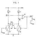
- Einrichtung zum Erzeugen einer Referenzspannung, die folgendes aufweist:
ein erstes FET-Bauelement (Q1) und ein zweites FET-Bauelement (Q2), wobei jedes Bauelement einen Steueranschluß einen Drain-Anschluß, einen Source-Anschluß und einen Substratanschluß aufweist und der Substratanschluß und der Source-Anschluß des zweiten FET-Bauelements (Q2) miteinander verbunden sind,
einen Operationsverstärker (10) mit einem Anschluß (A) für einen positiven Eingang, der mit dem Source-Anschluß des ersten FET-Bauelements (Q1) verbunden ist, mit einem Anschluß (B) für einen negativen Eingang, der mit dem Source-Anschluß des zweiten FET-Bauelements (Q2) verbunden ist und mit einem Ausgangsanschluß, der mit dem Steueranschluß des zweiten FET-Bauelements (Q2) verbunden ist und
ein erstes Vorspannungsnetzwerk zum Erzeugen einer ersten Referenzspannung (VACG), das mit dem Steueranschluß des ersten FET-Bauelements (Q1) verbunden ist,
wobei die Einrichtung dadurch gekennzeichnet ist, daß:
das erste und das zweite FET-Bauelement (Q1, Q2) identische FET-Bauelemente sind,
ein zweites Vorspannungsnetzwerk eine zweite Referenzspannung (VBS) erzeugt und zwischen dem Source- und dem Substratanschluß des ersten FET-Bauelements geschaltet ist und das erste und zweite Strommittel identische Ströme erzeugen und an die entsprechende Source-Elektroden des ersten und des zweiten FET-Bauelements (Q1, Q2) geschaltet sind,
wodurch der Operationsverstärker eine Ausgangsreferenzspannung liefert, die frei von den Effekten einer Verfahrens- und Temperaturänderung ist. - Einrichtung nach Anspruch 1, die ferner eine mit den Strommitteln verbundene Einschienenspannungsversorgung (VDD) aufweist.
- Einrichtung nach Anspruch 1 oder 2, bei welcher das erste und zweite FET-Bauelement der p-Kanal-Anreicherungsart angehören.
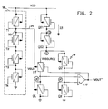
- Einrichtung zum Erzeugen einer Referenzspannung, die folgendes aufweist:
ein erstes FET-Bauelement (Q'1) und ein zweites FET-Bauelement (Q'2), wobei jedes Bauelement einen Steueranschluß einen Drain-Anschluß, einen Source-Anschluß und einen Substratanschluß aufweist und der Substratanschluß und der Source-Anschluß des zweiten FET-Bauelements (Q'2) miteinander verbunden sind,
einen Operationsverstärker 10' mit einem Anschluß (A') für einen positiven Eingang, der mit dem Drain-Anschluß des zweiten FET-Bauelements (Q'2) verbunden ist, mit einem Anschluß (B') für einen negativen Eingang, der mit dem Drain-Anschluß des ersten FET-Bauelements (Q'1) verbunden ist und mit einem Ausgangsanschluß, der mit dem Steueranschluß des ersten FET-Bauelements (Q'1) verbunden ist,
wobei die Einrichtung dadurch gekennzeichnet ist, daß
das erste und das zweite FET-Bauelement (Q'1, Q'2) identische FET-Bauelemente sind,
jedes eines ersten Paares stromeinstellender FET-Bauelemente (QL, QR) zwischen den Drain-Anschluß und dem Massepotential des ersten und des zweiten FET-Bauelements (Q'1, Q'2) geschaltet ist,
ein zweites Paar spannungseinstellender FET-Bauelemente (QS1, QS2) in Reihe zwischen beiden Source-Anschlüssen des ersten und des zweiten FET-Bauelements (Q'1, Q'2) und einer Energieversorgungsspannung (VDD) geschaltet ist und
eine Mehrzahl von FET-Bauelementen (T₁, T₂, T₃, T₄) in Reihe zwischen dem Massepotential und der Energieversorgungsspannung (VDD) geschaltet ist, wobei ein ausgewählter Knoten zwischen zwei aus der Mehrzahl von FET-Bauelementen mit dem Substratanschluß des ersten FET-Bauelements (Q'1) verbunden ist,
wodurch der Operationsverstärker eine Ausgangsreferenzspannung liefert, die frei von den Effekten einer Verfahrens- und Temperaturänderung ist. - Einrichtung nach Anspruch 4, bei welcher die FET-Bauelemente der p-Kanal-Anreicherungsart angehören.
- Einrichtung nach Anspruch 4 oder 5, bei welcher die W/L-Verhältnisse des Paares spannungseinstellender FET-Bauelemente (QS1, QS2) dieselben sind.
- Einrichtung nach Anspruch 6, bei welcher das W/L-Verhältnis des Paares spannungseinstellender FET-Bauelemente (QS1, QS1) das doppelte des W/L-Verhältnisses des Paares stromeinstellender FET-Bauelemente (QL, QR) ist.
- Einrichtung nach irgend einem der vorgehenden Ansprüche 4 bis 7, bei welcher das W/L-Verhältnis des ersten (Q1') und des zweiten (Q2') FET-Bauelements und des Paares stromeinstellender FET-Bauelemente (QL, QR) gleich ist.
- Einrichtung nach Anspruch 8, bei welcher die FET-Bauelemente dieser Mehrzahl Bauelemente der P-Kanal-Anreicherungsbetriebsart sind, wobei der Substratanschluß jedes Bauelementes mit dessen Source-Anschluß und der Gate-Anschluß mit dessen Drain-Anschluß verbunden ist.
Applications Claiming Priority (2)
| Application Number | Priority Date | Filing Date | Title |
|---|---|---|---|
| US07/072,362 US4837459A (en) | 1987-07-13 | 1987-07-13 | CMOS reference voltage generation |
| US72362 | 1987-07-13 |
Publications (2)
| Publication Number | Publication Date |
|---|---|
| EP0301184A1 EP0301184A1 (de) | 1989-02-01 |
| EP0301184B1 true EP0301184B1 (de) | 1993-01-13 |
Family
ID=22107093
Family Applications (1)
| Application Number | Title | Priority Date | Filing Date |
|---|---|---|---|
| EP88107309A Expired - Lifetime EP0301184B1 (de) | 1987-07-13 | 1988-05-06 | CMOS-Referenzspannungsgenerator |
Country Status (4)
| Country | Link |
|---|---|
| US (1) | US4837459A (de) |
| EP (1) | EP0301184B1 (de) |
| JP (1) | JPH083767B2 (de) |
| DE (1) | DE3877451T2 (de) |
Cited By (2)
| Publication number | Priority date | Publication date | Assignee | Title |
|---|---|---|---|---|
| US8933684B2 (en) | 2012-06-06 | 2015-01-13 | Novatek Microelectronics Corp. | Voltage generator and bandgap reference circuit |
| TWI484316B (zh) * | 2012-06-26 | 2015-05-11 | Novatek Microelectronics Corp | 電壓產生器及能帶隙參考電路 |
Families Citing this family (14)
| Publication number | Priority date | Publication date | Assignee | Title |
|---|---|---|---|---|
| JPH0690655B2 (ja) * | 1987-12-18 | 1994-11-14 | 株式会社東芝 | 中間電位発生回路 |
| JPH02215154A (ja) * | 1989-02-16 | 1990-08-28 | Toshiba Corp | 電圧制御回路 |
| JPH03296118A (ja) * | 1990-04-13 | 1991-12-26 | Oki Micro Design Miyazaki:Kk | 基準電圧発生回路 |
| US5109187A (en) * | 1990-09-28 | 1992-04-28 | Intel Corporation | CMOS voltage reference |
| JP3247402B2 (ja) * | 1991-07-25 | 2002-01-15 | 株式会社東芝 | 半導体装置及び不揮発性半導体記憶装置 |
| JP2544529Y2 (ja) * | 1992-01-31 | 1997-08-20 | 西芝電機株式会社 | ディジタル制御自動電圧調整器の端子電圧検出装置 |
| DE69213213T2 (de) * | 1992-04-16 | 1997-01-23 | Sgs Thomson Microelectronics | Genauer MOS-Schwellenspannungsgenerator |
| NO933103L (no) * | 1993-08-31 | 1995-03-01 | Tor Sverre Lande | Analog, UV-lysprogrammerbar spenningsreferanse i CMOS-teknologi |
| SE9400657D0 (sv) * | 1994-02-25 | 1994-02-25 | Ellemtel Utvecklings Ab | En, en kontrollspänning alstrande, krets |
| US5469111A (en) * | 1994-08-24 | 1995-11-21 | National Semiconductor Corporation | Circuit for generating a process variation insensitive reference bias current |
| KR0148732B1 (ko) * | 1995-06-22 | 1998-11-02 | 문정환 | 반도체 소자의 기준전압 발생회로 |
| US5977832A (en) * | 1997-12-18 | 1999-11-02 | Philips Electronics North America Corporation | Method of biasing an MOS IC to operate at the zero temperature coefficient point |
| US7170810B1 (en) | 2005-06-16 | 2007-01-30 | Altera Corporation | Stable programming circuitry for programmable integrated circuits |
| US8487660B2 (en) | 2010-10-19 | 2013-07-16 | Aptus Power Semiconductor | Temperature-stable CMOS voltage reference circuits |
Family Cites Families (15)
| Publication number | Priority date | Publication date | Assignee | Title |
|---|---|---|---|---|
| US3975648A (en) * | 1975-06-16 | 1976-08-17 | Hewlett-Packard Company | Flat-band voltage reference |
| US4100437A (en) * | 1976-07-29 | 1978-07-11 | Intel Corporation | MOS reference voltage circuit |
| US4472871A (en) * | 1978-09-21 | 1984-09-25 | Mostek Corporation | Method of making a plurality of MOSFETs having different threshold voltages |
| JPS5573114A (en) * | 1978-11-28 | 1980-06-02 | Nippon Gakki Seizo Kk | Output offset control circuit for full step direct-coupled amplifier |
| CH628462A5 (fr) * | 1978-12-22 | 1982-02-26 | Centre Electron Horloger | Source de tension de reference. |
| FR2447610A1 (fr) * | 1979-01-26 | 1980-08-22 | Commissariat Energie Atomique | Generateur de tension de reference et circuit de mesure de la tension de seuil d'un transistor mos, applicable a ce generateur de tension de reference |
| US4333058A (en) * | 1980-04-28 | 1982-06-01 | Rca Corporation | Operational amplifier employing complementary field-effect transistors |
| US4427903A (en) * | 1980-06-24 | 1984-01-24 | Nippon Electric Co., Ltd. | Voltage current converter circuit |
| US4341963A (en) * | 1980-06-27 | 1982-07-27 | Westinghouse Electric Corp. | Integrated circuit for chip op/amp interface |
| FR2494519A1 (fr) * | 1980-11-14 | 1982-05-21 | Efcis | Generateur de courant integre en technologie cmos |
| GB2093303B (en) * | 1981-01-20 | 1985-05-22 | Citizen Watch Co Ltd | Voltage sensing circuit |
| JPS5822423A (ja) * | 1981-07-31 | 1983-02-09 | Hitachi Ltd | 基準電圧発生回路 |
| US4464588A (en) * | 1982-04-01 | 1984-08-07 | National Semiconductor Corporation | Temperature stable CMOS voltage reference |
| US4453094A (en) * | 1982-06-30 | 1984-06-05 | General Electric Company | Threshold amplifier for IC fabrication using CMOS technology |
| JPS6068414A (ja) * | 1983-09-26 | 1985-04-19 | Hitachi Ltd | 基準電圧発生回路 |
-
1987
- 1987-07-13 US US07/072,362 patent/US4837459A/en not_active Expired - Fee Related
-
1988
- 1988-05-06 EP EP88107309A patent/EP0301184B1/de not_active Expired - Lifetime
- 1988-05-06 DE DE8888107309T patent/DE3877451T2/de not_active Expired - Fee Related
- 1988-05-19 JP JP63120824A patent/JPH083767B2/ja not_active Expired - Lifetime
Cited By (2)
| Publication number | Priority date | Publication date | Assignee | Title |
|---|---|---|---|---|
| US8933684B2 (en) | 2012-06-06 | 2015-01-13 | Novatek Microelectronics Corp. | Voltage generator and bandgap reference circuit |
| TWI484316B (zh) * | 2012-06-26 | 2015-05-11 | Novatek Microelectronics Corp | 電壓產生器及能帶隙參考電路 |
Also Published As
| Publication number | Publication date |
|---|---|
| JPS6425220A (en) | 1989-01-27 |
| EP0301184A1 (de) | 1989-02-01 |
| DE3877451D1 (de) | 1993-02-25 |
| US4837459A (en) | 1989-06-06 |
| JPH083767B2 (ja) | 1996-01-17 |
| DE3877451T2 (de) | 1993-07-15 |
Similar Documents
| Publication | Publication Date | Title |
|---|---|---|
| US4742292A (en) | CMOS Precision voltage reference generator | |
| US5666046A (en) | Reference voltage circuit having a substantially zero temperature coefficient | |
| US4839535A (en) | MOS bandgap voltage reference circuit | |
| EP0301184A1 (de) | CMOS-Referenzspannungsgenerator | |
| US5087891A (en) | Current mirror circuit | |
| US4442398A (en) | Integrated circuit generator in CMOS technology | |
| US4775807A (en) | Single ended receiver circuit with hysteresis | |
| KR100324452B1 (ko) | 조절된캐스코드이득증대를위한궤환증폭기 | |
| KR0134661B1 (ko) | 전위전류 변환기 | |
| US5917378A (en) | Rail-to-rail type of operational amplifier with a low offset voltage achieved by mixed compensation | |
| US4247824A (en) | Linear amplifier | |
| US4484148A (en) | Current source frequency compensation for a CMOS amplifier | |
| US4983929A (en) | Cascode current mirror | |
| US5589800A (en) | Dual voltage level shifted, cascoded current mirror | |
| KR0126911B1 (ko) | 기준전압 발생회로 및 발생방법 | |
| JPS61192107A (ja) | Mos電流増幅器 | |
| US4978868A (en) | Simplified transistor base current compensation circuitry | |
| US5083079A (en) | Current regulator, threshold voltage generator | |
| US5045773A (en) | Current source circuit with constant output | |
| EP0352044B1 (de) | Kompensierungsstromkreis für Transistorbasisstrom | |
| US5672960A (en) | Threshold extracting method and circuit using the same | |
| EP0044339B1 (de) | Spiegelstromkreis | |
| US8519794B2 (en) | Current mirror with low headroom and linear response | |
| US6323732B1 (en) | Differential amplifiers having β compensation biasing circuits therein | |
| EP0641069A1 (de) | Differenzverstärker |
Legal Events
| Date | Code | Title | Description |
|---|---|---|---|
| PUAI | Public reference made under article 153(3) epc to a published international application that has entered the european phase |
Free format text: ORIGINAL CODE: 0009012 |
|
| AK | Designated contracting states |
Kind code of ref document: A1 Designated state(s): DE FR GB |
|
| 17P | Request for examination filed |
Effective date: 19890524 |
|
| 17Q | First examination report despatched |
Effective date: 19910122 |
|
| GRAA | (expected) grant |
Free format text: ORIGINAL CODE: 0009210 |
|
| AK | Designated contracting states |
Kind code of ref document: B1 Designated state(s): DE FR GB |
|
| REF | Corresponds to: |
Ref document number: 3877451 Country of ref document: DE Date of ref document: 19930225 |
|
| ET | Fr: translation filed | ||
| PLBE | No opposition filed within time limit |
Free format text: ORIGINAL CODE: 0009261 |
|
| STAA | Information on the status of an ep patent application or granted ep patent |
Free format text: STATUS: NO OPPOSITION FILED WITHIN TIME LIMIT |
|
| 26N | No opposition filed | ||
| PGFP | Annual fee paid to national office [announced via postgrant information from national office to epo] |
Ref country code: FR Payment date: 19960507 Year of fee payment: 9 |
|
| PGFP | Annual fee paid to national office [announced via postgrant information from national office to epo] |
Ref country code: GB Payment date: 19970422 Year of fee payment: 10 |
|
| PGFP | Annual fee paid to national office [announced via postgrant information from national office to epo] |
Ref country code: DE Payment date: 19970521 Year of fee payment: 10 |
|
| PG25 | Lapsed in a contracting state [announced via postgrant information from national office to epo] |
Ref country code: FR Free format text: LAPSE BECAUSE OF NON-PAYMENT OF DUE FEES Effective date: 19980130 |
|
| REG | Reference to a national code |
Ref country code: FR Ref legal event code: ST |
|
| PG25 | Lapsed in a contracting state [announced via postgrant information from national office to epo] |
Ref country code: GB Free format text: LAPSE BECAUSE OF NON-PAYMENT OF DUE FEES Effective date: 19980506 |
|
| GBPC | Gb: european patent ceased through non-payment of renewal fee |
Effective date: 19980506 |
|
| PG25 | Lapsed in a contracting state [announced via postgrant information from national office to epo] |
Ref country code: DE Free format text: LAPSE BECAUSE OF NON-PAYMENT OF DUE FEES Effective date: 19990302 |