EP0301593A2 - Calculateur pour écriture et lecture synchronisées de données vectorielles - Google Patents
Calculateur pour écriture et lecture synchronisées de données vectorielles Download PDFInfo
- Publication number
- EP0301593A2 EP0301593A2 EP88112385A EP88112385A EP0301593A2 EP 0301593 A2 EP0301593 A2 EP 0301593A2 EP 88112385 A EP88112385 A EP 88112385A EP 88112385 A EP88112385 A EP 88112385A EP 0301593 A2 EP0301593 A2 EP 0301593A2
- Authority
- EP
- European Patent Office
- Prior art keywords
- vector
- main storage
- data
- writing
- register
- Prior art date
- Legal status (The legal status is an assumption and is not a legal conclusion. Google has not performed a legal analysis and makes no representation as to the accuracy of the status listed.)
- Ceased
Links
Images


Classifications
-
- G—PHYSICS
- G06—COMPUTING OR CALCULATING; COUNTING
- G06F—ELECTRIC DIGITAL DATA PROCESSING
- G06F15/00—Digital computers in general; Data processing equipment in general
- G06F15/76—Architectures of general purpose stored program computers
- G06F15/80—Architectures of general purpose stored program computers comprising an array of processing units with common control, e.g. single instruction multiple data processors
- G06F15/8053—Vector processors
- G06F15/8092—Array of vector units
-
- G—PHYSICS
- G06—COMPUTING OR CALCULATING; COUNTING
- G06F—ELECTRIC DIGITAL DATA PROCESSING
- G06F15/00—Digital computers in general; Data processing equipment in general
- G06F15/76—Architectures of general purpose stored program computers
- G06F15/80—Architectures of general purpose stored program computers comprising an array of processing units with common control, e.g. single instruction multiple data processors
- G06F15/8053—Vector processors
- G06F15/8076—Details on data register access
- G06F15/8084—Special arrangements thereof, e.g. mask or switch
Definitions
- the present invention is related to a computer for processing vector data.
- a semaphore register that is shared by vector processors in the configuration.
- the semaphore register is used and the sequence of main storage references is ensured by effecting the exclusive control for the whole region where vector data of the main storage are stored. Apparatuses of this kind have been disclosed in U.S. Patent No. 4,636,942 and S. Fernbach, "Supercomputers Class IV Systems, Hardware and Software", Elsevier Science Publishers B.V., Horth holland, 1986, pp. 69-81.
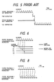
- Fig. 5 illustrates how to use the above-mentioned prior technology, wherein a VST instruction works to store the vector data in the main storage, a POST instruction works to finish the execution of the instruction after the main storage reference for all preceding instructions has been finished, a WAIT instruction works to finish the execution of the instruction after the execution of the POST instruction has been finished, and a VLD instruction works to load the vector data from the main storage.
- a VST instruction works to store the vector data in the main storage
- a POST instruction works to finish the execution of the instruction after the main storage reference for all preceding instructions has been finished
- a WAIT instruction works to finish the execution of the instruction after the execution of the POST instruction has been finished
- a VLD instruction works to load the vector data from the main storage.
- FIG. 5 is a time chart illustrating the operation in which two vector processors hand the vector data over via the main storage, and wherein an instruction sequence executed by a vector processor 1 (hereinafter referred to as VP1) is given by VST POST and an instruction sequence executed by a vector processor 2 (hereinafter referred to as VP2) is given by WAIT VLD
- the load of zero-th element of vector data on the main storage executed by the VLD instruction of VP2 needs not wait for the complete completion of the execution of VST instruction of VP1 but needs simply wait for the completion of the store of zero-th element in the VST instruction of VP1. This also holds true for the elements other than the zero-th element.
- the object of the present invention is to provide a computer which enables the operation for storing the vector data and the operation for leading the vector data to be execfuted in parallel with each other when a plurality of processors handling the vector data are to hand over the vector data via a main storage yet ensuring the sequence of main storage references and eliminating undesired waiting time.
- the present invention deals with a computer (Figs. 1, 7, 9) which comprises: (a) a main storage (3); (b) means (107, 107′) for writing onto said main storage a group of data elements having sequence; (c) means (108, 108′) for reading said group of data from said main storage; and (d) means (1, 2, 203-1 (Fig. 1), 304, 305, (Fig. 2)) which is connected to said writing means and to said reading means and which ensures the sequence of main storage references between said writing means and said reading means such that, among said group of data elements, the data elements which have not yet been written by said writing means will not be read by said reading means.
- the present invention deals with a computer system constituted by a plurality of processors which share a main storage to handle vector data, wherein each processor is provided with registration means which registers that the individual elements of vector data to be stored are written onto the main storage for each of the elements of vector data to be stored, thereby to store the data, provided with synchronized store means for effecting the registration to said registration means simultaneously therewith, and is further provided with synchronized load means which, after said data is stored in said registration means, starts to load the data and erases the registration from said registration means.
- FIG. 1 A first embodiment will now be explained in conjunction with the drawings.
- reference numeral 100 denotes a vector processor
- 200 denotes a parallel processor
- Reference numeral 1 denotes a vector semaphore register
- 3 denotes a main storage.
- the computer according to the present invention hands over the vector data between the vector processor 100 and the parallel processor 200 via main storage 3, permitting the two processors to be operated simultaneously and the vector data to be handed over at high speeds.
- reference numeral 101 denotes a vector instruction control which successively reads instructions from the main storage through a line l1 to control the execution of instructions
- 103 denotes a vector register which holds vector data of n elements from the first to n-th elements
- 102 denotes a read switch for reading vector data from the vector register 103
- reference numeral 104 denotes a write switch for writing vector data onto the vector register 103
- reference numerals 109 and 110 denotes arithmetic units that effect addition and multiplication.
- Reference numeral 105 denotes a store circuit which controls the writing of vector data from the vector register 103 onto the main storage
- 106 denotes a load circuit which controls the writing of vector data from the main storage onto the vector register 103
- reference numeral 107 denotes a synchronized store circuit that is newly provided according to the present invention
- 108 denotes a synchronized load circuit newly provided according to the present invention.
- the vector processor 100 operates as described below.
- the load circuit 106 writes some vector data from the main storage onto the vector register 103 via write switch 104.
- the arithmetic units 109 and 110 successively read the vector data from the vector register 103 via read switch 102, effect arithmetic operations such as addition and multiplication, and write the results onto the vector register 103 via write switch 104, iteratively.
- the required arithmetic operation is finished, and the result is obtained on the vector register 103.
- the store circuit 105 then writes the operated result of the vector register 103 onto the main storage via read switch 102.
- the above-mentioned operation is executed by the vector instruction control 101 in accordance with the instruction sequence successively read by the vector instruction control 101 through the line l1.
- the parallel processor 200 consists of n element processors 201-1 to 201-n, where n denotes the number of elements of vector data that can be held by the vector register 103.
- n denotes the number of elements of vector data that can be held by the vector register 103.
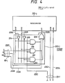
- Fig. 4 is a diagram showing the configuration of the element processor 201-j which consists of a microcomputer 202-j and a storage control 203-j.
- the microcomputer 202-j consists of a microprocessor such as Model MC6800 manufactured by Motorola Co. to which a memory is coupled. To put the present invention into practice, however, the following two instructions are newly provided.
- One of the newly provided instructions is a synchronized load instruction. Operation of the microcomputer 202-j for executing the synchronized load instruction is nearly the same as that of the general load instruction. That is, the microcomputer 202-j produces through a line l203 an address that is to be loaded, and receives the data of line l204 as a signal arrives at a line l205.
- the microcomputer 202-j In executing the synchronized load instruction, however, the microcomputer 202-j sends onto a line l201 a signal whose value is true. In other cases, the microcomputer 202-j produces onto the line l201 a signal whose truth value is false.
- Another newly provided instruction is a synchronized store instruction. Operation of the microcomputer 202-j at the time of executing the synchronized store instruction is nearly the same as that of the general store instruction. That is, the microcomputer 202-j produces from the line l203 an address that is to be stored and produces from the line l204 a data that is to be stored, and finishes the operation when a signal arrives at the line l205.
- the microcomputer 202-j At the time of executing the synchronized store instruction, however, the microcomputer 202-j produces on a line l200 a signal whose truth value is true. In other cases, the microcomputer 202-j produces on the line l200 a signal whose truth value is false.
- a storage control 203-j is newly provided for putting the present invention into practice.
- the storage control 203-j performs a particular operation which will be described later in detail.
- the storage control 203-j transmits the signal of line l202 directly to the line l205.
- the vector semaphore register 1 will now be described in conjunction with Fig. 1.
- the vector semaphore register 1 is divided into n fields each of which being imparted with first to n-th numbers and connected to element processors 201-1 to 201-n via lines l8-1 to l-8-n. Each field holds data of one bit.
- the synchronized store circuit 107 and the synchronized load circuit 108 in the vector processor 100 give access to the vector semaphore register 1.
- the switch circuit 2 is used in this case.
- the synchronized store circuit 107 writes a value 1 to each of the fields of the vector semaphore register 1 via line l4 and switch circuit 2.
- the synchronized store circuit 107 transmits to the switch circuit 2 the number of field of the vector semaphore register 1 onto which be written a value 1 over the line l4.
- the switch circuit 2 writes a value 1 onto the field of the vector semaphore register 1 designated by the synchronized store circuit 107 over the line l4.
- the synchronized load circuit 108 reads values of fields of the vector semaphore register 1 and writes value 0 thereon.
- the synchronized load circuit 108 transmits to the switch circuit 2 the number of field of the vector semaphore register 1 from which the value is to be read over line l6 or on which the value 0 is to be written as well as the instruction of which the operation is to be executed. Then, the switch circuit 2 reads via the lines l7 the value of a field of the vector semaphore register 1 designated by the synchronized load circuit 108 over the line l6 or writes the value 0 thereon.
- the synchronized store circuit 107 controls the writing of vector data from the vector register 103 onto the main storage.
- the synchronized store circuit 107 is different from the store circuit 105 in regard to that the content of the vector semaphore register 1 is changed. Fig.
- reference numeral 300 denotes a selector
- 301 denotes a register for storing an address that requests writing to the main storage
- 302 denotes a register for holding the increment of address
- 303 denotes a register for holding a value obtained by adding 1 to the number of elements of vector data to be stored in the main storage
- reference numeral 304 denotes a counter which holds the number of the element that is to be stored in the next time among all elements of vector data that are to be stored in the main storage, and sets the content thereof to an initial value 1 upon instruction from the line l2.
- the counter 304 Upon receipt of a signal "1" from the line l106, the counter 304 increases the content by 1.
- Reference 305 denotes an AND circuit for finding a logical product
- 306 denotes an adder
- Reference numeral 307 denotes a comparator which compares an input value a from a port to which the line l104 is connected with an input value b from a port to which the line l105 is connected, and which produces a signal "1" onto the line l103 only when the input values a and b are equal to each other and produces a signal "0” in other cases.
- the comparator 307 further produces a signal "1” onto the line l107 only when the input value a is greater than the input value b, and produces a signal "0" in other cases.
- the synchronized store circuit 107 operates as described below.
- the vector instruction control 101 (Fig. 1) writes onto the register 301 a main storage address for storing a first element of vector data to be stored, via line l2, selector 300 and line l100.
- the vector instruction control 101 further writes onto the register 302 via line l2 the difference of main storage addresses for storing two neighboring elements of vector data to be stored and writes onto the register 303 a value obtained by adding 1 to the number of elements of vector data to be stored.
- the vector instruction control 101 sets the content of the counter 304 to 1 via line l2 and drives the synchronized store circuit 107.
- the comparator 307 compares the value of the register 303 with the content of the counter 304. Further, a signal “0" is produced onto the line l107 and the AND circuit 305 produces a signal "0". Therefore, the content of the counter 304 remains unchanged.
- the synchronized store circuit 107 sends to the main storage 3 (Fig. 1) the content of the register 301 as a main storage address for storing the elements of vector data to be stored, via lines l101 and l12, and sends to the main storage 3 the element of vector data to be stored sent via read switch 102 in the vector processor 100 (Fig. 1) and line l3 (Fig.
- the synchronized load circuit 108 controls the writing of vector data from the main storage onto the vector register 103.
- the synchronized load circuit 108 is distinctly different from the store circuit 107 with respect to using the content of the vector semaphore register 1 for controlling the writing of vector data.
- Fig. 3 illustrates the configuration of the synchronized load circuit 108 which is nearly the same as the configuration of the synchronized store circuit 107 shown in Fig. 2, except the following two points.
- the direction of line l5 of Fig. 3 that corresponds to the line l3 of Fig. 2 is opposite to that of Fig. 2.
- This is a data line over which the synchronized load circuit 108 transfers the data from the main storage to the vector register 103.
- Another point is that a "1" judge circuit 358 is newly provided.
- the synchronized load circuit 108 operates as described below.
- the vector instruction control 101 (Fig. 1) initializes the registers 351, 352, 353 and counter 354. The manner of initialization is the same as that of the case of the synchronized store circuit 107. After initiali zation, the vector instruction control 101 drives the synchronized load circuit 108.
- the comparator 357 compares the value of the register 353 with the content of the counter 354. When the value of the register 353 is greater than the content of the counter 354, the synchronized load circuit 108 sends to the vector semaphore register 1 the content of the counter 354 via switch circuit 2 as a field number of the vector semaphore register 1 from where the value is to be read via line l6.
- the switch circuit 2 reads the signal in the field of this number in the semaphore register 1 and sends it to the "1" judge circuit 358 via line l158.
- the operation is repeated to read the above signal of the vector semaphore register 1.
- the synchronized load circuit 108 does not read the element from the main storage until the writing is finished.
- the synchronized load circuit 108 opens the AND gate 359 utilizing the output 358A of the judge circuit 358, and sends a request of read to the main storage 3 using the address in the register 351 as a main storage address for storing elements of vector data to be loaded via lines l151 and l14. After this request, the content of the register 351 and the content of the register 352 are added up together through an adder 356, and the added result is written onto the register 351 via selector 350 and line l150.
- the AND circuit 355 produces a true value onto the line l156 upon receipt, via line l15, of a signal that indicates that the main storage 3 has produced the required data onto the line l5. Then, the content of the counter 354 and the signal of the line l156 are transmitted, via line l6 and switch circuit 2, to the vector semaphore register 1 as a field number and a write request signal of vector semaphore register 1 on which the value 0 is to be written. The switch circuit 2 is reset to 0 on the field of the above number of the semaphore register 1. The output of the AND circuit 355 is transmitted to the counter 354 over a line l156, and the content of the counter 354 increases by 1.
- the corresponding fields in the semaphore register 1 are reset in synchronism with the successive loading of vector elements by the synchronized load circuit 108.
- the comparator 357 compares the two input values a and b. When the two input values are equal to each other, the comparator 357 informs to the vector instruction control 101 of the completion of operation via lines l153 and l2. Further, since a value whose truth value is false has been produced onto the line l157, the AND circuit 355 produces a false value. Therefore, the value of the counter 354 remains unchanged.
- the storage control 203-j controls access to the main storage 3 when the microcomputer 202-j executes the synchronized load instructions and the synchronized store instruction (both of which have been described already).
- the lines l8-j are connected to the j-th element in the vector semaphore register 1.
- the line l8-j consist of line l207, line l208 and line l206.
- the line l207 is an input signal line for reading a value of j-th element of the vector semaphore register 1
- the line l208 produces a set signal for setting the value of j-th element of the vector semaphore register 1 to "1”
- the line l206 produces a reset signal for resetting the value of j-th element of the vector semaphore register 1 to "0”.
- the main storage 3 When the microcomputer 202-j writes the data onto the main storage 3, the main storage 3 inputs to the line l204 a signal that represents this fact at a moment when the data produced by the microcomputer 202-j is just written onto the main storage 3.
- Reference numerals 204 and 205 denote inverters that invert input signals
- reference numerals 206, 207 and 208 denote AND circuits
- 209 denote and OR circuit.
- the storage control 203-j Described below is the operation of the storage control 203-j at the time when the microcomputer 202-j executes the synchronized load instruction.
- the microcomputer 202-j sends onto the line l203 an address of main storage 3 of data that is to be loaded, and instructs the main storage 3 to read the data.
- the microcomputer 202-j further sends a signal "1" onto the line l201 and waits for until the value on the line l205 becomes "1".
- the output of the AND circuit 207 becomes "1" and the value on the line l205 becomes "1" only when the j-th field of the vector semaphore register 1 input from the line l207 is "1" and the value from the line l202 is "1".
- the microcomputer 202-j receives the data that are read out on the line l204. That is, even when the signal "1" that indicates the completion of reading of data is input onto the line l202, the data red from the main storage 3 onto the line 204 is not received by the microcomputer 202-j owing to the synchronized load instruction unless the j-th field of the vector semaphore register 1 assumes the value "1". Further, as the output of the AND circuit 207 becomes "1", the signal is sent to the vector semaphore register 1 via line l206 to reset the value of the j-th field to 0. The same also holds true for executing the synchronized load instruction in other element processors.
- the microcomputer 202-j which executes the synchronized store instruction, sends onto the line l204 the data that is to be stored, sends onto the line l203 the address of the main storage 3 that is to be stored, and requests the writing to the main storage 3.
- the microcomputer 202-j then produces an output "1" onto the line l200 and waits until the signal on the line l205 becomes "1".
- portions that can be processed in parallel consist of portions that can be efficiently executed using a vector processor since the calculation can be regularly performed like a matrix operation, and portions which can be calculated in parallel like Monte-Carlo simulation or like a deduction processing for realizing a so-called artificial intelligence but which cannot be executed with the vector processor because of their complex calculation.
- the parallel computer according to the present invention is aimed at calculating these two portions at high speeds, the former one being carried out by the vector processor 100 and the latter one being carried out by the parallel processor 200.
- the present invention is to hand the data over at high speeds via the main storage 3.
- First, described below is the operation of the case where the vector processor 100 hands the vector data over to the parallel processor 200 via the main storage 3. It is presumed here that an address is imparted to each byte in the main storage 3, the head address of the region in the main storage 3 used for handling over the vector data is address 100 and each element of the vector data has a size of four bytes.
- the data are handed over in a manner that a first element of a vector register 103 in the vector processor 100 is handed over to the element processor 202-1 in the parallel processor 200 and the second element is handed over to the element processor 202-2, such that all elements in the vector register 103 are handed one by one over to the element processors.
- the vector processor 100 is programed in advance as follows SYVST VR 2, 100, 4 where SYVST instruction is a synchronized store instruction which causes the vector instruction control 101 to set a value 100 which is a second operand to the register 301 in the synchronized store circuit 107 shown in Fig. 2, set a value 4 which is a third operand to the register 302, set an element number n of vector data possessed by the vector register 103 to the register 303, and set a value 1 to the counter 304, and drives the synchronized store circuit 107.
- the data are read out successively from the vector register and are sent to the synchronized store circuit 107.
- the program stores the element data of the second vector register starting from the first one onto the address 100, address 104, address 108, --- of the main storage 3, successively, and further sets the values of first element, second element, third element, ----- of the vector semaphore register 1 to 1.
- the element processor 202-j (j is an integer of from 1 to n) of the parallel processor 200 is programmed in advance as follows: SYLD RO, 100 + 4* (J - 1) where SYLD instruction is a synchronized load instruction of which the operation was described already.
- SYLD instruction is a synchronized load instruction of which the operation was described already.
- the data are transferred from the vector processor 100 to the parallel processor 200 via the main storage 3 as shown in a time chart of Fig. 6.
- the element processor 202-j writes onto the main storage 3 the data in the 0-th register in a group of registers (not shown), and sets the j-th field of the vector semaphore register 1 to 1.
- the vector processor 100 is programmed in advance as follows: SYVLD VR2, 100, 4 where the SYVLD instruction is a synchronized load instruction which causes the vector instruction control 101 to set a value 100 which is a second operand to the register 351 in the synchronized load circuit 108 shown in Fig. 3, set a value 4 which is the third operand to the register 352, set the element number n of the vector data possessed by the vector register to the register 353, and set a value 1 to the counter 354, and drives the synchronized load circuit 108.
- SYVLD VR2, 100, 4 where the SYVLD instruction is a synchronized load instruction which causes the vector instruction control 101 to set a value 100 which is a second operand to the register 351 in the synchronized load circuit 108 shown in Fig. 3, set a value 4 which is the third operand to the register 352, set the element number n of the vector data possessed by the vector register to the register 353, and set a value 1 to the counter 354, and drives the synchron
- the synchronized load circuit 108 reads the data in the order of address 100, address 104, address 108, --- of main storage 3, sends the data to the second vector register 103, and sets the value to 0 in the order of first field, second field, third field, --- of the vector semaphore register 1.
- the vector data are handed over between the vector procesor 100 and the parallel processor 200 via main storage 3, and the two processors are operated simultaneously such that the vector data can be handed over at high speeds.
- FIG. 7 A second embodiment will now be described in conjunction with Fig. 7 wherein the same portions as those of Fig. 1 are denoted by the same reference numerals. Further, the referecne numerals with prime (′) represent the same portions as those denoted by the same reference numerals without prime (′).
- reference numeral 2A denotes a switch circuit which is the same as the switch circuit 2 of the first embodiment.
- Reference numerals 107 and 107′ denote synchronized store circuits, and 108 and 108′ denote synchronized load circuits.
- the parallel computer according to the present invention is to further increase the speed of calculation by executing a program which can be efficiently executed using a plurality of vector processors.
- the vector processors 100 and 100′ in the parallel computer porceed the calculation independently of each other, and the program is executed by repetitively handing over the data via the main storage 3.
- the present invention is to hand the data over via main storage 3 at high speeds in executing the program.
- the vector processor 100 hands the vector data over to the vector processor 100′ via main storage 3. It is presumed here that an address is imparted to each byte in the main storage 3, the head vector of the region in the main storage 3 used for handing over the vector data is address 100 and each element of the vector data has a size of four bytes.
- the data are handed over in a manner that a first element of a first vector register 103 in the vector processor 100 is handed over to the first element of a second vector register 102 in the vector processor 100′ and the second element is handed over to the second element, such that all elements in the first vector register 103 are handed over. Further, the fields in the vector semaphore register 1 are all set to 0.
- the vector processor 100 is programmed in advance as follows: SYVST VR2, 100, 4 where SYVST instruction is a synchronized store instruction which is the same as the one described in the first embodiment. Being programmed as described above, the vector processor 100 stores the element data of the second vector register 103 starting from the first one onto the address 100, address 104, address 108, --- of the main storage 3 successively, and further sets the values of first field, second field, third field, ---- of the vector semaphore register 1 to 1.
- the vector processor 100′ is programmed in advance as follows: SYVLD VR2, 100, 4 where SYVLD instruction is a synchronized load instruction which is the same as the one mentioned in the first embodiment. Being programmed as described above, the vector processor 100′ waits for until the values become 1 in the order of first field, second field, third field, --- of the vector semaphore register 1, reads the data in the order of address 100, address 104, address 108, --- of the main storage 3, sends the data to the second vector register 103, and sets the values to 0 in the order of first field, second field, third field, --- of the vector semaphore register 1.
- the vector data are handed over between the vector processor 100 and the vector processor 100′ via main storage as described above, and the two processors are operated simultaneously as shown in Fig. 8 such that the vector data can be handed over at high speeds.
- FIG. 9 A third embodiment will now be described in conjunction with Fig. 9.
- the third embodiment is concerned with a vector processor.
- Fig. 9 the same portions as those of Fig. 1 are denoted by the same reference numerals. Further, the reference numerals with prime (′) represent the same portions as those denoted by the same reference numerals without prime (′).
- reference numeral 101A denotes a vector instruction control which is slightly modified from the vector instruction control 101 of Fig. 1, and its details will be described later.
- Reference numeral 307 denotes a switch circuit which is newly added in this embodiment and which connects the line l6 to any one of line l306, l307 or l308 and which further connects the line l6′ to any one of line l306, l307 or l308 based upon a signal sent from the vector instruction control 101A over a line l305.
- Reference numeral 306 denotes a content addressable memory which is newly added in this embodiment and which is capable of registering the data, erasing the data or retrieving the data content addressably with a row as a unit being controlled by the vector instruction control 101A over a line l309.
- the content addressable memory receives from the vector instruction control 101A the data that is to be retrieved in the first column and the data that is to be retrieved in the second column.
- the content addressable memory informs the vector instruction control 101A of the row number.
- Reference numeral 305 denotes a "1" generator which is newly added in this embodiment, and which returns the value 1 over a line l308.
- the vector instruction control 101A uses either the synchronized store circuit 107 or 107′ when the vector data held by the vector register 103 is to be written onto the main storage 3. Which one should be used is suitably determined by the vector instruction control 101A. The description here is based on the presumption that the synchronized store circuit 107 is selected. In this case, the vector instruction control 101A of this embodiment effects for the synchronized store circuit 107 the operation which is the same as the initialization and start of the synchronized store circuit effected by the vector instruction control 101 of Fig. 1 for executing the synchronized store instruction.
- the vector instruction control 101A further stores onto the first column of first line of the content addressable memory 306 the main storage address for storing the first element of vector data to be stored via line l309, and further stores onto the second column of first line a difference in the main storage addresses for storing the two neighboring elements of vector data that is to be stored.
- the operation of the synchronized store circuit 107 that is started is finished, the data registered onto the first row of the content addressable memory 306 owing to the above-mentioned operation is then erased from the content addressable memory 306.
- the vector instruction control 101A When the vector data in the main storage 3 is to be read onto the vector register 103 by the vector instruction control 101A, use is made of either the synchronized load circuit 108 or 108′. Which one should be used is suitably determined by the vector instruction control 101A. The description here is based on the presumption that the synchronized load circuit 108 is selected. In this case, the vector instruction control 101A of this embodiment effects the following operation in addition to the operation for the synchronized load circuit 108 same as the initialization and start of the synchronized load circuit effected by the vector instruction control 101 of Fig. 1 to execute the synchronized load instruction.
- a difference between a main storage address storing a first element of vector data to be loaded and a main storage address storing two neighboring elements of vector data to be loaded, is given via line l309 to the content addressable memory 306 as data of a first row and data of second row in order to effect the content addressable retrieval.
- the vector instruction control 101A instructs via line l305 the switch circuit 307 to connect the lines l6 and l306 together.
- the vector instruction control 101A instructs the switch circuit 307 to connect the lines l6 and l307 together.
- the vector instruction control 308 instructs the switch circuit 307 to connect the lines l6 and l308 together.
- the switch circuits 2A and 2B operate in the same manner as the swtich circuit 2 of Fig. 1.
- the vector instruction control 101A monitores the first row of the content addressable memory 306 when the value returned from the content addressable memory 306 is the first row, and monitores the second row of the content addressable memory when the value that is returned is the second row.
- the vector instruction control 101A instructs via line l305 the switch circuit 307 to change the line to the line l308 to be connected to line l6.
- the vector processor operates as described below.
- the vector instruction control 101A reads vector instruction from the main storage 3, and examines if constitutional elements of the vector processor necessary for executing the operation designated by the instruction are now being in opertion.
- the constitutional elements are assigned to the instruction that is read out to start the operation of instruction, i.e., the next vector instruction is read otu to repeat the operation same as the above-mentioned operation. That is, operation of the next vector instruction can be started without waiting for the completion of operation of each of the vector instructions, and constitutional elements of the vector processor can be operated by parallel.
- the vector processor waits until the constitutional elements are no more in operation.
- VST VR2, 100, 4 (Other instruction sequences) VLD VR4, 100, 4
- VST instruction is a store instruction for successively storing vector data in the vector register designated by a first operand from the address (hereinafter referred to as base address) in the main storage 3 designated by a second operand starting from the first element maintaining a distance (hereinafter referred to as increment) of address designated by a third operand.
- the VLD instruction is a load instruction which successively loads the vector data stored maintaining a distance of increment designated by the third operand from the base address designated by the second operand onto the vector register designated by the first operand.
- the above program works to temporarily store the vector data stored in the second vector register successivesively onto address 100, address 104, address 108, --- of the main storage 3 starting from the first element, and read the vector stored in the address 100, address 104, address 108, ----- of the main storage 3 onto the fourth vector register after the operation designated by other instruction sequence is carried out.
- the vector processor initiates the operation of the next instruction without confirming the completion of the operation of the present instruction, and there exists a probability that the operation of the instruction that is started later may end earlier than the operation of the instruction that is started earlier.
- the VLD instruction may work to read the elements subsequent to the tenth element of the vector data from the main storage 3 before the tenth element of the vector data is written onto the main storage 3 by the VST instruction. That is, the sequency of main storage references may become out of order.
- the conventional vector processor is provided with an instruction for ensuring the sequence of main storage references in order to "wait for the completion of all main storage referecnes by the preceding instruction".
- the sequence of main storage references is ensured by placing the instruction for ensuring the sequence of main storage references between the store instruction and the load instruction.
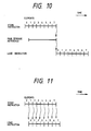
- Fig. 10 is a time chart illustrating the operation of the vector processor.
- the vector processor according to the present invention is constructed as described below.
- the store instruction is executed by using the synchronized store circuit 107 (or 107′).
- the base address and increment of a region in the main storage 3 storing the vector data are registered into the content addressable memory 306 owing to the aforementioned operation of the vector instruction control 101A, and the value 1 is successively set to the vector samaphore register 1 (or 1′) starting from the first field in the same manner as in Fig. 1.
- the load instruction is executed using the synchronized load circuit 108 (or 108′).
- the content addressable retrieval is effected for the content addressable memory 306 by the base address and increment in a region in the main storage 3 storing the vector data owing to the aforementioned operation of the vector instruction control 101A.
- the line l6 (or l6′) over which the synchronized load circuit 108 (or 108′) makes access to the vector semaphore register 1 (or 1′) is connected to the "1" generator 305 through the line l308. Therefore, the synchronized load circuit 108 (or 108′) continuously reads the vector data in the main storage 3.
- the vector instruction control 101A connects the line l6 (or l6′) to the vector semaphore register 1 or 1′ connected to the synchronized store circuit 107 or 107′ whose vector data have now been written onto the main storage 3.
- the synchronized load circuit 108 (or 108′) reads the main storage 3 while effecting the queueing so that the reading is effected after the writing for every element in the vector data. Furthermore, when the operation of the synchronized store circuit 107 or 107′ is finished while the synchronized load circuit 108 (or 108′) is reading the main storage 3 by making reference to the vector semaphore register 1 (or 1′), the vector instruction control 101A instructs the switch circuit 307 to connect the line l6 (or l6′) to the "1" generator 305. Therefore, the vector data in the main storage 3 are continuously read out by the synchronized load circuit 108 (or 108′).
- Fig. 11 is a time chart illustrating the operation of when the vector processor according to the present invention executes the above-mentioned program. It will be recognized that the operation is performed at a speed faster than that of Fig. 10.
- the vector data are handed over among a plurality of processors via the main storage. Namely, the operation of the processor for writing vector data onto the main storage on the side for sending the vector data is carried out in parallel with the operation of the processor for reading the vector data on the side for receiving the vector data yet ensuring the sequence of main storage references. Therefore, the parallel computer can be efficiently utilized.
Landscapes
- Engineering & Computer Science (AREA)
- Computer Hardware Design (AREA)
- Theoretical Computer Science (AREA)
- Computing Systems (AREA)
- Physics & Mathematics (AREA)
- General Engineering & Computer Science (AREA)
- General Physics & Mathematics (AREA)
- Complex Calculations (AREA)
Applications Claiming Priority (2)
| Application Number | Priority Date | Filing Date | Title |
|---|---|---|---|
| JP62187529A JPS6432379A (en) | 1987-07-29 | 1987-07-29 | Computer |
| JP187529/87 | 1987-07-29 |
Publications (2)
| Publication Number | Publication Date |
|---|---|
| EP0301593A2 true EP0301593A2 (fr) | 1989-02-01 |
| EP0301593A3 EP0301593A3 (fr) | 1989-11-29 |
Family
ID=16207681
Family Applications (1)
| Application Number | Title | Priority Date | Filing Date |
|---|---|---|---|
| EP88112385A Ceased EP0301593A3 (fr) | 1987-07-29 | 1988-07-29 | Calculateur pour écriture et lecture synchronisées de données vectorielles |
Country Status (3)
| Country | Link |
|---|---|
| US (1) | US4985827A (fr) |
| EP (1) | EP0301593A3 (fr) |
| JP (1) | JPS6432379A (fr) |
Families Citing this family (12)
| Publication number | Priority date | Publication date | Assignee | Title |
|---|---|---|---|---|
| JP2677414B2 (ja) * | 1989-05-15 | 1997-11-17 | 富士通株式会社 | 命令実行のシリアライズ制御方式 |
| US5265030A (en) * | 1990-04-24 | 1993-11-23 | Scripps Clinic And Research Foundation | System and method for determining three-dimensional structures of proteins |
| IE911347A1 (en) * | 1990-04-24 | 1991-11-06 | Scripps Clinic Res | System and method for determining three-dimensional¹structures of proteins |
| JPH06168263A (ja) * | 1992-11-30 | 1994-06-14 | Fujitsu Ltd | ベクトル処理装置 |
| JPH07302200A (ja) * | 1994-04-28 | 1995-11-14 | Hewlett Packard Co <Hp> | 順次付けロード動作および順序付け記憶動作を強制する命令を有するコンピュータのロード命令方法。 |
| US5699538A (en) * | 1994-12-09 | 1997-12-16 | International Business Machines Corporation | Efficient firm consistency support mechanisms in an out-of-order execution superscaler multiprocessor |
| US6117043A (en) * | 1997-11-05 | 2000-09-12 | Nsk Ltd. | Continously variable transmission having an oscillating trunnion-support yoke |
| US7320065B2 (en) | 2001-04-26 | 2008-01-15 | Eleven Engineering Incorporated | Multithread embedded processor with input/output capability |
| JP4976578B1 (ja) * | 2011-09-16 | 2012-07-18 | 楽天株式会社 | 画像検索装置およびプログラム |
| JP5577371B2 (ja) | 2012-03-29 | 2014-08-20 | 楽天株式会社 | 画像検索装置、画像検索方法およびプログラム |
| JP5577372B2 (ja) | 2012-03-29 | 2014-08-20 | 楽天株式会社 | 画像検索装置、画像検索方法、プログラムおよびコンピュータ読取り可能な記憶媒体 |
| US10521351B2 (en) * | 2017-01-12 | 2019-12-31 | International Business Machines Corporation | Temporarily suppressing processing of a restrained storage operand request |
Family Cites Families (10)
| Publication number | Priority date | Publication date | Assignee | Title |
|---|---|---|---|---|
| JPS586973B2 (ja) * | 1975-02-20 | 1983-02-07 | パナフアコム カブシキガイシヤ | メモリコテイバンチアクセスセイギヨホウシキ |
| US4128880A (en) * | 1976-06-30 | 1978-12-05 | Cray Research, Inc. | Computer vector register processing |
| US4302818A (en) * | 1979-07-10 | 1981-11-24 | Texas Instruments Incorporated | Micro-vector processor |
| US4449182A (en) * | 1981-10-05 | 1984-05-15 | Digital Equipment Corporation | Interface between a pair of processors, such as host and peripheral-controlling processors in data processing systems |
| JPS58207165A (ja) * | 1982-05-27 | 1983-12-02 | Mitsubishi Electric Corp | マルチプロセツサシステムにおけるデ−タ転送方式 |
| DE3379690D1 (en) * | 1982-09-03 | 1989-05-24 | Hitachi Ltd | Data processing system |
| US4636942A (en) * | 1983-04-25 | 1987-01-13 | Cray Research, Inc. | Computer vector multiprocessing control |
| DE3485635D1 (de) * | 1983-04-25 | 1992-05-14 | Cray Research Inc | Mehrprozessorsteuerung fuer vektorrechner. |
| JPS6224366A (ja) * | 1985-07-03 | 1987-02-02 | Hitachi Ltd | ベクトル処理装置 |
| JP2610821B2 (ja) * | 1986-01-08 | 1997-05-14 | 株式会社日立製作所 | マルチプロセツサシステム |
-
1987
- 1987-07-29 JP JP62187529A patent/JPS6432379A/ja active Pending
-
1988
- 1988-07-29 EP EP88112385A patent/EP0301593A3/fr not_active Ceased
- 1988-07-29 US US07/226,376 patent/US4985827A/en not_active Expired - Fee Related
Also Published As
| Publication number | Publication date |
|---|---|
| US4985827A (en) | 1991-01-15 |
| JPS6432379A (en) | 1989-02-02 |
| EP0301593A3 (fr) | 1989-11-29 |
Similar Documents
| Publication | Publication Date | Title |
|---|---|---|
| EP0334844B1 (fr) | Techniques de processeur virtuel dans un ensemble multiprocesseur | |
| US5093920A (en) | Programmable processing elements interconnected by a communication network including field operation unit for performing field operations | |
| US5165023A (en) | Parallel processing system with processor array and network communications system for transmitting messages of variable length | |
| US4891751A (en) | Massively parallel vector processing computer | |
| US4891787A (en) | Parallel processing system with processor array having SIMD/MIMD instruction processing | |
| US6219775B1 (en) | Massively parallel computer including auxiliary vector processor | |
| US4873626A (en) | Parallel processing system with processor array having memory system included in system memory | |
| US5418970A (en) | Parallel processing system with processor array with processing elements addressing associated memories using host supplied address value and base register content | |
| EP0301593A2 (fr) | Calculateur pour écriture et lecture synchronisées de données vectorielles | |
| US5036453A (en) | Master/slave sequencing processor | |
| EP0258736A2 (fr) | Calculateur parallèle à mémoires partagées distribuées et circuits partagés pour activer des tâches | |
| US4734882A (en) | Multilevel interrupt handling scheme | |
| JPH0766329B2 (ja) | 情報処理装置 | |
| US5678048A (en) | Interrupt vector method and apparatus for loading a slot memory address counter | |
| EP0377976B1 (fr) | Dispositif de commande microprogrammé utilisant des circuits à réseaux logiques programmables | |
| JPH0517588B2 (fr) | ||
| JP2003532224A (ja) | マルチプロセッサコンピュータシステムのための高度メモリアルゴリズミックプロセッサアーキテクチャ | |
| US4371924A (en) | Computer system apparatus for prefetching data requested by a peripheral device from memory | |
| JP3797570B2 (ja) | セマフォ命令用のセマフォ・バッファを用いた装置と方法 | |
| JP2008181551A (ja) | ベクトルレジスタを備えたコンピュータにおけるベクトルテールゲーティング | |
| US5276902A (en) | Memory access system for vector data processed or to be processed by a vector processor | |
| EP0363889A1 (fr) | Processeur vecteur avec buffer pour préparer les vecteurs de données | |
| JPH04140880A (ja) | ベクトル処理装置 | |
| JPH10260944A (ja) | 割込みシステム | |
| JPS58149555A (ja) | 並列処理装置 |
Legal Events
| Date | Code | Title | Description |
|---|---|---|---|
| PUAI | Public reference made under article 153(3) epc to a published international application that has entered the european phase |
Free format text: ORIGINAL CODE: 0009012 |
|
| AK | Designated contracting states |
Kind code of ref document: A2 Designated state(s): DE GB |
|
| PUAL | Search report despatched |
Free format text: ORIGINAL CODE: 0009013 |
|
| AK | Designated contracting states |
Kind code of ref document: A3 Designated state(s): DE GB |
|
| 17P | Request for examination filed |
Effective date: 19900529 |
|
| 17Q | First examination report despatched |
Effective date: 19940509 |
|
| STAA | Information on the status of an ep patent application or granted ep patent |
Free format text: STATUS: THE APPLICATION HAS BEEN REFUSED |
|
| 18R | Application refused |
Effective date: 19941029 |