EP0305987A2 - Selbstkorrigierendes Halbleiterspeichergerät und Mikrorechner mit einem solchen Gerät - Google Patents
Selbstkorrigierendes Halbleiterspeichergerät und Mikrorechner mit einem solchen Gerät Download PDFInfo
- Publication number
- EP0305987A2 EP0305987A2 EP88114183A EP88114183A EP0305987A2 EP 0305987 A2 EP0305987 A2 EP 0305987A2 EP 88114183 A EP88114183 A EP 88114183A EP 88114183 A EP88114183 A EP 88114183A EP 0305987 A2 EP0305987 A2 EP 0305987A2
- Authority
- EP
- European Patent Office
- Prior art keywords
- parity
- data
- read
- bit
- data bits
- Prior art date
- Legal status (The legal status is an assumption and is not a legal conclusion. Google has not performed a legal analysis and makes no representation as to the accuracy of the status listed.)
- Granted
Links
Images




Classifications
-
- G—PHYSICS
- G06—COMPUTING OR CALCULATING; COUNTING
- G06F—ELECTRIC DIGITAL DATA PROCESSING
- G06F11/00—Error detection; Error correction; Monitoring
- G06F11/07—Responding to the occurrence of a fault, e.g. fault tolerance
- G06F11/08—Error detection or correction by redundancy in data representation, e.g. by using checking codes
- G06F11/10—Adding special bits or symbols to the coded information, e.g. parity check, casting out 9's or 11's
- G06F11/1008—Adding special bits or symbols to the coded information, e.g. parity check, casting out 9's or 11's in individual solid state devices
-
- G—PHYSICS
- G06—COMPUTING OR CALCULATING; COUNTING
- G06F—ELECTRIC DIGITAL DATA PROCESSING
- G06F11/00—Error detection; Error correction; Monitoring
- G06F11/07—Responding to the occurrence of a fault, e.g. fault tolerance
- G06F11/08—Error detection or correction by redundancy in data representation, e.g. by using checking codes
- G06F11/10—Adding special bits or symbols to the coded information, e.g. parity check, casting out 9's or 11's
- G06F11/1076—Parity data used in redundant arrays of independent storages, e.g. in RAID systems
-
- G—PHYSICS
- G11—INFORMATION STORAGE
- G11C—STATIC STORES
- G11C29/00—Checking stores for correct operation ; Subsequent repair; Testing stores during standby or offline operation
- G11C29/02—Detection or location of defective auxiliary circuits, e.g. defective refresh counters
- G11C29/028—Detection or location of defective auxiliary circuits, e.g. defective refresh counters with adaption or trimming of parameters
-
- G—PHYSICS
- G11—INFORMATION STORAGE
- G11C—STATIC STORES
- G11C29/00—Checking stores for correct operation ; Subsequent repair; Testing stores during standby or offline operation
- G11C29/04—Detection or location of defective memory elements, e.g. cell constructio details, timing of test signals
- G11C29/50—Marginal testing, e.g. race, voltage or current testing
-
- G—PHYSICS
- G11—INFORMATION STORAGE
- G11C—STATIC STORES
- G11C29/00—Checking stores for correct operation ; Subsequent repair; Testing stores during standby or offline operation
- G11C29/04—Detection or location of defective memory elements, e.g. cell constructio details, timing of test signals
- G11C29/50—Marginal testing, e.g. race, voltage or current testing
- G11C29/50016—Marginal testing, e.g. race, voltage or current testing of retention
-
- G—PHYSICS
- G06—COMPUTING OR CALCULATING; COUNTING
- G06F—ELECTRIC DIGITAL DATA PROCESSING
- G06F11/00—Error detection; Error correction; Monitoring
- G06F11/07—Responding to the occurrence of a fault, e.g. fault tolerance
- G06F11/08—Error detection or correction by redundancy in data representation, e.g. by using checking codes
- G06F11/10—Adding special bits or symbols to the coded information, e.g. parity check, casting out 9's or 11's
-
- G—PHYSICS
- G06—COMPUTING OR CALCULATING; COUNTING
- G06F—ELECTRIC DIGITAL DATA PROCESSING
- G06F2201/00—Indexing scheme relating to error detection, to error correction, and to monitoring
- G06F2201/81—Threshold
-
- G—PHYSICS
- G11—INFORMATION STORAGE
- G11C—STATIC STORES
- G11C16/00—Erasable programmable read-only memories
- G11C16/02—Erasable programmable read-only memories electrically programmable
- G11C16/04—Erasable programmable read-only memories electrically programmable using variable threshold transistors, e.g. FAMOS
Definitions
- This invention relates to a nonvolatile semiconductor memory device such as an electrically erasable and programmable read-only memory (EEPROM) having the ability to correct bit errors resulting from the degradation of memory cells, and to a microcomputer incorporating such a memory device.
- EEPROM electrically erasable and programmable read-only memory
- Nonvolatile semiconductor memories are used for storing data on a permanent or semipermanent basis in a wide range of electronic devices including computers, computer peripheral equipment, office equipment, game machines, and IC cards. Although highly reliable, these nonvolatile semiconductor memories are not entirely free of bit errors caused by degradation of their constituent memory cells. In particular, EEPROM memories inevitably suffer degradation if they are reprogrammed frequently. The reliability of a nonvolatile semiconductor memory device can obviously be enhanced if the device is able to detect and correct its own bit errors.
- a similar scheme can be employed in a single-chip microcomputer comprising a central processing unit, input/output circuits, and memory on a semiconductor chip.
- the memory stores data in 2 N -bit words, with (N+1) additional parity bits for each word.
- An error-correcting-code (ECC) circuit is interposed between the memory and the data bus. When data are written in the memory, the ECC circuit generates the necessary parity bits and supplies these together with the data bits to the memory. When data are read from the memory, the ECC circuit checks the data and parity bits, detects and corrects any one-bit errors, and places the correct data on the data bus.
- ECC error-correcting-code
- An object of this invention is to provide a self-correcting semiconductor memory device that avoids the problems of low yield and high costs due to increased chip size, and a microcomputer incorporating such a self-correcting semiconductor memory device that does not require a complex error-correcting-code circuit.
- nonvolatile memory device or a microcomputer with a nonvolatile memory In a nonvolatile memory device or a microcomputer with a nonvolatile memory according to the invention, data errors arising from loss of charge in the floating gates of memory cells are detected and corrected by applying two different sense voltages to the memory cells and comparing the outputs. Instead of using a cumbersome error-correcting code, this error-correcting scheme requires only one parity bit per word, yet it can detect and correct errors in any odd number of bits. Benefits include reduced chip size and longer life for electrically erasable and programmable memories.
- Fig. 1 shows a schematic diagram of an EEPROM memory cell for storing one bit of data.
- This memory cell is described in, for example, an article on a 16K-bit EEPROM on pages 198 to 207 of Nikkei Electronics , June 23, 1980, and in Japanese Laid-open Patent Application No. 1987/32823.
- the EEPROM memory cell in Fig. 1 comprises a select transistor 1 and a memory transistor 2.
- the memory transistor 2 has a two polysilicon gate layers: a control gate 3 and a floating gate 4.
- the floating gate 4 is disposed between the control gate 3 and the channel of the memory transistor 2, and extends to a thin, localized oxide region (called a tunnel oxide) over the drain electrode.
- the data bit in the memory cell is written or erased by injecting electrons or holes into the floating gate 4 through this tunnel oxide.
- the drain electrode of the select transistor 1 is connected to a bit line 5, its gate electrode is connected to a word line 6, and its source electrode is connected to the drain electrode of the memory transistor 2.
- the control gate 3 of the memory transistor 2 is connected to a sense (or program) line 7, and its source electrode is connected to the cell ground line 8.
- the source electrode, gate electrode, and drain electrode will hereinafter be referred to simply as the source, gate, and drain.
- Table 1 indicates the voltages applied to the bit line 5, the word line 6, the sense line 7, and the cell ground line 8 when the memory cell is read, erased, and written. These operations will be described below. Table 1 Read, Erase, and Write Voltages Mode Bit line Word line Sense line Ground line Read 2V 5V 2V 0V Erase 0V 20V 20V 0V Write 20V 20V 0V Floating
- a voltage of 5V is applied to the word line 6 to turn on the select transistor 1, and voltages of, for example, 2V are applied to the bit line 5 and the sense line 7. If the voltage applied to the sense line 7 (called the sense voltage) suffices to turn on the memory transistor 2, then the bit line 5 is connected to ground (0V) and the data bit in the memory cell is read as a "0.” If the sense voltage applied to the sense line 7 does not turn on the memory transistor 2, the data bit is read as a "1.”
- the threshold voltage Vtc which must be applied to the sense line 7 to switch the memory transistor 1 on depends on the charge stored in the floating gate 4. If the floating gate 4 is already positively charged, then a small additional voltage applied to the sense line 7 will turn the memory transistor 1 on; indeed, the charge in the floating gate 4 may itself be sufficient to turn the memory transistor 1 on. In this state the memory cell stores the data "0.” If the floating gate is negatively charged, then a small voltage applied to the sense line 7 will not turn the memory transistor 1 on and the data will be read as a "1.”
- the operation of storing a negative charge in the floating gate 4 is called erasing the memory cell.
- the memory cell is erased by applying a high programming voltage (Vpp) such as 20V to the word line 6 and the sense line 7, and applying the ground level of 0V to the bit line 5 and the cell ground line 8.
- Vpp high programming voltage
- the voltage applied to the word line 6 turns on the select transistor 1, and the other voltages create a sufficient potential difference across the floating gate 4 to inject electrons from the drain into the floating gate 4 by the tunnel effect, thus raising the threshold voltage Vtc and causing the memory cell to store the data "1."
- the operation of storing a positive charge in the floating gate 4 is called writing the memory cell.
- the memory cell is written by applying the programming voltage Vpp (20V) to the bit line 5 and the word line 6, placing the sense line 7 at the ground potential of 0V, and disconnecting the cell ground line 8.
- the select transistor 1 is in the on state as in the erase operation, but now the potential difference across the floating gate 4 acts in the opposite direction to the potential difference when the cell is erased, so electrons tunnel out from the floating gate 4 to the drain and holes are injected into the floating gate 4, thus lowering the threshold voltage Vtc. In this state the memory cell stores the data "0.”
- Fig. 2 shows the Vtc characteristics when the memory cell in Fig. 1 is repeatedly reprogrammed.
- the threshold voltage Vtc is shown on the vertical axis; the number of write-erase cycles is shown on the horizontal axis.
- the changes in the threshold voltage Vtc when the cell is written and erased are plotted in relation to the number of write-erase cycles.
- the programming voltage Vpp and the write or erase time are constant.
- the line marked L1 in Fig. 2 indicates the threshold voltage Vtc when no charge is present in the floating gate 4; this threshold voltage Vtc is, for example, 1V.
- the lines marked L2 and L3 show the threshold voltage Vtc when the memory cell is erased and written, respectively.
- the tunneling of electrons and holes when the memory cell is written or erased alters the electrical properties of the tunnel oxide region.
- the cumulative effect of the alterations is to reduce the insulation breakdown voltage in the tunnel oxide region, to limit the amount of charge that can be stored in the floating gate 4, and to shorten the charge retention time.
- no degradation of the Vtc characteristic is visible over approximately the first 103 write-erase cycles, but after 104 write-erase cycles the charge injected into the floating gate by read and write operations begins to decline, and after 106 write-erase cycles the difference between Vtc in the written and erased states is considerably narrowed.
- the erase and write values of the threshold voltage after 103 write-erase cycles Vtc were 7V and -4V, respectively, they are respectively 4V and 0.5V after 106 write-erase cycles.
- the memory cell is read by a sense amplifier that detects and amplifies the current on the bit line 5 in Fig. 1.
- a large current is read as a "0;” a small current is read as a "1.”
- the current value at which the sense amplifier changes between the "0" and “1" output states is called the sense threshold current Is.
- Is The current value at which the sense amplifier changes between the "0" and “1” output states.
- the memory cell is designed so that Is is a little larger than the current It that flows when the voltage applied to the sense line 7 is exactly the threshold voltage Vtc. Accordingly, the threshold sense voltage Vs at which the output of the cell changes between "0" and “1” is a little higher than the transistor on/off threshold voltage Vtc.
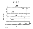
- Fig. 3 shows the characteristics of a memory cell satisfying relation (1).
- the sense threshold voltage Vs then changes from S3 (-2V for example) to S1 (3V for example), and since the sense voltage Vr is Vr1 (2V for example), the data output obtained from the sense amplifier changes from "0" to "1.”
- the sense threshold voltage Vs changes from S2 (9V for example) to S1 (3V for example). Since the sense voltage Vr is Vr1 (2V for example), the data output remains “1.”
- a partial leakage of charge from a memory cell in the erased state as in case (c) leaves the "1" data output unaltered.
- the principle of this invention is to apply a second sense voltage Vr2 differing from the first sense voltage Vr1 when the cell is read.
- Memory cells that have changed in threshold due to charge loss can be recognized by a change in the data output obtained with these differing sense voltages, and incorrect data can be corrected.
- Fig. 4 shows case (a) in Fig. 3, illustrating the principle of correction for a 1-byte (8-bit) memory cell array comprising data bits D0 to D7 and one parity bit P.
- Fig. 5 illustrates the principle of correction for case (b) in Fig. 3.
- parity bit P in Fig. 4 and Fig. 5 is set so that the 1-byte array as a whole has even parity (an even number of "1" bits.)
- Fig. 4 which corresponds to case (a) in Fig. 3, if charge escapes from the memory cell storing bit D1, when the sense voltage is Vr1, data bit D1 changes from “0" to "1,” destroying the even parity relationship. When the sense voltage is raised to Vr2, however, the data bit D1 reverts to its true value of "0.” The data from the other bits D0 and D2 to D7 remain unchanged when the sense voltage Vr2 is applied, as does the parity bit, so the even parity relationship remains true.
- the data bits D0 to D7 and parity bit P read with sense voltage Vr1 are exclusive-ORed with the data bits D0 to D7 and parity bit P read with sense voltage Vr2.
- Fig. 6 illustrates a self-correcting semiconductor memory device according to an embodiment of the present invention, based on the error-correcting principle explained above.
- the self-correcting semiconductor memory device in Fig. 6 is an EEPROM comprising a memory cell array 30.
- the memory cell array 30 comprises a plurality of nonvolatile memory cells 31 for storing data, a plurality of parity cells 32 for storing parity data, and a plurality of select transistors 33 for applying sense voltage to memory cells a byte at a time.
- Each memory cell 31 is connected to a word line 34, a bit line 35, and a sense line 37.
- Each parity cell 32 is connected to a word line 34, a parity bit line 36, and the sense line 37.
- the word lines 34 are connected to a row decoder 40.
- bit lines 35 and the parity bit lines 36 are connected through a multiplexer 42 controlled by a column decoder 41 to internal input/output (I/O) lines 43.
- the row decoder 40, the column decoder 41, and the multiplexer 42 provide a means of selecting a single memory cell 31 or a parity cell 32.
- the row decoder 40 selects a plurality of memory cells 31 in the bit line direction in the memory cell array 30; by means of a repeated column address the column decoder 41 selects a group of, for example, eight memory cells 31 and one parity cell 32 in the word line direction in the memory cell array 30; and the selected memory cells 31 and parity cell 32 are connected to the sense line 37 and to, for example, nine individual I/O lines 43.
- each I/O line 43 The function of each I/O line 43 is to transfer data to and from a memory cell 31.
- the I/O lines 43 are connected to, for example nine sense amplifiers 50 that read and amplify the data.
- the outputs of the sense amplifiers 50 are connected through nine data latch select circuits 51 to nine pairs of temporary data memory circuits comprising respectively a first latch circuit 52 and a second latch circuit 53.
- the outputs of the first latch circuit 52 and the second latch circuit 53 are connected to an exclusive-OR gate 54, the output of which is connected through an inverter 55 to the control input of the data latch select circuit 51, and also controls a sense voltage switching circuit 56 which provides a means of setting the sense voltage.
- the exclusive-OR gate 54 is a parity checking means for checking the parity of the data read by the read-out means; that is, it functions as a parity-checking circuit.
- the outputs of the first latch circuit 52 and the second latch circuit 53 are connected to an agreement checking circuit 60 which is a means of checking whether the two data values match.
- the outputs of the agreement checking circuit 60 are connected through a self-correcting circuit 70, which is a means of correcting the read-out data, to eight data output terminals 80-0 to 80-7.
- the agreement checking circuit 60 comprises eight exclusive-OR gates 60-0 to 60-7.
- the self-correcting circuit 70 comprises eight inverters 71-0 to 71-7 which receive the outputs of the exclusive-OR gates 60-0 to 60-7, and eight AND gates 72-0 to 72-7 which receive the outputs of the first latch circuits 52 and the outputs of the inverters 70-0 to 70-7.
- the outputs of the AND gates 72-0 to 72-7 are connected to the output terminals 80-0 to 80-7.
- the circuit in Fig. 6 operates as follows. Assume that in the read mode, the voltages indicated in Table 1 are applied to the selected memory cells 31 and the sense voltage on the sense line 37 has the value Vr1 illustrated in Fig. 3. Assume that the data in the memory cells 31 and parity cell 32 have been stored with even parity.
- the byte of data from the memory cells 31 is transferred through the multiplexer 42 and I/O lines 43 to the sense amplifiers 50 which detect and amplify the data, then pass the data through the data latch select circuits 51 to the first latch circuits 52 and the second latch circuits 53 in which the data values are temporarily stored.
- the exclusive-OR gate 54 checks the parity of the nine bits of read data stored in the first latch circuits 52. If the parity is even, the output of the exclusive-OR gate 54 is "0;" if the parity is odd, the output of the exclusive-OR gate 54 is "1.” If there is one defective memory cell 31 in which positive charge has escaped from the floating gate, when the sense voltage Vr1 is applied, as explained in Figs.
- the parity will be odd, so the output of the exclusive-OR gate 54 will be "1.”
- This "1" output from the exclusive-OR gate 54 is inverted by the inverter 55, causing the data latch select circuits 51 to select the second latch circuits 53, so that the sense amplifiers 50 are electrically disconnected from the first latch circuits 52 and while kept coupled to the second latch circuits 53. If the output of the exclusive-OR gate 54 were "0,” the data latch select circuits 51 would select both the first latch circuits 52 and the second latch circuits 53, and the sense amplifiers 50 would be connected to both the first latch circuits 52 and the second latch circuits 53.
- the "1" output from the exclusive-OR gate 54 also switches the sense voltage in the sense voltage switching circuit 56, increasing it from Vr1 to Vr2.
- the memory cell array 30 remains in the read mode and the same byte remains selected.
- the sense amplifiers 50 Under the sense voltage Vr2, the sense amplifiers 50 generate data output as explained in Fig. 4.
- the output of the sense amplifier 50 was a "1,” causing a violation of even parity, but when the sense voltage is increased to Vr2, the output is recognized as a "0.”
- This data value is stored in the second latch circuit 53 as the second read data.
- the outputs of the first latch circuits 52 and the second latch circuits 53 are input to the exclusive-OR gates 60-0 to 60-7 which check for agreement between the outputs of the first latch circuit 52 and the second latch circuit 53 for each bit.
- An output of "0" from the exclusive-OR gates 60-0 to 60-7 indicates agreement; an output of "1" from the exclusive-OR gates 60-0 to 60-7 indicates disagreement.
- the data do not change when read with sense voltage Vr2, so the data output from the first latch circuit 52 and the second latch circuit 53 agree.
- the data output from the first latch circuit 52 and the second latch circuit 53 disagree.
- the same data as output from the first latch circuit 52 are passed through the self-correcting circuit 70 to the data output terminals 80-0 to 80-7.
- the inverters 71-0 to 71-7 and the AND gates 72-0 to 72-7 correct the output data from the first latch circuit 52 before the data are output at the output terminals 80-0 to 80-7.
- the output of the exclusive-OR gate 54 is "0", so the voltage switch circuit does not apply the second sense voltage Vr2, and the contents of the first latch circuits 52 obtained as a result of reading with the first sense voltage Vr1 are transmitted without alteration to the terminals 80-0 to 80-7 of the self-correcting circuit 70 and used by an external circuit 110 as the correct read data.
- the second sense voltage Vr2 is applied only when a parity error is detected upon application of the first sense voltage Vr1.
- the external circuit 110 connected to the terminals 80-0 to 80-7 also receives the signal output from the exclusive-OR gate 54, according to which it recognizes as correct read data the outputs on the terminals 80-0 to 80-7 upon application of the first sense voltage Vr1 (after the first read data have been latched by the first and second latch circuits 52 and 53 and the effects of the latched first read data are transmitted to the terminals 80-0 to 80-7) if no parity error is detected upon application of the first sense voltage Vr1, and recognizes as correct read data the data on the terminals 80-0 to 80-7 upon application of the second sense voltage Vr2 if a parity error is detected and the second sense voltage Vr2 is applied.
- the first sense voltage Vr1 for the second time if no parity error is detected upon the first application of the first sense voltage Vr1.
- the same read data will again be entered in the latch circuits 52 and 53 upon the second application of the first sense voltage Vr1 the data in the first latch circuits 52 will be passed through the self-correcting circuit 70 without alteration.
- This scheme has an advantage in that the timing at which the correct data are obtained at the terminals 80-0 to 80-7 is fixed, i.e. it is always upon the second application of the sense voltage, and the sequence of operation is identical irrespective of whether or not there is an error in the read data.
- the second embodiment is similar to the first embodiment in Fig. 6 except that the data latch select circuits 51 and the sense voltage switching circuit 56 in Fig. 6 are eliminated and the output of the exclusive-OR gate 54 is supplied to the self-correcting circuit 70, which comprises AND gates 73-0 to 73-7 and exclusive-OR gates 74-1 to 74-7.
- a first sense voltage Vr1 and a second sense voltage Vr2 are applied in sequence to the gate electrodes of the memory cells 31 and parity cell 32 selected by the row decoder 40 and the column decoder 41 to obtain two sets of read data, denoted the first read data and second read data, from the sense amplifiers 50.
- the timing of the application of the first sense voltage Vr1 and the second sense voltage Vr2 is controlled by a control circuit 45, which is also connected to the clock input terminals of the first latch circuits 52 and the second latch circuits 53 and controls these latch circuits 52 and 53 so that the first latch circuits 52 latch data output when the first sense voltage Vr1 is applied and the second latch circuits 53 latch the data output when the second sense voltage Vr2 is applied.
- the exclusive-OR circuit 54 checks the parity of the first read data, and the agreement checking circuit 60 checks for agreement between the first and second read data.
- the output of the exclusive-OR gate 54 is stored in a latch circuit 75 and supplied to the AND gates 73-0 to 73-7, which also receive the outputs of the exclusive-OR gates 60-0 to 60-7, respectively.
- the outputs of the AND gates 73-0 to 73-7 are "1" when the first and second read data disagree and there is a parity error in the first read data. In all other cases the outputs of the AND gates 73-0 to 73-7 are "0.”
- An output of "1" from one of the AND gates 73-0 to 73-7 is "1" thus indicates that the corresponding memory cell is defective and the first read data is incorrect.
- the first and the second sense voltages Vr1 and Vr2 are applied in turn irrespective of whether a parity error is detected as a result of the application of the first sense voltage.
- the external circuit 110 connected to the output terminals 80-0 to 80-7 is arranged to recognize, as the correct read data, the data on the terminals 80-0 to 80-7 upon application of the second sense voltage Vr2.
- the second embodiment of this invention provides the same advantages as the first embodiment, with the additional advantage of a simpler circuit configuration, due to the elimination of the sense voltage switching circuit 56 and the data latch select circuits 51 which operated in the first embodiment depending on the parity of the data.
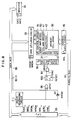
- Fig. 8 is a block diagram of the memory section of a microcomputer with a self-correcting semiconductor memory according to a third embodiment of this invention. Elements that are the same as in Fig. 6 are numbered with the same reference numerals.
- Precise error correction is possible by executing an error-correcting procedure comprising the following steps (1) to (3), which are based on principles (a) to (c) above.
- the microcomputer comprises a central processing unit CPU 89, a memory unit for storing data, and other units such as input/output units not shown in the drawing.
- the memory unit comprises a memory cell array 30 and auxiliary circuits to be described later.
- Read and write data are transferred between the memory unit and the CPU 89 via a data bus 90-1, while the memory address of the data to be written or read is sent from the CPU 89 to the memory unit via an address bus 91.
- the reading and writing of memory data are controlled by control signals such as those labeled EACC (Enable Access), WACC (Write Access), EROM (Enable ROM), WROM (Write ROM), WAL (Write Address Latch), WPEF (Write Parity Error Flag), and SYNC (Synchronize) which are output from the CPU 89 in synchronization with the system clock CLK.
- a register 92 and a data input/output latch 93 are connected to the data bus 90-1.
- the data input/output latch 93 is connected via a data/parity bus 90-2 to an input/output control circuit 94, which is connected via the sense amplifier 50, row decoder 40, column decoder 41, and multiplexer 42 to the memory cell array 30.
- the parity cells in the memory cell array 30 are connected via the sense line 37 to the sense voltage switching circuit 56.
- the row decoder 40 and column decoder 41 are connected through an address latch circuit 95 to the address bus 91.
- the memory cell array 30 is organized into a plurality of word units each consisting of, for example, eight data memory cells and one parity cell.
- the register 92 which comprises a device such as an accumulator, is for temporary storage of data to be written in the memory cell array 30, and of data read from the memory cell array 30, and has an Output Enable (OE) and a Latch (LT) terminal.
- OE Output Enable
- LT Latch
- OE Output Enable
- LT Latch
- the data input/output latch 93 has similar OE and LT terminals.
- the data input-output latch 93 When the data input-output latch 93 receives an EROM control signal at its OE terminal, it places the data read from the memory cell array 30 on the data bus 90-1. When the data input/output latch 93 receives a WROM signal at its LT terminal, it latches the data on the data bus 90-1. There is also an input/output control circuit 94 that controls the operations of writing data to the memory cell array 30 and reading data from the memory cell array 30 according to control signals received from the CPU 89. The address latch circuit 95 latches the address on the address bus 91 when it receives a WAL control signal at its LT terminal.
- the row decoder 40, the column decoder 41, and the multiplexer 42 form a means of selecting memory and parity cells in the memory cell array 30.
- the sense voltage switching circuit 56 applies the first and second sense voltages Vr1 and Vr2 to the parity cell and, together with the sense amplifier 50 and the data input/output latch 93, forms the means of reading the data.
- a parity generating circuit 96 is connected to the data bus 90-1.
- the parity generating circuit 96 is connected through a tri-state buffer 97 and a 1-bit parity bit line 98 to the data input/output latch 93.
- the parity generating circuit 96 and the parity bit line 98 are connected to an exclusive-OR gate 99 for parity checking.
- the exclusive-OR gate 99 is connected through a latch circuit 100 and an AND gate 101 to the sense voltage switching circuit 56.
- the parity generating circuit 96 which comprises a plurality of components such as exclusive-OR gates, functions as a parity generating means for generating a parity bit to satisfy, for example, an even parity condition when combined with the data on the data bus 90-1. It is possible for the parity generating means to be implemented by a program running on the CPU 89.
- the tri-state buffer 97 sends the parity bit output from the parity generating circuit 96 on the parity bit line 98.
- the tri-state buffer 97 is in the three-state (high-impedance state).
- the latch circuit 100 latches the output of the exclusive-OR gate 99 when it receives the WPEF control signal at its LT terminal, and resets when it receives the RESET control signal at its R terminals.
- the Q output terminal of the latch circuit 100 is connected to the AND gate 101.
- the Q output is used as a parity error flag to notify the CPU 89 of a parity error so that the CPU 89 can, for example, halt other operations.
- the AND gate 101 synchronizes the Q output with the synchronization signal SYNC to form a READ signal which it supplies to the sense voltage switching circuit 56.
- the sense voltage switching circuit 56 When the READ signal is active (High), the sense voltage switching circuit 56 generates the second sense voltage Vr2. When the READ signal is inactive (Low), the sense voltage switching circuit 56 generates the first sense voltage Vr1.
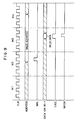
- Fig. 9 is a timing chart showing how data are written in the memory unit in Fig. 8.
- Fig. 10 is a timing chart showing how data are read from the memory unit in Fig. 8.
- the timing in Fig. 9 and Fig. 10 is synchronized with the microcomputer's system clock CLK and shows one instruction cycle (the time taken by the CPU 89 to execute one instruction) consisting of four machine cycles M1 to M4.
- the address bus and data bus are shaded in the drawing during intervals when they do not carry valid data.
- the operation of writing data stored in the register 92 into the memory cell array 30 comprises the following steps (i) to (iii).
- the operation of reading data from the memory cell array 30 and storing the data in the register 92 comprises the following steps (i) to (vii).
Landscapes
- Engineering & Computer Science (AREA)
- Theoretical Computer Science (AREA)
- Quality & Reliability (AREA)
- Physics & Mathematics (AREA)
- General Engineering & Computer Science (AREA)
- General Physics & Mathematics (AREA)
- Read Only Memory (AREA)
- Techniques For Improving Reliability Of Storages (AREA)
- For Increasing The Reliability Of Semiconductor Memories (AREA)
Applications Claiming Priority (4)
| Application Number | Priority Date | Filing Date | Title |
|---|---|---|---|
| JP217544/87 | 1987-08-31 | ||
| JP21754487 | 1987-08-31 | ||
| JP63141401A JP2509297B2 (ja) | 1987-08-31 | 1988-06-08 | 自己訂正機能付半導体記憶装置及びマイクロコンピュ―タ |
| JP141401/88 | 1988-06-08 |
Publications (3)
| Publication Number | Publication Date |
|---|---|
| EP0305987A2 true EP0305987A2 (de) | 1989-03-08 |
| EP0305987A3 EP0305987A3 (en) | 1990-08-01 |
| EP0305987B1 EP0305987B1 (de) | 1993-01-13 |
Family
ID=26473647
Family Applications (1)
| Application Number | Title | Priority Date | Filing Date |
|---|---|---|---|
| EP88114183A Expired - Lifetime EP0305987B1 (de) | 1987-08-31 | 1988-08-31 | Selbstkorrigierendes Halbleiterspeichergerät und Mikrorechner mit einem solchen Gerät |
Country Status (4)
| Country | Link |
|---|---|
| US (1) | US4901320A (de) |
| EP (1) | EP0305987B1 (de) |
| JP (1) | JP2509297B2 (de) |
| DE (1) | DE3877467T2 (de) |
Cited By (12)
| Publication number | Priority date | Publication date | Assignee | Title |
|---|---|---|---|---|
| EP0399258A3 (de) * | 1989-05-25 | 1992-01-02 | Rohm Co., Ltd. | Halbleiterspeicheranordnung mit selbstkorrigierender Funktion |
| EP0428396A3 (en) * | 1989-11-16 | 1992-04-15 | Oki Electric Industry Co., Ltd. | Bit error correcting circuit for a nonvolatile memory |
| WO1992019046A1 (en) * | 1991-04-15 | 1992-10-29 | Motorola Gmbh | EEPROM MEMORY SYSTEMS FOR 'n OUT OF m' CODES |
| WO1997041512A1 (de) * | 1996-04-25 | 1997-11-06 | Siemens Aktiengesellschaft | Verfahren zur fehlerkorrektur von datenbits in halbleiterspeichern und halbleiterspeicherchip zur durchführung des verfahrens |
| WO1999031585A1 (de) * | 1997-12-12 | 1999-06-24 | Infineon Technologies Ag | Überwachungssystem für eine digitale trimzelle |
| EP1109321A1 (de) * | 1999-12-15 | 2001-06-20 | STMicroelectronics | Einzelbit- Korrekturverfahren in einer Bitkette |
| FR2802697A1 (fr) * | 1999-12-15 | 2001-06-22 | St Microelectronics Sa | Procede de lecture d'une cellule memoire non volatile |
| EP1830269A1 (de) * | 2006-03-02 | 2007-09-05 | STMicroelectronics S.r.l. | Leseverfahren eines Speichers mit eingebetteter Fehlerkorrekturkode und Speicher mit eingebetteter Fehlerkorrekturkode |
| WO2014144043A1 (en) * | 2013-03-15 | 2014-09-18 | Marvell World Trade Ltd. | Apparatus and method for generating descriptors to reaccess a non-volatile semiconductor memory of a storage drive due to an error |
| US9135168B2 (en) | 2010-07-07 | 2015-09-15 | Marvell World Trade Ltd. | Apparatus and method for generating descriptors to reaccess a non-volatile semiconductor memory of a storage drive due to an error |
| US9141538B2 (en) | 2010-07-07 | 2015-09-22 | Marvell World Trade Ltd. | Apparatus and method for generating descriptors to transfer data to and from non-volatile semiconductor memory of a storage drive |
| US9183141B2 (en) | 2010-07-07 | 2015-11-10 | Marvell World Trade Ltd. | Method and apparatus for parallel transfer of blocks of data between an interface module and a non-volatile semiconductor memory |
Families Citing this family (29)
| Publication number | Priority date | Publication date | Assignee | Title |
|---|---|---|---|---|
| DE69024086T2 (de) * | 1989-04-13 | 1996-06-20 | Sundisk Corp | EEprom-System mit Blocklöschung |
| US5134616A (en) * | 1990-02-13 | 1992-07-28 | International Business Machines Corporation | Dynamic ram with on-chip ecc and optimized bit and word redundancy |
| JPH04141900A (ja) * | 1990-10-01 | 1992-05-15 | Nec Ic Microcomput Syst Ltd | 半導体集積回路 |
| JP3171599B2 (ja) * | 1991-03-05 | 2001-05-28 | 沖電気工業株式会社 | 半導体記憶装置 |
| US5504760A (en) * | 1991-03-15 | 1996-04-02 | Sandisk Corporation | Mixed data encoding EEPROM system |
| US5450354A (en) * | 1992-08-31 | 1995-09-12 | Nippon Steel Corporation | Non-volatile semiconductor memory device detachable deterioration of memory cells |
| US5883903A (en) * | 1993-09-20 | 1999-03-16 | Fujitsu Limited | Semiconductor memory of XN type having parity corresponding to n×m bits |
| US5872802A (en) * | 1996-05-03 | 1999-02-16 | Cypress Semiconductor Corp. | Parity generation and check circuit and method in read data path |
| JP3215344B2 (ja) * | 1997-03-10 | 2001-10-02 | 株式会社東芝 | プロセッサ及びそのバグ回避方法 |
| DE19916065A1 (de) | 1999-04-09 | 2000-10-19 | Siemens Ag | Programmierbarer Festwertspeicher und Verfahren zum Betreiben des Festwertspeichers |
| JP4316085B2 (ja) * | 1999-12-28 | 2009-08-19 | 株式会社東芝 | 半導体集積回路装置及び集積回路システム |
| JP2002074999A (ja) * | 2000-08-23 | 2002-03-15 | Sharp Corp | 不揮発性半導体記憶装置 |
| US7301961B1 (en) | 2001-12-27 | 2007-11-27 | Cypress Semiconductor Corportion | Method and apparatus for configuring signal lines according to idle codes |
| CA2447204C (en) * | 2002-11-29 | 2010-03-23 | Memory Management Services Ltd. | Error correction scheme for memory |
| US7615039B2 (en) * | 2004-09-16 | 2009-11-10 | Mcneil-Ppc, Inc. | Body attachable drapeable sanitary absorbent napkin |
| JP4178248B2 (ja) * | 2004-10-28 | 2008-11-12 | 富士通マイクロエレクトロニクス株式会社 | 半導体装置 |
| JP2009505188A (ja) * | 2005-08-11 | 2009-02-05 | コンティネンタル・テーベス・アクチエンゲゼルシヤフト・ウント・コンパニー・オッフェネ・ハンデルスゲゼルシヤフト | 少なくとも部分的に安全上重大なプロセスの制御または調節用マイクロプロセッサシステム |
| JP4991131B2 (ja) * | 2005-08-12 | 2012-08-01 | 株式会社東芝 | 半導体記憶装置 |
| JP4660353B2 (ja) * | 2005-11-01 | 2011-03-30 | 株式会社東芝 | 記憶媒体再生装置 |
| US7423912B2 (en) * | 2006-09-19 | 2008-09-09 | Atmel Corporation | SONOS memory array with improved read disturb characteristic |
| JP5422976B2 (ja) | 2008-11-19 | 2014-02-19 | 富士通株式会社 | 半導体記憶装置 |
| JP2010055746A (ja) * | 2009-12-07 | 2010-03-11 | Toshiba Corp | 記憶媒体再生装置、記憶媒体再生方法および記憶媒体再生プログラム |
| CN104220991B (zh) * | 2012-03-16 | 2017-08-29 | 马维尔国际贸易有限公司 | 用于允许数据在nand闪存上的有效存储的架构 |
| US20140201599A1 (en) * | 2013-01-15 | 2014-07-17 | International Business Machines Corporation | Error protection for integrated circuits in an insensitive direction |
| US9021328B2 (en) | 2013-01-15 | 2015-04-28 | International Business Machines Corporation | Shared error protection for register banks |
| US9201727B2 (en) | 2013-01-15 | 2015-12-01 | International Business Machines Corporation | Error protection for a data bus |
| US9041428B2 (en) | 2013-01-15 | 2015-05-26 | International Business Machines Corporation | Placement of storage cells on an integrated circuit |
| US9043683B2 (en) | 2013-01-23 | 2015-05-26 | International Business Machines Corporation | Error protection for integrated circuits |
| US20210191638A1 (en) * | 2017-09-15 | 2021-06-24 | Pure Storage, Inc. | Voltage thresholds in flash devices |
Family Cites Families (6)
| Publication number | Priority date | Publication date | Assignee | Title |
|---|---|---|---|---|
| GB1193287A (en) * | 1967-08-08 | 1970-05-28 | Ferranti Ltd | Improvements relating to Apparatus for Reading Magnetic Tape |
| US3582880A (en) * | 1969-12-05 | 1971-06-01 | Ibm | Data error correction by inversion storage |
| DE2758390B2 (de) * | 1977-12-28 | 1979-10-25 | Siemens Ag, 1000 Berlin Und 8000 Muenchen | Fehlerprüf schaltung |
| US4360915A (en) * | 1979-02-07 | 1982-11-23 | The Warner & Swasey Company | Error detection means |
| JPS6035760B2 (ja) * | 1980-12-18 | 1985-08-16 | 富士通株式会社 | 半導体記憶装置 |
| DE3205473A1 (de) * | 1982-02-16 | 1983-08-25 | Siemens AG, 1000 Berlin und 8000 München | Verfahren und anordnung zur funktionspruefung eines elektrisch wortweise umprogrammierbaren speichers |
-
1988
- 1988-06-08 JP JP63141401A patent/JP2509297B2/ja not_active Expired - Fee Related
- 1988-08-31 DE DE8888114183T patent/DE3877467T2/de not_active Expired - Fee Related
- 1988-08-31 EP EP88114183A patent/EP0305987B1/de not_active Expired - Lifetime
- 1988-08-31 US US07/238,811 patent/US4901320A/en not_active Expired - Lifetime
Cited By (17)
| Publication number | Priority date | Publication date | Assignee | Title |
|---|---|---|---|---|
| EP0399258A3 (de) * | 1989-05-25 | 1992-01-02 | Rohm Co., Ltd. | Halbleiterspeicheranordnung mit selbstkorrigierender Funktion |
| EP0428396A3 (en) * | 1989-11-16 | 1992-04-15 | Oki Electric Industry Co., Ltd. | Bit error correcting circuit for a nonvolatile memory |
| US5206866A (en) * | 1989-11-16 | 1993-04-27 | Oki Electric Industry Co., Ltd. | Bit error correcting circuit for a nonvolatile memory |
| WO1992019046A1 (en) * | 1991-04-15 | 1992-10-29 | Motorola Gmbh | EEPROM MEMORY SYSTEMS FOR 'n OUT OF m' CODES |
| WO1997041512A1 (de) * | 1996-04-25 | 1997-11-06 | Siemens Aktiengesellschaft | Verfahren zur fehlerkorrektur von datenbits in halbleiterspeichern und halbleiterspeicherchip zur durchführung des verfahrens |
| WO1999031585A1 (de) * | 1997-12-12 | 1999-06-24 | Infineon Technologies Ag | Überwachungssystem für eine digitale trimzelle |
| FR2802697A1 (fr) * | 1999-12-15 | 2001-06-22 | St Microelectronics Sa | Procede de lecture d'une cellule memoire non volatile |
| FR2802734A1 (fr) * | 1999-12-15 | 2001-06-22 | St Microelectronics Sa | Procede de correction d'un bit dans une chaine de bits |
| EP1109321A1 (de) * | 1999-12-15 | 2001-06-20 | STMicroelectronics | Einzelbit- Korrekturverfahren in einer Bitkette |
| US6735733B2 (en) | 1999-12-15 | 2004-05-11 | Stmicroelectronics Sa | Method for the correction of a bit in a string of bits |
| EP1830269A1 (de) * | 2006-03-02 | 2007-09-05 | STMicroelectronics S.r.l. | Leseverfahren eines Speichers mit eingebetteter Fehlerkorrekturkode und Speicher mit eingebetteter Fehlerkorrekturkode |
| US7908543B2 (en) | 2006-03-02 | 2011-03-15 | Alessia Marelli | Reading method of a memory device with embedded error-correcting code and memory device with embedded error-correcting code |
| US8347201B2 (en) | 2006-03-02 | 2013-01-01 | Micron Technology, Inc. | Reading method of a memory device with embedded error-correcting code and memory device with embedded error-correcting code |
| US9135168B2 (en) | 2010-07-07 | 2015-09-15 | Marvell World Trade Ltd. | Apparatus and method for generating descriptors to reaccess a non-volatile semiconductor memory of a storage drive due to an error |
| US9141538B2 (en) | 2010-07-07 | 2015-09-22 | Marvell World Trade Ltd. | Apparatus and method for generating descriptors to transfer data to and from non-volatile semiconductor memory of a storage drive |
| US9183141B2 (en) | 2010-07-07 | 2015-11-10 | Marvell World Trade Ltd. | Method and apparatus for parallel transfer of blocks of data between an interface module and a non-volatile semiconductor memory |
| WO2014144043A1 (en) * | 2013-03-15 | 2014-09-18 | Marvell World Trade Ltd. | Apparatus and method for generating descriptors to reaccess a non-volatile semiconductor memory of a storage drive due to an error |
Also Published As
| Publication number | Publication date |
|---|---|
| DE3877467T2 (de) | 1993-08-12 |
| EP0305987A3 (en) | 1990-08-01 |
| DE3877467D1 (de) | 1993-02-25 |
| JPH01133300A (ja) | 1989-05-25 |
| US4901320A (en) | 1990-02-13 |
| JP2509297B2 (ja) | 1996-06-19 |
| EP0305987B1 (de) | 1993-01-13 |
Similar Documents
| Publication | Publication Date | Title |
|---|---|---|
| EP0305987B1 (de) | Selbstkorrigierendes Halbleiterspeichergerät und Mikrorechner mit einem solchen Gerät | |
| EP0307958B1 (de) | EEPROM-System mit Bitfehlererkennungsfunktion | |
| US6216251B1 (en) | On-chip error detection and correction system for an embedded non-volatile memory array and method of operation | |
| JP4105819B2 (ja) | 記憶装置およびメモリカード | |
| JP4034949B2 (ja) | 不揮発性半導体記憶装置 | |
| US8943387B2 (en) | Programming management data for a memory | |
| US5128944A (en) | Apparatus and method for providing notification of bit-cell failure in a redundant-bit-cell memory | |
| US8954818B2 (en) | Error detection and correction scheme for a memory device | |
| US8139412B2 (en) | Systematic error correction for multi-level flash memory | |
| US4958352A (en) | Semiconductor memory device with error check and correcting function | |
| US5151906A (en) | Semiconductor memory device having self-correcting function | |
| US5448578A (en) | Electrically erasable and programmable read only memory with an error check and correction circuit | |
| US6108236A (en) | Smart card comprising integrated circuitry including EPROM and error check and correction system | |
| US20080034253A1 (en) | Ferroelectric memory with spare memory cell array and ecc circuit | |
| US6847554B2 (en) | Nonvolatile semiconductor memory device with error detection and correction circuit | |
| US6131177A (en) | System including a ferroelectric memory | |
| JPH0683716A (ja) | 電気的書換可能型不揮発メモリ | |
| EP0428396B1 (de) | Bitfehlerkorrekturschaltung für einen nichtflüchtigen Speicher | |
| JPH0831196A (ja) | 半導体メモリ | |
| HK1001240A (en) | Self-correcting semiconductor memory device and microcomputer incorporating the same | |
| HK1001240B (en) | Self-correcting semiconductor memory device and microcomputer incorporating the same | |
| JP2003100095A (ja) | 半導体集積回路装置 | |
| JP2009176393A (ja) | 不揮発性半導体記憶装置及びその自動テスト方法 | |
| JP2695278B2 (ja) | 単一チップ型マイクロコンピュータ | |
| JPS6047299A (ja) | 半導体集積回路 |
Legal Events
| Date | Code | Title | Description |
|---|---|---|---|
| PUAI | Public reference made under article 153(3) epc to a published international application that has entered the european phase |
Free format text: ORIGINAL CODE: 0009012 |
|
| AK | Designated contracting states |
Kind code of ref document: A2 Designated state(s): DE FR GB |
|
| PUAL | Search report despatched |
Free format text: ORIGINAL CODE: 0009013 |
|
| AK | Designated contracting states |
Kind code of ref document: A3 Designated state(s): DE FR GB |
|
| 17P | Request for examination filed |
Effective date: 19900910 |
|
| 17Q | First examination report despatched |
Effective date: 19920406 |
|
| GRAA | (expected) grant |
Free format text: ORIGINAL CODE: 0009210 |
|
| AK | Designated contracting states |
Kind code of ref document: B1 Designated state(s): DE FR GB |
|
| REF | Corresponds to: |
Ref document number: 3877467 Country of ref document: DE Date of ref document: 19930225 |
|
| ET | Fr: translation filed | ||
| PLBE | No opposition filed within time limit |
Free format text: ORIGINAL CODE: 0009261 |
|
| STAA | Information on the status of an ep patent application or granted ep patent |
Free format text: STATUS: NO OPPOSITION FILED WITHIN TIME LIMIT |
|
| 26N | No opposition filed | ||
| REG | Reference to a national code |
Ref country code: GB Ref legal event code: IF02 |
|
| PGFP | Annual fee paid to national office [announced via postgrant information from national office to epo] |
Ref country code: FR Payment date: 20020808 Year of fee payment: 15 |
|
| PGFP | Annual fee paid to national office [announced via postgrant information from national office to epo] |
Ref country code: GB Payment date: 20020828 Year of fee payment: 15 |
|
| PGFP | Annual fee paid to national office [announced via postgrant information from national office to epo] |
Ref country code: DE Payment date: 20020904 Year of fee payment: 15 |
|
| PG25 | Lapsed in a contracting state [announced via postgrant information from national office to epo] |
Ref country code: GB Free format text: LAPSE BECAUSE OF NON-PAYMENT OF DUE FEES Effective date: 20030831 |
|
| PG25 | Lapsed in a contracting state [announced via postgrant information from national office to epo] |
Ref country code: DE Free format text: LAPSE BECAUSE OF NON-PAYMENT OF DUE FEES Effective date: 20040302 |
|
| GBPC | Gb: european patent ceased through non-payment of renewal fee | ||
| PG25 | Lapsed in a contracting state [announced via postgrant information from national office to epo] |
Ref country code: FR Free format text: LAPSE BECAUSE OF NON-PAYMENT OF DUE FEES Effective date: 20040430 |
|
| REG | Reference to a national code |
Ref country code: FR Ref legal event code: ST |