EP0306287A2 - Supraleitende Schaltungen aus Keramik und Verfahren zu ihrer Herstellung - Google Patents
Supraleitende Schaltungen aus Keramik und Verfahren zu ihrer Herstellung Download PDFInfo
- Publication number
- EP0306287A2 EP0306287A2 EP88308048A EP88308048A EP0306287A2 EP 0306287 A2 EP0306287 A2 EP 0306287A2 EP 88308048 A EP88308048 A EP 88308048A EP 88308048 A EP88308048 A EP 88308048A EP 0306287 A2 EP0306287 A2 EP 0306287A2
- Authority
- EP
- European Patent Office
- Prior art keywords
- superconducting
- pattern
- ceramic
- patterns
- insulating
- Prior art date
- Legal status (The legal status is an assumption and is not a legal conclusion. Google has not performed a legal analysis and makes no representation as to the accuracy of the status listed.)
- Granted
Links
Images

Classifications
-
- H—ELECTRICITY
- H01—ELECTRIC ELEMENTS
- H01F—MAGNETS; INDUCTANCES; TRANSFORMERS; SELECTION OF MATERIALS FOR THEIR MAGNETIC PROPERTIES
- H01F41/00—Apparatus or processes specially adapted for manufacturing or assembling magnets, inductances or transformers; Apparatus or processes specially adapted for manufacturing materials characterised by their magnetic properties
- H01F41/02—Apparatus or processes specially adapted for manufacturing or assembling magnets, inductances or transformers; Apparatus or processes specially adapted for manufacturing materials characterised by their magnetic properties for manufacturing cores, coils, or magnets
- H01F41/04—Apparatus or processes specially adapted for manufacturing or assembling magnets, inductances or transformers; Apparatus or processes specially adapted for manufacturing materials characterised by their magnetic properties for manufacturing cores, coils, or magnets for manufacturing coils
- H01F41/048—Superconductive coils
-
- H—ELECTRICITY
- H01—ELECTRIC ELEMENTS
- H01F—MAGNETS; INDUCTANCES; TRANSFORMERS; SELECTION OF MATERIALS FOR THEIR MAGNETIC PROPERTIES
- H01F6/00—Superconducting magnets; Superconducting coils
- H01F6/06—Coils, e.g. winding, insulating, terminating or casing arrangements therefor
-
- H—ELECTRICITY
- H10—SEMICONDUCTOR DEVICES; ELECTRIC SOLID-STATE DEVICES NOT OTHERWISE PROVIDED FOR
- H10N—ELECTRIC SOLID-STATE DEVICES NOT OTHERWISE PROVIDED FOR
- H10N60/00—Superconducting devices
- H10N60/20—Permanent superconducting devices
- H10N60/203—Permanent superconducting devices comprising high-Tc ceramic materials
-
- Y—GENERAL TAGGING OF NEW TECHNOLOGICAL DEVELOPMENTS; GENERAL TAGGING OF CROSS-SECTIONAL TECHNOLOGIES SPANNING OVER SEVERAL SECTIONS OF THE IPC; TECHNICAL SUBJECTS COVERED BY FORMER USPC CROSS-REFERENCE ART COLLECTIONS [XRACs] AND DIGESTS
- Y10—TECHNICAL SUBJECTS COVERED BY FORMER USPC
- Y10S—TECHNICAL SUBJECTS COVERED BY FORMER USPC CROSS-REFERENCE ART COLLECTIONS [XRACs] AND DIGESTS
- Y10S428/00—Stock material or miscellaneous articles
- Y10S428/901—Printed circuit
-
- Y—GENERAL TAGGING OF NEW TECHNOLOGICAL DEVELOPMENTS; GENERAL TAGGING OF CROSS-SECTIONAL TECHNOLOGIES SPANNING OVER SEVERAL SECTIONS OF THE IPC; TECHNICAL SUBJECTS COVERED BY FORMER USPC CROSS-REFERENCE ART COLLECTIONS [XRACs] AND DIGESTS
- Y10—TECHNICAL SUBJECTS COVERED BY FORMER USPC
- Y10S—TECHNICAL SUBJECTS COVERED BY FORMER USPC CROSS-REFERENCE ART COLLECTIONS [XRACs] AND DIGESTS
- Y10S428/00—Stock material or miscellaneous articles
- Y10S428/922—Static electricity metal bleed-off metallic stock
- Y10S428/9265—Special properties
- Y10S428/93—Electric superconducting
-
- Y—GENERAL TAGGING OF NEW TECHNOLOGICAL DEVELOPMENTS; GENERAL TAGGING OF CROSS-SECTIONAL TECHNOLOGIES SPANNING OVER SEVERAL SECTIONS OF THE IPC; TECHNICAL SUBJECTS COVERED BY FORMER USPC CROSS-REFERENCE ART COLLECTIONS [XRACs] AND DIGESTS
- Y10—TECHNICAL SUBJECTS COVERED BY FORMER USPC
- Y10S—TECHNICAL SUBJECTS COVERED BY FORMER USPC CROSS-REFERENCE ART COLLECTIONS [XRACs] AND DIGESTS
- Y10S505/00—Superconductor technology: apparatus, material, process
- Y10S505/70—High TC, above 30 k, superconducting device, article, or structured stock
- Y10S505/701—Coated or thin film device, i.e. active or passive
- Y10S505/702—Josephson junction present
-
- Y—GENERAL TAGGING OF NEW TECHNOLOGICAL DEVELOPMENTS; GENERAL TAGGING OF CROSS-SECTIONAL TECHNOLOGIES SPANNING OVER SEVERAL SECTIONS OF THE IPC; TECHNICAL SUBJECTS COVERED BY FORMER USPC CROSS-REFERENCE ART COLLECTIONS [XRACs] AND DIGESTS
- Y10—TECHNICAL SUBJECTS COVERED BY FORMER USPC
- Y10S—TECHNICAL SUBJECTS COVERED BY FORMER USPC CROSS-REFERENCE ART COLLECTIONS [XRACs] AND DIGESTS
- Y10S505/00—Superconductor technology: apparatus, material, process
- Y10S505/70—High TC, above 30 k, superconducting device, article, or structured stock
- Y10S505/701—Coated or thin film device, i.e. active or passive
- Y10S505/703—Microelectronic device with superconducting conduction line
-
- Y—GENERAL TAGGING OF NEW TECHNOLOGICAL DEVELOPMENTS; GENERAL TAGGING OF CROSS-SECTIONAL TECHNOLOGIES SPANNING OVER SEVERAL SECTIONS OF THE IPC; TECHNICAL SUBJECTS COVERED BY FORMER USPC CROSS-REFERENCE ART COLLECTIONS [XRACs] AND DIGESTS
- Y10—TECHNICAL SUBJECTS COVERED BY FORMER USPC
- Y10S—TECHNICAL SUBJECTS COVERED BY FORMER USPC CROSS-REFERENCE ART COLLECTIONS [XRACs] AND DIGESTS
- Y10S505/00—Superconductor technology: apparatus, material, process
- Y10S505/70—High TC, above 30 k, superconducting device, article, or structured stock
- Y10S505/704—Wire, fiber, or cable
-
- Y—GENERAL TAGGING OF NEW TECHNOLOGICAL DEVELOPMENTS; GENERAL TAGGING OF CROSS-SECTIONAL TECHNOLOGIES SPANNING OVER SEVERAL SECTIONS OF THE IPC; TECHNICAL SUBJECTS COVERED BY FORMER USPC CROSS-REFERENCE ART COLLECTIONS [XRACs] AND DIGESTS
- Y10—TECHNICAL SUBJECTS COVERED BY FORMER USPC
- Y10T—TECHNICAL SUBJECTS COVERED BY FORMER US CLASSIFICATION
- Y10T428/00—Stock material or miscellaneous articles
- Y10T428/24—Structurally defined web or sheet [e.g., overall dimension, etc.]
- Y10T428/24802—Discontinuous or differential coating, impregnation or bond [e.g., artwork, printing, retouched photograph, etc.]
- Y10T428/24917—Discontinuous or differential coating, impregnation or bond [e.g., artwork, printing, retouched photograph, etc.] including metal layer
-
- Y—GENERAL TAGGING OF NEW TECHNOLOGICAL DEVELOPMENTS; GENERAL TAGGING OF CROSS-SECTIONAL TECHNOLOGIES SPANNING OVER SEVERAL SECTIONS OF THE IPC; TECHNICAL SUBJECTS COVERED BY FORMER USPC CROSS-REFERENCE ART COLLECTIONS [XRACs] AND DIGESTS
- Y10—TECHNICAL SUBJECTS COVERED BY FORMER USPC
- Y10T—TECHNICAL SUBJECTS COVERED BY FORMER US CLASSIFICATION
- Y10T428/00—Stock material or miscellaneous articles
- Y10T428/24—Structurally defined web or sheet [e.g., overall dimension, etc.]
- Y10T428/24802—Discontinuous or differential coating, impregnation or bond [e.g., artwork, printing, retouched photograph, etc.]
- Y10T428/24926—Discontinuous or differential coating, impregnation or bond [e.g., artwork, printing, retouched photograph, etc.] including ceramic, glass, porcelain or quartz layer
Definitions
- This invention relates to superconducting ceramic circuits and manufacturing methods for the same.
- an oxide mixture for constituting a superconducting ceramic is deposited in the form of a thin film on a substrate, e.g. by sputtering such as magnetron sputtering, printing such as screen press printing, spraying such as plasma spraying, electron beam evaporation or other methods.
- the deposited ceramic film is then fired at 500-1000°C, e.g. 900°C for 15 hours. After gradually cooling at a rate of 200°C/min or slower, e.g. 10°C/min, the ceramic film is further oxidized at 450°C for an hour, if necessary.
- a magnetic field may be applied to the deposited film in order to expedite the formation of crystalline structure.
- the superconducting film is irradiated and scanned with a laser beam along a prescribed pattern in order to remove the film partly.
- lasers for this use are YAG lasers (1.06 microns), eximer lasers (KrF or KrCl), argon lasers, and nitrogen lasers.
- YAG lasers can emit infrared laser pulses having a circular cross section at 5-100KHz.
- the pulse width of YAG lasers is not shorter than 50 nm, and therefore, if fine control of processing depths of laser scribing is desired, eximer lasers are suitable for this application because the pulse width is as short as 20 microns.
- excimer laser beams can be squeezed to a diameter of 10-100 microns.
- a representative pattern is spirals in the form of superconducting coils.
- the superconducting pattern on the substrate is covered with an insulating coating. It is important to make the insulating coating from a material whose thermal expansion coefficient is approximately equal to that of the superconducting pattern.
- the insulating coating is non-superconducting and preferably made of a ceramic material similar to the material forming the superconducting pattern. A portion of the insulating coating just above the end of the superconducting coil is removed to provide an opening. Then, another superconducting ceramic film is superimposed on the insulating film and patterned into an upper spiral form in order to be coupled with the lower superconducting coil through the opening. The windings of the upper and lower spirals have to be in opposite directions so that the inductances are summed rather than cancelled out.
- non-superconducting ceramics [(A′ p A ⁇ 1-p ) 1-x (B′ q B ⁇ 1-q ) x ] y (Cu r X 1-r ) z O w , where A′ is one or more elements of Group IIIa of the Priodic Table, e.g., the rare earth elements or lantanoides, B′ is one or more alkaline earth metals, i.e.
- the numbers p, q and r are chosen to be 0.99 to 0.80 so that the total proportion of A ⁇ , B ⁇ and X is 1-20 vol% in the ceramic material, particularly in case of Mg and Al, the proportion may be 1-5%.
- the non-superconducting ceramic film and the superconducting ceramic film can be formed by spraying method for example. Namely, nitrates, hidrochlorides, and/or oxalate of the elements are dissolved in water and nutralized by ammonia in order to produce extremely fine particles. These fine particles are coated on a surface, dried and fired in an oxidizing atmosphere such as an excited oxygen atmosphere. This firing process can be carried out at relatively low temperatures by making use of an O3 atmosphere.
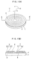
- a circular substrate 1 is made of a caramic material such as alumina, silicon oxide, alminium nitride, zirconia, yttria or YSZ(yttria stabilized zircon), or a metal or a quartz glass.
- YSZ, yttria or zirconia are particularly suitable having regard to the desirability of matching the coefficient of thermal expansion rate of the substrate to that of the superconducting film formed thereon as hereinafter described.
- the differential coefficient of thermal expansion between the underlying substrate and the overlying ceramic thin film to cover them should be as small as possible prefer strictlyably within 50% of the ceramic thin film. If the substrate and the ceramic thin film have substantially different thermal coefficients, strain developed between them may hinder the formation of superconducting structure by recrystallization of the ceramic films.
- the surface of the substrate cay be coated with a "non-superconducting ceramic" material.
- Prescribed amounts of oxides, carbonate and/or halides are mixed together in a ball mill, compacted and fired.
- the fired mixture is deposited on the substrate 1 at a substrate temperature of 650°C to a thickness of 0.1 to 50 microns, e.g. 20 microns by magnetoron sputtering using a target of the fired mixture in an oxygen atmosphere containing 20% argon.
- the deposited film is annealed at 850°C for 8 hours, gradually cooled at 4°C per minute and annealed again at 400°C for 2 hours.
- a superconducting structure of the ceramic which is sublimable is constructed with its (a,b) plane in parallel with the substrate.
- the surface of the superconducting film is scanned with irradiation of laser pulses from an eximer laser (254nm) of 50 microns diameter along a spiral path while the circular substrate is turning.
- the laser pulse location is shifted from a prepheral position toward the center of the circular substrate to form the spiral.
- the irradiated portion of the superconducting film is removed by sublimation, and a spiral groove is formed so that a superconducting spiral pattern remains.
- the peak output level of the laser pulses is 106 to 108 W/sec. This laser scribing may be performed before the annealing of the ceramic film instead.
- the superconducting spiral on the upper surface of the substate is isolated by coating an insulating film made of a "non-superconducting ceramic". It is important that the insulating film is selected to have a thermal expansion coefficient approximately equal to that of the superconducing spiral. A portion of the insulating film is eliminated to form an opening in order to expose the inner end 8 of the superconducting spiral.
- a ceramic oxide film is deposited again on the structure, fired and patterned in the same manner to be an upper superconducting spiral.
- the upper superconducting ceramic spiral turns in the reverse direction to the lower superconducting ceramic spiral. Since the upper and lower spirals are coupled through the opening, a double-layered coil is constructed with a doubled inductance.
- FIG.2(A) and 2(B) another embodiment of the present invention will be described.
- equivalent procedure of the previous embodiment is carried out but on the surface of a cylinder 11.
- Deposition is performed on the cylindrical surface coated with a "non-superconducting ceramic" film 12 with the cylinder 11 turning.
- the path of laser pulses 4 is shifted toward the right direction on the left end of the turning cylinder as indicated by arrow. Accordingly, a herical groove 13 is formed on the film leaving a first superconducting helix 15.
- a first "non-superconducting ceramic" film 17 is formed with an opening at one end 15-1 of the first helix.
- a second superconducting helix 7 and a second "non-superconducting ceramic" film 21 with an opening at one end 19-1 of the second helix 7 are formed in the same manner.
- the other end 19-2 of the second helix is coupled with the first helix 15 through the opening of the first non-super conducting film 17.
- An opening is formed penetrating through the first and second non-superconducting films 17 and 21.
- a thrid superconducting helix 23 is formed in order that it is coupled at one end 23-1 thereof with the second superconducting helix 19 through the opening.
- a triple-layered coil is formed.
- One terminal is the other end 23-2 of the third helix and the other terminal is the other end 15-2 of the first helix 2.
- the other terminal 15-2 is provided with a contact 25 making contact with the other end of the first helix through the opening at the other end 15-2.
- temporary substrates are prepared in the forms of the substrates 1 and 11 as illustrated in Figs.1(A) and 1(B) and Figs. 2(A) and 2(B).
- the temporary substrates have to be made of materials which is soluble by a suitable solvent, e.g. organic substances, but compatible with "non-superconducting ceramics".
- a non-superconducting ceramic film is formed to a thickness of 10-5000 microns, e.g. 20 microns for example.
- a further number of ceramic layers e.g. several tens of ceramic layers, provided with spirals or helices respectively are formed.
- the helices are connected in series in Fig.2(B), the helices can be formed without interconnection therebetween, but the superconducting patterns on the ceramic layer can be desined to produce an indivisual pair of terminals for each helix so that the connection among the helices can be arbitrarily arranged.
- Examples of this general formula are BiSrCaCuCu2O x and Bi4Sr3Ca3Cu4O x .
- Tc onset and Tco samples confirmed consistent with the formula Bi4Sr y Ca3Cu4O x (y is around 1.5) were measured to be 40-60°K, which is not so high.
- Relatively high critical temperatuers were obtained with samples conforming to the stoichiometric formulae Bi4Sr4Ca2Cu4O x and Bi2Sr3Ca2Cu2O x .
- the number designating the oxygen proportion is 6-10, e.g. around 8.1.
- superconducting patterns can be produced by introducing one or more elements selected from a group consisting of Mg, Be, Al, Fe, Co, Ni, Cr, Ti, Mn and Zr into unnecessary portions of superconducting thin films by ion implantation in order to modify the portions non-superconducting, so that a superconducting patterns composed of a non-implanted portions remain superconducitive.
- each spiral or helix may be formed with a metallic spiral or helix by, before or after forming a superconducting film, forming an underlying or overlying metallic film which is to be processed by laser scribing together with the superconducting film.
- Groups Ia, IIa, VIII, Ib, IIb and 0 are the same as in the Japanese and European Periodic Tables
- Groups IIIa, IVa, Va, VIa and VIIa of the Japanese Periodic Table correspond respectively to Groups IIIb, IVb, Vb, VIb and VIIb of the European Periodic Table
- Groups IIIb, IVb, Vb, VIb and VIIb of the Japanese Periodic Table correspond respectively to Groups IIIa, IVa, Va, VIa and VIIa of the European Periodic Table.
Landscapes
- Engineering & Computer Science (AREA)
- Power Engineering (AREA)
- Manufacturing & Machinery (AREA)
- Chemical & Material Sciences (AREA)
- Ceramic Engineering (AREA)
- Superconductors And Manufacturing Methods Therefor (AREA)
- Compositions Of Oxide Ceramics (AREA)
Applications Claiming Priority (8)
| Application Number | Priority Date | Filing Date | Title |
|---|---|---|---|
| JP62218539A JP2630362B2 (ja) | 1987-08-31 | 1987-08-31 | 超電導コイル |
| JP218538/87 | 1987-08-31 | ||
| JP62218538A JPH063766B2 (ja) | 1987-08-31 | 1987-08-31 | 超電導コイルの作製方法 |
| JP218539/87 | 1987-08-31 | ||
| JP222623/87 | 1987-09-06 | ||
| JP222622/87 | 1987-09-06 | ||
| JP22262387A JP2585624B2 (ja) | 1987-09-06 | 1987-09-06 | 超電導コイルの作製方法 |
| JP62222622A JPH063765B2 (ja) | 1987-09-06 | 1987-09-06 | 超電導コイル |
Publications (3)
| Publication Number | Publication Date |
|---|---|
| EP0306287A2 true EP0306287A2 (de) | 1989-03-08 |
| EP0306287A3 EP0306287A3 (en) | 1990-06-13 |
| EP0306287B1 EP0306287B1 (de) | 1995-12-06 |
Family
ID=27476866
Family Applications (1)
| Application Number | Title | Priority Date | Filing Date |
|---|---|---|---|
| EP88308048A Expired - Lifetime EP0306287B1 (de) | 1987-08-31 | 1988-08-31 | Supraleitende Schaltungen aus Keramik und Verfahren zu ihrer Herstellung |
Country Status (3)
| Country | Link |
|---|---|
| US (1) | US5079222A (de) |
| EP (1) | EP0306287B1 (de) |
| DE (1) | DE3854754T2 (de) |
Cited By (10)
| Publication number | Priority date | Publication date | Assignee | Title |
|---|---|---|---|---|
| EP0286410A3 (en) * | 1987-04-07 | 1990-02-28 | Semiconductor Energy Laboratory Co., Ltd. | Methods of manufacturing ceramic material superconductors |
| EP0406126A1 (de) * | 1989-06-30 | 1991-01-02 | Sumitomo Electric Industries, Ltd. | Substrat mit einer supraleitenden Schicht |
| EP0407458A4 (en) * | 1988-02-26 | 1991-03-20 | The University Of Alabama At Huntsville | Superconducting thin film fabrication |
| EP0401461A3 (de) * | 1989-06-06 | 1991-05-08 | The Furukawa Electric Co., Ltd. | Oxidischer Supraleiter und Methode zu dessen Herstellung |
| EP0430737A3 (en) * | 1989-11-07 | 1991-09-11 | Sumitomo Electric Industries, Ltd. | A superconducting thin film |
| EP0503447A3 (en) * | 1991-03-09 | 1993-01-13 | Abb Patent Gmbh | Superconducting current limiter |
| EP0503448A3 (en) * | 1991-03-09 | 1993-01-13 | Abb Patent Gmbh | Method for making a superconducting current limiter as well as a current limiter produced with such a method |
| GB2272111A (en) * | 1992-11-02 | 1994-05-04 | Gen Electric | High-frequency superconductive inductor for a power conversion system |
| US8061016B2 (en) | 2001-08-24 | 2011-11-22 | 3-Cs Ltd | Superconducting coil fabrication |
| CN108028106A (zh) * | 2015-10-01 | 2018-05-11 | 古河电气工业株式会社 | 超导线材的连接结构 |
Families Citing this family (17)
| Publication number | Priority date | Publication date | Assignee | Title |
|---|---|---|---|---|
| US5248658A (en) * | 1987-04-07 | 1993-09-28 | Semiconductor Energy Laboratory Co., Ltd. | Method of manufacturing a superconducting oxide pattern by laser sublimation |
| US5401716A (en) * | 1987-04-15 | 1995-03-28 | Semiconductor Energy Laboratory Co., Ltd. | Method for manufacturing superconducting patterns |
| US5225394A (en) * | 1987-08-31 | 1993-07-06 | Semiconductor Energy Laboratory Co., Ltd. | Method for manufacturing high Tc superconducting circuits |
| JP2767298B2 (ja) * | 1989-09-05 | 1998-06-18 | 財団法人生産開発科学研究所 | 積層薄膜体及びその製造法 |
| US5231078A (en) * | 1991-09-05 | 1993-07-27 | Ael Defense Corp. | Thin film superconducting LC network |
| US5310705A (en) * | 1993-01-04 | 1994-05-10 | The United States Of America As Represented By The United States Department Of Energy | High-field magnets using high-critical-temperature superconducting thin films |
| US5426408A (en) * | 1993-05-07 | 1995-06-20 | The United States Of America As Represented By The Secretary Of The Navy | Ceramic superconducting magnet using stacked modules |
| WO1994027329A1 (en) * | 1993-05-14 | 1994-11-24 | The University Of British Columbia | Fabrication of oxide superconductor devices by impurity ion implantation |
| US5609946A (en) * | 1995-10-03 | 1997-03-11 | General Electric Company | High frequency, high density, low profile, magnetic circuit components |
| US6069714A (en) * | 1996-12-05 | 2000-05-30 | Applied Science Fiction, Inc. | Method and apparatus for reducing noise in electronic film development |
| DE10033869C2 (de) * | 2000-07-12 | 2003-07-31 | Karlsruhe Forschzent | HTS-Kryomagnet und Aufmagnetisierungsverfahren |
| SG139508A1 (en) * | 2001-09-10 | 2008-02-29 | Micron Technology Inc | Wafer dicing device and method |
| SG102639A1 (en) * | 2001-10-08 | 2004-03-26 | Micron Technology Inc | Apparatus and method for packing circuits |
| SG142115A1 (en) * | 2002-06-14 | 2008-05-28 | Micron Technology Inc | Wafer level packaging |
| SG119185A1 (en) * | 2003-05-06 | 2006-02-28 | Micron Technology Inc | Method for packaging circuits and packaged circuits |
| US7601649B2 (en) * | 2004-08-02 | 2009-10-13 | Micron Technology, Inc. | Zirconium-doped tantalum oxide films |
| DE102011081465A1 (de) * | 2011-08-24 | 2013-02-28 | Siemens Aktiengesellschaft | Verfahren zur Herstellung von supraleitenden Spulen und Vorrichtung mit einer supraleitenden Spule hergestellt nach dem Verfahren |
Family Cites Families (7)
| Publication number | Priority date | Publication date | Assignee | Title |
|---|---|---|---|---|
| US6638894B1 (en) * | 1987-01-09 | 2003-10-28 | Lucent Technologies Inc. | Devices and systems based on novel superconducting material |
| CA1329952C (en) * | 1987-04-27 | 1994-05-31 | Yoshihiko Imanaka | Multi-layer superconducting circuit substrate and process for manufacturing same |
| JPS63300594A (ja) * | 1987-05-29 | 1988-12-07 | Nec Corp | 多層セラミック配線基板およびその製造方法 |
| JPS6411305A (en) * | 1987-07-06 | 1989-01-13 | Sumitomo Electric Industries | Superconducting coil and manufacture thereof |
| US4894612A (en) * | 1987-08-13 | 1990-01-16 | Hypres, Incorporated | Soft probe for providing high speed on-wafer connections to a circuit |
| JPH01134997A (ja) * | 1987-11-19 | 1989-05-26 | Mitsubishi Electric Corp | 多層配線基板の製造方法とその装置 |
| JPH01134996A (ja) * | 1987-11-19 | 1989-05-26 | Mitsubishi Electric Corp | 多層配線基板の製造方法とその装置 |
-
1988
- 1988-08-26 US US07/236,925 patent/US5079222A/en not_active Expired - Fee Related
- 1988-08-31 DE DE3854754T patent/DE3854754T2/de not_active Expired - Fee Related
- 1988-08-31 EP EP88308048A patent/EP0306287B1/de not_active Expired - Lifetime
Cited By (22)
| Publication number | Priority date | Publication date | Assignee | Title |
|---|---|---|---|---|
| EP0286410A3 (en) * | 1987-04-07 | 1990-02-28 | Semiconductor Energy Laboratory Co., Ltd. | Methods of manufacturing ceramic material superconductors |
| EP0407458A4 (en) * | 1988-02-26 | 1991-03-20 | The University Of Alabama At Huntsville | Superconducting thin film fabrication |
| US5232908A (en) * | 1989-06-06 | 1993-08-03 | The Furukawa Electric Co., Ltd. | Method of manufacturing an oxide superconductor/metal laminate |
| EP0401461A3 (de) * | 1989-06-06 | 1991-05-08 | The Furukawa Electric Co., Ltd. | Oxidischer Supraleiter und Methode zu dessen Herstellung |
| EP0613193A1 (de) * | 1989-06-06 | 1994-08-31 | The Furukawa Electric Co., Ltd. | Verfahren zum Herstellen eines Oxydsupraleiters |
| US5104849A (en) * | 1989-06-06 | 1992-04-14 | The Furukawa Electric Co., Ltd. | Oxide superconductor and method of manufacturing the same |
| EP0609921A3 (de) * | 1989-06-06 | 1994-08-17 | The Furukawa Electric Co., Ltd. | Oxidischer Supraleiter und Verfahren zu dessen Herstellung |
| EP0609920A3 (de) * | 1989-06-06 | 1994-08-17 | The Furukawa Electric Co., Ltd. | Oxidischer Supraleiter und Verfahren zu dessen Herstellung |
| EP0619283A3 (de) * | 1989-06-30 | 1994-11-30 | Sumitomo Electric Industries | Substrat mit einer supraleitenden Schicht. |
| US5712227A (en) * | 1989-06-30 | 1998-01-27 | Sumitomo Electric Industries, Ltd. | Substrate having a superconductor layer |
| AU635040B2 (en) * | 1989-06-30 | 1993-03-11 | Sumitomo Electric Industries, Ltd. | Substrate having a superconductor layer |
| EP0406126A1 (de) * | 1989-06-30 | 1991-01-02 | Sumitomo Electric Industries, Ltd. | Substrat mit einer supraleitenden Schicht |
| EP0430737A3 (en) * | 1989-11-07 | 1991-09-11 | Sumitomo Electric Industries, Ltd. | A superconducting thin film |
| US5372992A (en) * | 1989-11-07 | 1994-12-13 | Sumitomo Electric Industries, Ltd. | Superconducting thin film |
| EP0503448A3 (en) * | 1991-03-09 | 1993-01-13 | Abb Patent Gmbh | Method for making a superconducting current limiter as well as a current limiter produced with such a method |
| EP0503447A3 (en) * | 1991-03-09 | 1993-01-13 | Abb Patent Gmbh | Superconducting current limiter |
| US5329225A (en) * | 1992-11-02 | 1994-07-12 | General Electric Co. | Thin film superconductor inductor with shield for high frequency resonant circuit |
| GB2272111A (en) * | 1992-11-02 | 1994-05-04 | Gen Electric | High-frequency superconductive inductor for a power conversion system |
| US8061016B2 (en) | 2001-08-24 | 2011-11-22 | 3-Cs Ltd | Superconducting coil fabrication |
| CN108028106A (zh) * | 2015-10-01 | 2018-05-11 | 古河电气工业株式会社 | 超导线材的连接结构 |
| US10541068B2 (en) | 2015-10-01 | 2020-01-21 | Furukawa Electric Co., Ltd. | Connection structure of superconducting wires |
| CN108028106B (zh) * | 2015-10-01 | 2020-03-06 | 古河电气工业株式会社 | 超导线材的连接结构 |
Also Published As
| Publication number | Publication date |
|---|---|
| EP0306287A3 (en) | 1990-06-13 |
| DE3854754D1 (de) | 1996-01-18 |
| US5079222A (en) | 1992-01-07 |
| DE3854754T2 (de) | 1997-02-06 |
| EP0306287B1 (de) | 1995-12-06 |
Similar Documents
| Publication | Publication Date | Title |
|---|---|---|
| EP0306287A2 (de) | Supraleitende Schaltungen aus Keramik und Verfahren zu ihrer Herstellung | |
| US5096882A (en) | Process for controlling oxygen content of superconductive oxide, superconductive device and process for production thereof | |
| US4957900A (en) | Method of manufacturing a superconducting pattern by light irradiation | |
| EP0292387B1 (de) | Methode zur Herstellung einer supraleitenden Schaltung | |
| EP0298461A1 (de) | Supraleitende Spule sowie Verfahren zur Herstellung | |
| US5225394A (en) | Method for manufacturing high Tc superconducting circuits | |
| EP0282360B1 (de) | Verfahren zur Herstellung von Komponenten aus supraleitenden oxidkeramischen Materialien | |
| CA1315530C (en) | Method for producing a small superconducting solenoid | |
| JP3015389B2 (ja) | 超電導コイルの製造方法 | |
| GB2206877A (en) | Dense high temperature ceramic oxide superconductors | |
| JP2742259B2 (ja) | 超電導線 | |
| JPH0358488A (ja) | プレーナ型ジョセフソン素子及びその製造方法 | |
| US5248658A (en) | Method of manufacturing a superconducting oxide pattern by laser sublimation | |
| WO1989003125A1 (en) | A process for producing an electric circuit including josephson diodes | |
| JP2585624B2 (ja) | 超電導コイルの作製方法 | |
| JP2645490B2 (ja) | 超電導材料の作製方法 | |
| JPS63276812A (ja) | 酸化物超電導体 | |
| JPH0375204A (ja) | 酸化物超伝導膜パターン作製法 | |
| JP2654555B2 (ja) | 超電導電子装置の作製方法 | |
| JPH01161806A (ja) | 超電導体コイル | |
| JPS63241826A (ja) | 超電導線の製造方法 | |
| JP2592842B2 (ja) | 化合物超電導線の製造方法 | |
| JPH02184087A (ja) | 超電導弱結合素子の製造方法 | |
| JPH063765B2 (ja) | 超電導コイル | |
| JPS63310182A (ja) | 超電導配線の形成方法 |
Legal Events
| Date | Code | Title | Description |
|---|---|---|---|
| PUAI | Public reference made under article 153(3) epc to a published international application that has entered the european phase |
Free format text: ORIGINAL CODE: 0009012 |
|
| AK | Designated contracting states |
Kind code of ref document: A2 Designated state(s): DE FR GB |
|
| PUAL | Search report despatched |
Free format text: ORIGINAL CODE: 0009013 |
|
| AK | Designated contracting states |
Kind code of ref document: A3 Designated state(s): DE FR GB |
|
| 17P | Request for examination filed |
Effective date: 19901030 |
|
| 17Q | First examination report despatched |
Effective date: 19930226 |
|
| GRAA | (expected) grant |
Free format text: ORIGINAL CODE: 0009210 |
|
| AK | Designated contracting states |
Kind code of ref document: B1 Designated state(s): DE FR GB |
|
| REF | Corresponds to: |
Ref document number: 3854754 Country of ref document: DE Date of ref document: 19960118 |
|
| ET | Fr: translation filed | ||
| PGFP | Annual fee paid to national office [announced via postgrant information from national office to epo] |
Ref country code: FR Payment date: 19960809 Year of fee payment: 9 |
|
| PGFP | Annual fee paid to national office [announced via postgrant information from national office to epo] |
Ref country code: GB Payment date: 19960822 Year of fee payment: 9 |
|
| PGFP | Annual fee paid to national office [announced via postgrant information from national office to epo] |
Ref country code: DE Payment date: 19960906 Year of fee payment: 9 |
|
| PLBE | No opposition filed within time limit |
Free format text: ORIGINAL CODE: 0009261 |
|
| STAA | Information on the status of an ep patent application or granted ep patent |
Free format text: STATUS: NO OPPOSITION FILED WITHIN TIME LIMIT |
|
| 26N | No opposition filed | ||
| PG25 | Lapsed in a contracting state [announced via postgrant information from national office to epo] |
Ref country code: GB Free format text: LAPSE BECAUSE OF NON-PAYMENT OF DUE FEES Effective date: 19970831 |
|
| GBPC | Gb: european patent ceased through non-payment of renewal fee |
Effective date: 19970831 |
|
| PG25 | Lapsed in a contracting state [announced via postgrant information from national office to epo] |
Ref country code: FR Free format text: LAPSE BECAUSE OF NON-PAYMENT OF DUE FEES Effective date: 19980430 |
|
| PG25 | Lapsed in a contracting state [announced via postgrant information from national office to epo] |
Ref country code: DE Free format text: LAPSE BECAUSE OF NON-PAYMENT OF DUE FEES Effective date: 19980501 |
|
| REG | Reference to a national code |
Ref country code: FR Ref legal event code: ST |