EP0307323A2 - Inverter mit bipolarem Transistor und komplementären MOS-Transistoren - Google Patents
Inverter mit bipolarem Transistor und komplementären MOS-Transistoren Download PDFInfo
- Publication number
- EP0307323A2 EP0307323A2 EP88402287A EP88402287A EP0307323A2 EP 0307323 A2 EP0307323 A2 EP 0307323A2 EP 88402287 A EP88402287 A EP 88402287A EP 88402287 A EP88402287 A EP 88402287A EP 0307323 A2 EP0307323 A2 EP 0307323A2
- Authority
- EP
- European Patent Office
- Prior art keywords
- cmos inverter
- transistor
- bipolar transistor
- emitter
- channel mos
- Prior art date
- Legal status (The legal status is an assumption and is not a legal conclusion. Google has not performed a legal analysis and makes no representation as to the accuracy of the status listed.)
- Granted
Links
Images
Classifications
-
- H—ELECTRICITY
- H03—ELECTRONIC CIRCUITRY
- H03K—PULSE TECHNIQUE
- H03K19/00—Logic circuits, i.e. having at least two inputs acting on one output; Inverting circuits
- H03K19/20—Logic circuits, i.e. having at least two inputs acting on one output; Inverting circuits characterised by logic function, e.g. AND, OR, NOR, NOT circuits
-
- H—ELECTRICITY
- H03—ELECTRONIC CIRCUITRY
- H03K—PULSE TECHNIQUE
- H03K19/00—Logic circuits, i.e. having at least two inputs acting on one output; Inverting circuits
- H03K19/02—Logic circuits, i.e. having at least two inputs acting on one output; Inverting circuits using specified components
- H03K19/08—Logic circuits, i.e. having at least two inputs acting on one output; Inverting circuits using specified components using semiconductor devices
- H03K19/094—Logic circuits, i.e. having at least two inputs acting on one output; Inverting circuits using specified components using semiconductor devices using field-effect transistors
- H03K19/0944—Logic circuits, i.e. having at least two inputs acting on one output; Inverting circuits using specified components using semiconductor devices using field-effect transistors using MOSFET or insulated gate field-effect transistors, i.e. IGFET
- H03K19/09448—Logic circuits, i.e. having at least two inputs acting on one output; Inverting circuits using specified components using semiconductor devices using field-effect transistors using MOSFET or insulated gate field-effect transistors, i.e. IGFET in combination with bipolar transistors [BIMOS]
-
- H—ELECTRICITY
- H03—ELECTRONIC CIRCUITRY
- H03K—PULSE TECHNIQUE
- H03K17/00—Electronic switching or gating, i.e. not by contact-making and –breaking
- H03K17/08—Modifications for protecting switching circuit against overcurrent or overvoltage
- H03K17/082—Modifications for protecting switching circuit against overcurrent or overvoltage by feedback from the output to the control circuit
- H03K17/0826—Modifications for protecting switching circuit against overcurrent or overvoltage by feedback from the output to the control circuit in bipolar transistor switches
-
- H—ELECTRICITY
- H03—ELECTRONIC CIRCUITRY
- H03K—PULSE TECHNIQUE
- H03K19/00—Logic circuits, i.e. having at least two inputs acting on one output; Inverting circuits
- H03K19/003—Modifications for increasing the reliability for protection
Definitions
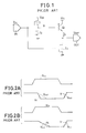
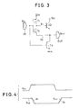
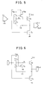
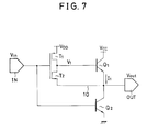
- a general object of the present invention is to provide a novel and useful Bi-CMOS inverter in which the above problems are eliminated.
Landscapes
- Engineering & Computer Science (AREA)
- Physics & Mathematics (AREA)
- Computer Hardware Design (AREA)
- Computing Systems (AREA)
- General Engineering & Computer Science (AREA)
- Mathematical Physics (AREA)
- Power Engineering (AREA)
- Logic Circuits (AREA)
- Metal-Oxide And Bipolar Metal-Oxide Semiconductor Integrated Circuits (AREA)
- Electronic Switches (AREA)
Applications Claiming Priority (2)
| Application Number | Priority Date | Filing Date | Title |
|---|---|---|---|
| JP228733/87 | 1987-09-11 | ||
| JP62228733A JPS6471325A (en) | 1987-09-11 | 1987-09-11 | Bipolar cmos inverter |
Publications (3)
| Publication Number | Publication Date |
|---|---|
| EP0307323A2 true EP0307323A2 (de) | 1989-03-15 |
| EP0307323A3 EP0307323A3 (en) | 1989-10-18 |
| EP0307323B1 EP0307323B1 (de) | 1994-07-27 |
Family
ID=16880960
Family Applications (1)
| Application Number | Title | Priority Date | Filing Date |
|---|---|---|---|
| EP88402287A Expired - Lifetime EP0307323B1 (de) | 1987-09-11 | 1988-09-09 | Inverter mit bipolarem Transistor und komplementären MOS-Transistoren |
Country Status (5)
| Country | Link |
|---|---|
| US (1) | US4882534A (de) |
| EP (1) | EP0307323B1 (de) |
| JP (1) | JPS6471325A (de) |
| KR (1) | KR910006513B1 (de) |
| DE (1) | DE3850828D1 (de) |
Cited By (5)
| Publication number | Priority date | Publication date | Assignee | Title |
|---|---|---|---|---|
| FR2686469A1 (fr) * | 1992-01-20 | 1993-07-23 | Matra Mhs | Etage de sortie ttl-cmos pour circuit integre. |
| EP0584471A3 (de) * | 1992-08-10 | 1994-03-23 | Ibm | |
| EP0678969A3 (de) * | 1994-04-18 | 1998-01-28 | Nec Corporation | BIMOS integrierte Halbleiterschaltung mit erhöherter Speisespannung |
| WO2009120200A1 (en) * | 2008-03-27 | 2009-10-01 | Agere Systems Inc. | High voltage tolerant input/output interface circuit |
| CN108370250A (zh) * | 2015-10-02 | 2018-08-03 | 索尼公司 | 半导体装置 |
Families Citing this family (10)
| Publication number | Priority date | Publication date | Assignee | Title |
|---|---|---|---|---|
| JP2783579B2 (ja) * | 1989-03-01 | 1998-08-06 | 株式会社東芝 | 半導体装置 |
| JPH02291165A (ja) * | 1989-04-29 | 1990-11-30 | Nec Corp | バイ・cmos半導体装置 |
| US4952823A (en) * | 1989-05-03 | 1990-08-28 | Advanced Micro Devices, Inc. | Bicmos decoder |
| US5155387A (en) * | 1989-12-28 | 1992-10-13 | North American Philips Corp. | Circuit suitable for differential multiplexers and logic gates utilizing bipolar and field-effect transistors |
| JP2953005B2 (ja) * | 1990-09-14 | 1999-09-27 | 日本電気株式会社 | Bi―CMOS回路 |
| US5103160A (en) * | 1991-04-25 | 1992-04-07 | Hughes Aircraft Company | Shunt regulator with tunnel oxide reference |
| JPH05167427A (ja) * | 1991-12-13 | 1993-07-02 | Toshiba Corp | レベルシフト回路 |
| DE69411312T2 (de) * | 1993-04-19 | 1999-02-11 | Philips Electronics N.V., Eindhoven | BiCMOS Ausgangstreiberschaltung |
| US5929666A (en) * | 1994-06-03 | 1999-07-27 | Lucent Technologies Inc. | Bootstrap circuit |
| JP3208296B2 (ja) * | 1995-09-12 | 2001-09-10 | シャープ株式会社 | 多値電圧出力回路および液晶駆動回路 |
Family Cites Families (6)
| Publication number | Priority date | Publication date | Assignee | Title |
|---|---|---|---|---|
| US3631528A (en) * | 1970-08-14 | 1971-12-28 | Robert S Green | Low-power consumption complementary driver and complementary bipolar buffer circuits |
| EP0058958B1 (de) * | 1981-02-25 | 1986-10-29 | Kabushiki Kaisha Toshiba | Komplementäre MOSFET-Logikschaltung |
| JPS60125015A (ja) * | 1983-12-12 | 1985-07-04 | Hitachi Ltd | インバ−タ回路 |
| JPH07107973B2 (ja) * | 1984-03-26 | 1995-11-15 | 株式会社日立製作所 | スイツチング回路 |
| EP0209805B1 (de) * | 1985-07-22 | 1993-04-07 | Hitachi, Ltd. | Halbleitereinrichtung mit bipolarem Transistor und Isolierschicht-Feldeffekttransistor |
| JPS62254460A (ja) * | 1986-04-26 | 1987-11-06 | Toshiba Corp | Bi−CMOS論理回路 |
-
1987
- 1987-09-11 JP JP62228733A patent/JPS6471325A/ja active Pending
-
1988
- 1988-08-31 US US07/238,404 patent/US4882534A/en not_active Expired - Fee Related
- 1988-09-03 KR KR1019880011394A patent/KR910006513B1/ko not_active Expired
- 1988-09-09 EP EP88402287A patent/EP0307323B1/de not_active Expired - Lifetime
- 1988-09-09 DE DE3850828T patent/DE3850828D1/de not_active Expired - Lifetime
Cited By (10)
| Publication number | Priority date | Publication date | Assignee | Title |
|---|---|---|---|---|
| FR2686469A1 (fr) * | 1992-01-20 | 1993-07-23 | Matra Mhs | Etage de sortie ttl-cmos pour circuit integre. |
| EP0553020A1 (de) * | 1992-01-20 | 1993-07-28 | Matra Mhs | TTL-CMOS-Ausgangsstufe für integrierte Schaltungen |
| US5361004A (en) * | 1992-01-20 | 1994-11-01 | Matra Mhs | TTL-CMOS output stage for an integrated circuit |
| EP0584471A3 (de) * | 1992-08-10 | 1994-03-23 | Ibm | |
| US5341042A (en) * | 1992-08-10 | 1994-08-23 | International Business Machines Corporation | Low voltage, cascoded NTL based BiCMOS circuit |
| EP0678969A3 (de) * | 1994-04-18 | 1998-01-28 | Nec Corporation | BIMOS integrierte Halbleiterschaltung mit erhöherter Speisespannung |
| WO2009120200A1 (en) * | 2008-03-27 | 2009-10-01 | Agere Systems Inc. | High voltage tolerant input/output interface circuit |
| US8310275B2 (en) | 2008-03-27 | 2012-11-13 | Agere Systems Inc. | High voltage tolerant input/output interface circuit |
| CN108370250A (zh) * | 2015-10-02 | 2018-08-03 | 索尼公司 | 半导体装置 |
| CN108370250B (zh) * | 2015-10-02 | 2022-10-11 | 索尼公司 | 半导体装置 |
Also Published As
| Publication number | Publication date |
|---|---|
| US4882534A (en) | 1989-11-21 |
| KR910006513B1 (ko) | 1991-08-27 |
| EP0307323B1 (de) | 1994-07-27 |
| DE3850828D1 (de) | 1994-09-01 |
| KR890005995A (ko) | 1989-05-18 |
| JPS6471325A (en) | 1989-03-16 |
| EP0307323A3 (en) | 1989-10-18 |
Similar Documents
| Publication | Publication Date | Title |
|---|---|---|
| US4633106A (en) | MOS bootstrap push-pull stage | |
| US4882534A (en) | Bipolar-complementary metal oxide semiconductor inverter | |
| EP0360525B1 (de) | Ausgangspufferschaltung mit einer Regelumsetzungsfunktion | |
| JPS626369B2 (de) | ||
| EP0267361A1 (de) | CMOS-Treiberschaltung mit hoher Schaltgeschwindigkeit | |
| US4740718A (en) | Bi-CMOS logic circuit | |
| JPH0436606B2 (de) | ||
| EP0361841B1 (de) | Logische Bicmos-Schaltung | |
| US4542307A (en) | Double bootstrapped clock buffer circuit | |
| EP0055073B1 (de) | Elektronische Taktsignalgeneratoren | |
| US5057713A (en) | Bipolar MOS logic circuit and semiconductor integrated circuit | |
| US4806797A (en) | bi-CMOS buffer cascaded to CMOS driver having PMOS pull-up transistor with threshold voltage greater than VBE of bi-CMOS bipolar pull-up transistor | |
| JP3151329B2 (ja) | データ出力回路 | |
| US5159214A (en) | Bicmos logic circuit | |
| EP0196616A2 (de) | Logische Schaltung | |
| JP2527050B2 (ja) | 半導体メモリ用センスアンプ回路 | |
| EP0244587B1 (de) | Komplementär-Eingangsschaltung | |
| US5751167A (en) | CMOS output buffer circuit which converts CMOS logic signals to ECL logic signals and which discharges parasitic load capacitances | |
| JP2538986B2 (ja) | 論理回路 | |
| KR940006507B1 (ko) | 출력버퍼회로 | |
| JPS61198813A (ja) | クロツクジエネレ−タ回路 | |
| JPH0681025B2 (ja) | ゲ−ト駆動回路 | |
| JP2765330B2 (ja) | 出力回路 | |
| KR940000252Y1 (ko) | 씨모스 낸드게이트 | |
| JP3171518B2 (ja) | Bimos回路 |
Legal Events
| Date | Code | Title | Description |
|---|---|---|---|
| PUAI | Public reference made under article 153(3) epc to a published international application that has entered the european phase |
Free format text: ORIGINAL CODE: 0009012 |
|
| AK | Designated contracting states |
Kind code of ref document: A2 Designated state(s): DE FR GB |
|
| PUAL | Search report despatched |
Free format text: ORIGINAL CODE: 0009013 |
|
| AK | Designated contracting states |
Kind code of ref document: A3 Designated state(s): DE FR GB |
|
| 17P | Request for examination filed |
Effective date: 19900406 |
|
| 17Q | First examination report despatched |
Effective date: 19901115 |
|
| GRAA | (expected) grant |
Free format text: ORIGINAL CODE: 0009210 |
|
| AK | Designated contracting states |
Kind code of ref document: B1 Designated state(s): DE FR GB |
|
| REF | Corresponds to: |
Ref document number: 3850828 Country of ref document: DE Date of ref document: 19940901 |
|
| PG25 | Lapsed in a contracting state [announced via postgrant information from national office to epo] |
Ref country code: GB Effective date: 19941027 |
|
| ET | Fr: translation filed | ||
| PG25 | Lapsed in a contracting state [announced via postgrant information from national office to epo] |
Ref country code: DE Effective date: 19941028 |
|
| PLBE | No opposition filed within time limit |
Free format text: ORIGINAL CODE: 0009261 |
|
| STAA | Information on the status of an ep patent application or granted ep patent |
Free format text: STATUS: NO OPPOSITION FILED WITHIN TIME LIMIT |
|
| GBPC | Gb: european patent ceased through non-payment of renewal fee |
Effective date: 19941027 |
|
| 26N | No opposition filed | ||
| PGFP | Annual fee paid to national office [announced via postgrant information from national office to epo] |
Ref country code: FR Payment date: 19950911 Year of fee payment: 8 |
|
| PG25 | Lapsed in a contracting state [announced via postgrant information from national office to epo] |
Ref country code: FR Effective date: 19960930 |
|
| REG | Reference to a national code |
Ref country code: FR Ref legal event code: ST |
|
| REG | Reference to a national code |
Ref country code: FR Ref legal event code: ST |