EP0361841B1 - Logische Bicmos-Schaltung - Google Patents
Logische Bicmos-Schaltung Download PDFInfo
- Publication number
- EP0361841B1 EP0361841B1 EP89309751A EP89309751A EP0361841B1 EP 0361841 B1 EP0361841 B1 EP 0361841B1 EP 89309751 A EP89309751 A EP 89309751A EP 89309751 A EP89309751 A EP 89309751A EP 0361841 B1 EP0361841 B1 EP 0361841B1
- Authority
- EP
- European Patent Office
- Prior art keywords
- transistor
- gate
- circuit
- input terminal
- supply line
- Prior art date
- Legal status (The legal status is an assumption and is not a legal conclusion. Google has not performed a legal analysis and makes no representation as to the accuracy of the status listed.)
- Expired - Lifetime
Links
- 238000010586 diagram Methods 0.000 description 8
- 230000000630 rising effect Effects 0.000 description 3
- 238000010276 construction Methods 0.000 description 2
- 230000003247 decreasing effect Effects 0.000 description 2
- 230000000295 complement effect Effects 0.000 description 1
- 230000007547 defect Effects 0.000 description 1
- 230000004048 modification Effects 0.000 description 1
- 238000012986 modification Methods 0.000 description 1
Images


Classifications
-
- H—ELECTRICITY
- H03—ELECTRONIC CIRCUITRY
- H03K—PULSE TECHNIQUE
- H03K19/00—Logic circuits, i.e. having at least two inputs acting on one output; Inverting circuits
- H03K19/01—Modifications for accelerating switching
- H03K19/017—Modifications for accelerating switching in field-effect transistor circuits
- H03K19/01707—Modifications for accelerating switching in field-effect transistor circuits in asynchronous circuits
- H03K19/01721—Modifications for accelerating switching in field-effect transistor circuits in asynchronous circuits by means of a pull-up or down element
-
- H—ELECTRICITY
- H03—ELECTRONIC CIRCUITRY
- H03K—PULSE TECHNIQUE
- H03K19/00—Logic circuits, i.e. having at least two inputs acting on one output; Inverting circuits
- H03K19/01—Modifications for accelerating switching
- H03K19/013—Modifications for accelerating switching in bipolar transistor circuits
- H03K19/0136—Modifications for accelerating switching in bipolar transistor circuits by means of a pull-up or down element
-
- H—ELECTRICITY
- H03—ELECTRONIC CIRCUITRY
- H03K—PULSE TECHNIQUE
- H03K19/00—Logic circuits, i.e. having at least two inputs acting on one output; Inverting circuits
- H03K19/02—Logic circuits, i.e. having at least two inputs acting on one output; Inverting circuits using specified components
- H03K19/08—Logic circuits, i.e. having at least two inputs acting on one output; Inverting circuits using specified components using semiconductor devices
- H03K19/094—Logic circuits, i.e. having at least two inputs acting on one output; Inverting circuits using specified components using semiconductor devices using field-effect transistors
- H03K19/0944—Logic circuits, i.e. having at least two inputs acting on one output; Inverting circuits using specified components using semiconductor devices using field-effect transistors using MOSFET or insulated gate field-effect transistors, i.e. IGFET
- H03K19/09448—Logic circuits, i.e. having at least two inputs acting on one output; Inverting circuits using specified components using semiconductor devices using field-effect transistors using MOSFET or insulated gate field-effect transistors, i.e. IGFET in combination with bipolar transistors [BIMOS]
Definitions
- the present invention relates to a BiCMOS logic circuit, and more specifically to a BiCMOS logic circuit having a high operation speed.
- BiCMOS logic circuits have been composed of an input MOS logic circuit and an output bipolar circuit.
- a base current for a bipolar transistor for extracting the electric charge on the output of the bipolar circuit is supplied by only a MOS transistor whose gate is connected to a logic input of the input MOS logic circuit and whose drain-source path is connected between a collector and the base of the charge extracting bipolar transistor.
- the BiCMOS logic circuit has a large delay time, and a long signal propagation time.
- EP-A-0.261.528 discloses a logic circuit in which a base current supply for a bipolar output transistor is derived in part from a control MOS transistor coupled between a power source terminal and the base of the bipolar transistor.
- Another object of the present invention is to provide a BiCMOS logic circuit having a shortened signal propagation time when an output voltage decays.
- a BiCMOS logic circuit which includes an input terminal, an output terminal, a MOS logic circuit connected between a first voltage supply line and a second voltage supply line and having an input connected to the input terminal, and an output circuit composed of first and second bipolar transistors connected in series between the first voltage supply line and the second voltage supply line, the first bipolar transistor having a base connected to an output of the MOS logic circuit, a connection node of the first and second bipolar transistors being connected to the output terminal, and a base current supplying circuit having first and second MOS transistors connected in series between the first voltage supply line and a base of the second bipolar transistor, the first MOS transistor having a gate connected to the output of the MOS logic circuit, the second MOS transistor having a gate connected to the input terminal, said base current supplying circuit further including a third MOS transistor connected between said base of said second bipolar transistor and said connection node of said first and second bipolar transistors and having a gate connected to said input terminal
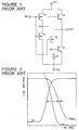
- the shown conventional BiCMOS logic circuit comprises a complementary MOS (CMOS) inverter composed of a PMOS transistor 10 and a NMOS transistor 12 connected in series between a high voltage supply line V CC and a low voltage supply line V EE .
- CMOS complementary MOS
- a source of the PMOS transistor 10 is connected to the high voltage supply line V CC
- a source of the NMOS transistor 12 is connected to the low voltage supply line V EE .
- Gates of these MOS transistors are connected to an input terminal IN. Drains of the PMOS transistor 10 and the NMOS transistor 12 are connected to each other and forms an output node N1 of the CMOS inverter.
- the BiCMOS logic circuit also includes a bipolar output circuit composed of two NPN bipolar transistors 14 and 16 connected in series between the high voltage supply line V CC and the low voltage supply line V EE .
- the bipolar transistor 14 has a collector connected to the high voltage supply line V CC , and an emitter connected to a collector of the bipolar transistor 16, whose emitter is connected to the low voltage supply line V EE .
- a base of the bipolar transistor 14 connected to the output node N1 of the CMOS inverter.
- a NMOS transistor 18 is connected between the collector and a base of the bipolar transistor 16 connected to the low voltage supply line V EE in such a manner that a drain of the NMOS transistor 18 is connected to the collector of the bipolar transistor 16 and a source of the NMOS transistor 18 is connected to the base of the bipolar transistor 16.
- a gate of the NMOS transistor 18 is connected to the input terminal IN.
- the base of the bipolar transistor 16 is connected to the low voltage supply line V EE through a resistor 20.
- the connection node between the two NPN bipolar transistors 14 and 16 is connected to an output terminal OUT of the BiCMOS logic circuit.
- the base of the bipolar transistor 16 is called a node N2 hereinafter.
- BiCMOS logic circuit when a potential on the output terminal OUT is fallen down, an electric charge on the output terminal OUT is extracted through the bipolar transistor 16 connected to the low voltage supply line V EE .
- a base current for bringing the transistor 16 conductive is supplied by the NMOS transistor 18 which is connected between the collector and the base of the bipolar transistor 16 and which receives at the base thereof an input signal on the input terminal IN.
- the collector-base voltage of the transistor 16 is rendered small as a result of the drop of the voltage on the output terminal OUT
- the source-drain voltage of the NMOS transistor 18 is correspondingly rendered small.
- the NMOS transistor 18 will operate in a linear operation region, so that the NMOS transistor 18 can no longer supply a sufficient base current to the bipolar transistor 16. Accordingly, the falling speed of the potential of the ouput terminal OUT becomes low, with the result that the BiCMOS logic circuit has a substantial delay time.
- FIG. 2 shows variations of a voltage V IN on the input terminal IN, a voltage V OUT on the output terminal OUT, and a voltage V N1 on the output node N1 of the CMOS inverter.
- the voltage V N1 quickly falls down in response to a rising of the voltage V IN , the voltage V OUT drops with a delay. Namely, a propagation delay time tpd is large. The reason for this is that a sufficient base current is not supplied to the bipolar transistor 16, and therefore, a collector current of the bipolar transistor 16 is restricted to a low value.
- a gate width and a gate length of the PMOS transistor 10 and the NMOS transistors 12 and 18 are 20 ⁇ m and 1.5 ⁇ m, 5 ⁇ m and 1.3 ⁇ m, and 10 ⁇ m and 1.3 ⁇ m, respectively, and an emitter area of each of the bipolar transistors 14 and 16 are 7.2 ⁇ m.
- the resister 20 has 20K ⁇ and a supply voltage (between V CC and V EE ) is 4.5V. In this case, the delay time tpd becomes 0.63ns.
- FIG 3 there is shown a circuit diagram of a first embodiment of the BiCMOS logic circuit in accordance with the present invention.
- elements similar to those shown in Figure 1 are given the same Reference Numerals, and explanation thereof will be omitted for simplification.
- the circuit shown in Figure 3 includes a series circuit composed of NMOS transistors 22 and 24 in addition to the circuit shown in Figure 1.
- the NMOS transistor 22 has a drain connected to the high voltage supply line V CC , and a gate connected to the output node N1 of the CMOS inverter.
- a source of the NMOS transistor 22 is connected to a drain of the NMOS transistor 24, which is connected at a source thereof to the node N2, namely the base of the bipolar transistor 16.
- a gate of the NMOS transistor 24 is connected to the input terminal 10.
- Figure 4 illustrates variations of a voltage V IN on the input terminal IN, a voltage V OUT on the output terminal OUT, and a voltage V N1 on the output node N1 of the CMOS inverter in the circuit shown in Figure 3.
- the voltage V N1 on the output node N1 of the CMOS inverter starts to fall down with a short and determined time delay after the moment the input signal V1 starts to rise up.
- the NMOS transistor 24 is turned on at a moment t1, and thereafter, as a result of the falling of the node voltage V N1 , the NMOS transistor 22 is turned off at a moment t2. Therefore, for a period of time to from the moment t1 to the moment t2, a current is supplied directly to the base of the bipolar transistor 16 through the two series-connected NMOS transistors 22 and 24 from the high voltage supply line V CC , in addition to a conventional base current supply path formed of the transistor 18. Accordingly, the base current of the bipolar transistor 16 is increased, and therefore, the collector current of the bipolar transistor 16 is correspondingly increased. As a result, the speed of extracting the electric charge from the output terminal OUT is increased, and accordingly, the propagation delay time tpd is decreased.
- a gate width and a gate length of the PMOS transistor 10 and the NMOS transistors 12, 18, 22 and 24 are 20 ⁇ m and 1.5 ⁇ m, 5 ⁇ m and 1.3 ⁇ m, 10 ⁇ m and 1.3 ⁇ m, 20 ⁇ m and 1.3 ⁇ m, and 20 ⁇ m and 1.3 ⁇ m, respectively, and an emitter area of each of the bipolar transistors 14 and 16 are 7.2 ⁇ m.
- the resister 20 has 20K ⁇ and a supply voltage is 4.5V. In this case, the delay time tpd becomes 0.48ns, which has been reduced from that of the circuit shown in Figure 1 by 24%.
- FIG. 5 there is shown a circuit diagram of a second embodiment of the BiCMOS logic circuit in accordance with the present invention.
- This BiCMOS logic circuit forms a two-input NOR circuit.
- the shown BiCMOS circuit comprises a two-input CMOS NOR circuit, which includes a first PMOS transistor 30 having a gate 54 connected to a first input terminal IN1 and a source connected to a high voltage supply line V CC , and a second PMOS transistor 32 having a gate 56 connected to a second input terminal IN2 and a source connected to a drain of the first PMOS transistor 30.
- the two-input CMOS NOR circuit also includes a first NMOS transistor 34 having a gate 58 connected to the first input terminal IN1, a drain connected to a drain of the second PMOS transistor 32, and a source connected to a low voltage supply line V EE , and a second NMOS transistor 36 having a gate 60 connected to the second input terminal IN2, a drain connected to the drain of the second PMOS transistor 32, and a source connected to the low voltage supply line V EE .
- a connection node N1 between the PMOS transistor 32 and the two NMOS transistors 34 and 36 forms an output node of the CMOS NOR circuit.
- the shown BiCMOS circuit further comprises a bipolar output circuit composed of a first NPN bipolar transistor 38 having a collector connected to the high voltage supply line V CC and a base connected to output node N1 of the CMOS NOR circuit, and a second NPN bipolar transistor 40 having a collector connected to an emitter of the NPN bipolar transistor 38 and an emitter connected to the low voltage supply line V EE .
- a base of the second NPN bipolar transistor 40 is connected through a resister 42 to the low voltage supply line V EE .
- two NMOS transistors 44 and 46 are connected between the collector and the base of the second NPN bipolar transistor 40.
- a gate of the NMOS transistors 44 is connected to the first input terminal IN1, and a gate of the NMOS transistors 46 is connected to the second input terminal IN2.
- the connection node between the bipolar transistors 38 and 40 is connected to an output terminal OUT.
- the shown BiCMOS circuit includes a series circuit composed of a NMOS transistor 52 and a parallel circuit of two NMOS transistors 48 and 50, as shown in Figure 5.
- the series circuit is connected between the high voltage supply line V CC and the base N2 of the bipolar transistor 40.
- a drain of the NMOS transistor 52 is connected to the high voltage supply line V CC and a gate of the NMOS transistor 52 is connected to the node N1 of the CMOS NOR circuit.
- a source of the NMOS transistor 52 is connected commonly to drains of the NMOS transistors 48 and 50, whose sources are commonly connected to the base N2 of the bipolar transistor 40.
- a gate of the NMOS transistor 48 is connected to the first input terminal IN1 and a gate of the NMOS transistor 50 is connected to the second input terminal IN2.
- the NMOS transistor 48 (or 50) is turned on in the course of the rising of the first input signal voltage V IN1 (or the second input signal voltage V IN2 ).
- a current path passing through the NMOS transistor 52 and the NMOS transistor 48 (or 50) is formed to supply an additional base current from the high voltage supply line to the base of the bipolar transistor 40. Namely, the base current of the bipolar transistor 40 is increased. This condition is maintained for a constant period of time until the NMOS transistor 52 is turned off as a result of the voltage falling of the output node N1 of the CMOS NOR circuit. Therefore, a collector current of the bipolar transistor 40 is correspondingly increased, and accordingly, the propagation time tpd is rendered small.
- the BiCMOS logic circuit in accordance with the present invention is characterized by provision of an additional base current supplying circuit connected between a high voltage supply line and a base of a bipolar transistor for extracting electric charges on the output terminal.
- the additional base current supplying circuit has first and second control inputs connected to an input and an output of a MOS logic circuit, respectively, so that the additional base current supplying circuit operates to supply an additional base current to the base of the electric charge extracting bipolar transistor from the high voltage supply line for a constant time after a logical level on said input terminal starts to change, utilizing the fact that the potential of the output of the MOS logic circuit will change with a little but constant delay from a voltage change of the input of the MOS logic circuit.
- a a result the signal propagation time of the BiCMOS logic circuit when the output terminal potential is fallen down can be made small.
Landscapes
- Engineering & Computer Science (AREA)
- Physics & Mathematics (AREA)
- Computer Hardware Design (AREA)
- Computing Systems (AREA)
- General Engineering & Computer Science (AREA)
- Mathematical Physics (AREA)
- Power Engineering (AREA)
- Logic Circuits (AREA)
- Electronic Switches (AREA)
Claims (6)
- Logische BiCMOS(bipolare CMOS)-Schaltung, die einschließt:einen Eingangsanschluß (IN; IN1+IN2);einen Ausgangsanschluß (OUT);eine logische MOS-Schaltung, die zwischen einer ersten Spannungsversorgungsleitung (VCC) und einer zweiten Spannungsversorgungsleitung (VEE) verbunden ist und die mit einem Eingang (6 und 8; 54+56 und 58+60) mit dem Eingangsanschluß (IN; IN1+IN2) verbunden ist; undeine Ausgangsschaltung, die aus ersten und zweiten bipolaren Transistoren (14 und 16; 38 und 40) aufgebaut ist, die in Reihe zwischen der ersten Spannungsversorgungsleitung (VCC) und der zweiten Spannungsversorgungsleitung (VEE) verbunden sind, wobei der erste bipolare Transistor (14; 38) mit seiner Basis mit einem Ausgang (N1) der logischen MOS-Schaltung verbunden ist, wobei ein Verbindungspunkt der ersten und zweiten bipolaren Transistoren mit dem Ausgangsanschluß verbunden ist;
dadurch gekennzeichnet, daß sie eine Basisstromversorgungsschaltung mit ersten und zweiten MOS-Transistoren (22 und 24; 52 und 48+50) aufweist, die in Reihe zwischen der ersten Spannungsversorgungsleitung und der Basis des zweiten bipolaren Transistors (16; 40) verbunden sind, wobei der erste MOS-Transistor (22; 52) mit dem Gatter mit dem Ausgang (N1) der logischen MOS-Schaltung verbunden ist, wobei der zweite MOS-Transistor (24; 48+50) mit dem Gatter mit dem Eingangsanschluß verbunden ist, wobei die Basisstromversorgungsschaltung weiter einen dritten MOS-Transistor (18; 44+46) einschließt, der zwischen der Basis des zweiten bipolaren Transistors (16; 40) und dem Verbindungspunkt der ersten und zweiten bipolaren Transistoren verbunden ist und mit dem Gatter mit dem Eingangsanschluß (IN; IN1+IN2) verbunden ist, wobei die Basis des zweiten bipolaren Transistors durch einen Widerstand (20; 42) mit der zweiten Spannungsversorgungsleitung verbunden ist. - Logische BiCMOS-Schaltung nach Anspruch 1, bei der die logische MOS-Schaltung ein CMOS-Inverter (10,12) ist.
- Logische BiCMOS-Schaltung nach Anspruch 2, bei der der CMOS-Inverter einen PMOS-Transistor (10), der mit der Quelle mit der ersten Spannungsversorgungsleitung (VCC) und mit dem Gatter (6) mit dem Eingangsanschluß (IN; IN1, IN2) verbunden ist, und einen NMOS-Transistor (12) einschließt, der mit der Quelle mit der zweiten Spannungsversorgungsleitung (VEE) und mit dem Gatter (8) mit dem Eingangsanschluß verbunden ist, wobei die Senken des PMOS-Transistors und des NMOS-Transistors miteinander verbunden sind, um einen Ausgang (N1) des CMOS-Inverters zu bilden.
- Logische BiCMOS-Schaltung nach Anspruch 1, bei der die logische MOS-Schaltung eine NOR-Schaltung (30,32) mit zwei Eingängen ist.
- Logische BiCMOS-Schaltung nach Anspruch 4, bei der die beiden Eingangs-NOR-Schaltungen erste und zweite Eingangsanschlüsse (IN1,IN2), einen ersten PMOS-Transistor (30), der mit der Quelle mit der ersten Spannungsversorgungsleitung (VCC) und mit dem Gatter (54) mit dem ersten Eingangsanschluß verbunden ist, einen zweiten PMOS-Transistor (32), der mit der Quelle mit der Senke des ersten PMOS-Transistors (30) und mit dem Gatter (56) mit dem zweiten Eingangsanschluß verbunden ist, und erste und zweite NMOS-Transistoren einschließt, die jeweils mit der Quelle mit der zweiten Spannungsversorgungsleitung (VEE) und der Senke gemeinsam mit der Senke des zweiten PMOS-Transistors verbunden sind, wobei das Gatter (58) des erten NMOS-Transistors mit dem ersten Eingangsanschluß verbunden ist, wobei das Gatter (60) des zweiten NMOS-Transistors mit dem zweiten Eingangsanschluß verbunden ist, wobei ein Verbindungspunkt zwischen der Senke des zweiten PMOS-Transistors und der gemeinsam verbundenen Senken der ersten und zweiten NMOS-Transistoren einen Ausgang (N1) der NOR-Schaltung mit zwei Eingängen bildet, und wobei der dritte MOS-Transistor (44,46) parallel zu dem zweiten Transistor (32) verbunden ist, wobei das Gatter des ersten MOS-Transistors (52) mit dem Ausgang der NOR-Schaltung mit zwei Eingängen verbunden ist, wobei das Gatter des zweiten MOS-Transistors (48,50) mit dem ersten Eingangsanschluß und das Gatter des dritten MOS-Transistors mit dem zweiten Eingangsanschluß verbunden ist.
- Logische BiCMOS-Schaltung nach Anspruch 5, die weiter vierte und fünfte MOS-Transistoren einschließt, die parallel zwischen der Basis des zweiten bipolaren Transistors und dem Verbindungspunkt der ersten und zweiten bipolaren Transistoren verbunden sind, wobei das Gatter des vierten MOS-Transistors mit dem ersten Eingangsanschluß und das Gatter des fünften MOS-Transistors mit dem zweiten Eingangsanschluß verbunden ist und die Basis des zweiten bipolaren Transistors durch einen Widerstand mit der zweiten Spannungsversorgungsleitung verbunden ist.
Applications Claiming Priority (2)
| Application Number | Priority Date | Filing Date | Title |
|---|---|---|---|
| JP240176/88 | 1988-09-26 | ||
| JP63240176A JP2696991B2 (ja) | 1988-09-26 | 1988-09-26 | BiCMOS論理回路 |
Publications (3)
| Publication Number | Publication Date |
|---|---|
| EP0361841A2 EP0361841A2 (de) | 1990-04-04 |
| EP0361841A3 EP0361841A3 (en) | 1990-10-31 |
| EP0361841B1 true EP0361841B1 (de) | 1996-03-06 |
Family
ID=17055604
Family Applications (1)
| Application Number | Title | Priority Date | Filing Date |
|---|---|---|---|
| EP89309751A Expired - Lifetime EP0361841B1 (de) | 1988-09-26 | 1989-09-26 | Logische Bicmos-Schaltung |
Country Status (4)
| Country | Link |
|---|---|
| US (1) | US4985645A (de) |
| EP (1) | EP0361841B1 (de) |
| JP (1) | JP2696991B2 (de) |
| DE (1) | DE68925856T2 (de) |
Cited By (1)
| Publication number | Priority date | Publication date | Assignee | Title |
|---|---|---|---|---|
| CN105915211A (zh) * | 2016-05-17 | 2016-08-31 | 深圳芯能半导体技术有限公司 | 非重叠电路和高压驱动电路 |
Families Citing this family (13)
| Publication number | Priority date | Publication date | Assignee | Title |
|---|---|---|---|---|
| JPH043619A (ja) * | 1990-04-20 | 1992-01-08 | Toshiba Corp | 半導体集積回路 |
| KR930004353B1 (ko) * | 1990-04-26 | 1993-05-26 | 한국전기통신공사 | BiCMOS의 제삼상태 출력회로 |
| JPH0420121A (ja) * | 1990-05-15 | 1992-01-23 | Fujitsu Ltd | Bi―CMOS回路 |
| US5153464A (en) * | 1990-12-14 | 1992-10-06 | Hewlett-Packard Company | Bicmos tri-state output buffer |
| US5077490A (en) * | 1991-01-30 | 1991-12-31 | Northern Telecom Limited | Schottky-diode emulator for BiCMOS logic circuit |
| US5132567A (en) * | 1991-04-18 | 1992-07-21 | International Business Machines Corporation | Low threshold BiCMOS circuit |
| US5191239A (en) * | 1991-12-19 | 1993-03-02 | Sun Microsystems, Inc. | Reset gate for a phase detector in a phase-locked loop |
| KR940007954B1 (ko) * | 1992-03-06 | 1994-08-29 | 삼성전자 주식회사 | BiCMOS 구동회로 |
| US5287021A (en) * | 1992-05-06 | 1994-02-15 | Motorola, Inc. | Low noise BICMOS circuit |
| US5355030A (en) * | 1992-12-04 | 1994-10-11 | International Business Machines Corporation | Low voltage BICMOS logic switching circuit |
| US5332933A (en) * | 1993-01-21 | 1994-07-26 | Hewlett-Packard Company | Bipolar-MOS circuits with dimensions scaled to enhance performance |
| US5438270A (en) * | 1994-06-24 | 1995-08-01 | National Semiconductor Corporation | Low battery tester comparing load and no-load battery voltage |
| EP1776970A1 (de) * | 2005-10-12 | 2007-04-25 | Albert Schömig | Implantat mit Mehrfachbeschichtung |
Family Cites Families (10)
| Publication number | Priority date | Publication date | Assignee | Title |
|---|---|---|---|---|
| JPS60125015A (ja) * | 1983-12-12 | 1985-07-04 | Hitachi Ltd | インバ−タ回路 |
| JPH0616585B2 (ja) * | 1983-12-16 | 1994-03-02 | 株式会社日立製作所 | バツフア回路 |
| JPH07107973B2 (ja) * | 1984-03-26 | 1995-11-15 | 株式会社日立製作所 | スイツチング回路 |
| US4616146A (en) * | 1984-09-04 | 1986-10-07 | Motorola, Inc. | BI-CMOS driver circuit |
| US4638186A (en) * | 1985-12-02 | 1987-01-20 | Motorola, Inc. | BIMOS logic gate |
| US4649294A (en) * | 1986-01-13 | 1987-03-10 | Motorola, Inc. | BIMOS logic gate |
| JPS6362411A (ja) * | 1986-09-02 | 1988-03-18 | Nec Corp | 半導体回路 |
| JPS6382122A (ja) * | 1986-09-26 | 1988-04-12 | Toshiba Corp | 論理回路 |
| US4839537A (en) * | 1986-11-29 | 1989-06-13 | Kabushiki Kaisha Toshiba | BicMO logic circuit |
| JPS63202126A (ja) * | 1987-02-17 | 1988-08-22 | Toshiba Corp | 論理回路 |
-
1988
- 1988-09-26 JP JP63240176A patent/JP2696991B2/ja not_active Expired - Lifetime
-
1989
- 1989-09-26 EP EP89309751A patent/EP0361841B1/de not_active Expired - Lifetime
- 1989-09-26 US US07/412,814 patent/US4985645A/en not_active Expired - Fee Related
- 1989-09-26 DE DE68925856T patent/DE68925856T2/de not_active Expired - Fee Related
Cited By (1)
| Publication number | Priority date | Publication date | Assignee | Title |
|---|---|---|---|---|
| CN105915211A (zh) * | 2016-05-17 | 2016-08-31 | 深圳芯能半导体技术有限公司 | 非重叠电路和高压驱动电路 |
Also Published As
| Publication number | Publication date |
|---|---|
| EP0361841A2 (de) | 1990-04-04 |
| JPH0287819A (ja) | 1990-03-28 |
| US4985645A (en) | 1991-01-15 |
| JP2696991B2 (ja) | 1998-01-14 |
| DE68925856D1 (de) | 1996-04-11 |
| DE68925856T2 (de) | 1996-08-01 |
| EP0361841A3 (en) | 1990-10-31 |
Similar Documents
| Publication | Publication Date | Title |
|---|---|---|
| US5208489A (en) | Multiple compound domino logic circuit | |
| US4845386A (en) | Bi-MOS logic circuit having a totem pole type output buffer section | |
| US5047669A (en) | Tristate circuit using bipolar transistor and CMOS transistor | |
| EP0361841A2 (de) | Logische Bicmos-Schaltung | |
| US5559451A (en) | Bicmos push-pull type logic apparatus with voltage clamp circuit and clamp releasing circuit | |
| US5663659A (en) | Semiconductor integrated circuit device comprising CMOS transistors and differentiator | |
| US4740718A (en) | Bi-CMOS logic circuit | |
| EP0307323B1 (de) | Inverter mit bipolarem Transistor und komplementären MOS-Transistoren | |
| KR900000487B1 (ko) | 논리 게이트 회로 | |
| US4289978A (en) | Complementary transistor inverting emitter follower circuit | |
| EP0768762B1 (de) | Ausgangsschaltung | |
| US4880998A (en) | Bipolar transistor and CMOS transistor logic circuit having improved discharge capabilities | |
| US5254885A (en) | Bi-CMOS logic circuit with feedback | |
| US5057713A (en) | Bipolar MOS logic circuit and semiconductor integrated circuit | |
| US5159214A (en) | Bicmos logic circuit | |
| EP0426547A2 (de) | Bi-CMOS-Schaltung | |
| EP0432472A2 (de) | Integrierte CMOS-Ausgangsschaltung mit bipolaren Transistoren in der Ausgangsstufe | |
| EP0303257A1 (de) | Schaltung zur Erzeugung eines Rücksetzsignals | |
| EP0054408B1 (de) | Logikschaltung | |
| JP2538986B2 (ja) | 論理回路 | |
| US5247214A (en) | Bi-cmos out buffer circuit for cmos logic | |
| JP3008426B2 (ja) | BiCMOSゲート回路 | |
| JP3099351B2 (ja) | BiCMOS論理回路 | |
| JP2641261B2 (ja) | バッファ回路 | |
| EP0250007A2 (de) | TTL-Pufferschaltung |
Legal Events
| Date | Code | Title | Description |
|---|---|---|---|
| PUAI | Public reference made under article 153(3) epc to a published international application that has entered the european phase |
Free format text: ORIGINAL CODE: 0009012 |
|
| 17P | Request for examination filed |
Effective date: 19891010 |
|
| AK | Designated contracting states |
Kind code of ref document: A2 Designated state(s): DE FR GB |
|
| PUAL | Search report despatched |
Free format text: ORIGINAL CODE: 0009013 |
|
| AK | Designated contracting states |
Kind code of ref document: A3 Designated state(s): DE FR GB |
|
| 17Q | First examination report despatched |
Effective date: 19930709 |
|
| GRAA | (expected) grant |
Free format text: ORIGINAL CODE: 0009210 |
|
| AK | Designated contracting states |
Kind code of ref document: B1 Designated state(s): DE FR GB |
|
| REF | Corresponds to: |
Ref document number: 68925856 Country of ref document: DE Date of ref document: 19960411 |
|
| ET | Fr: translation filed | ||
| PLBE | No opposition filed within time limit |
Free format text: ORIGINAL CODE: 0009261 |
|
| STAA | Information on the status of an ep patent application or granted ep patent |
Free format text: STATUS: NO OPPOSITION FILED WITHIN TIME LIMIT |
|
| 26N | No opposition filed | ||
| PGFP | Annual fee paid to national office [announced via postgrant information from national office to epo] |
Ref country code: FR Payment date: 20000912 Year of fee payment: 12 |
|
| PGFP | Annual fee paid to national office [announced via postgrant information from national office to epo] |
Ref country code: DE Payment date: 20000918 Year of fee payment: 12 |
|
| PGFP | Annual fee paid to national office [announced via postgrant information from national office to epo] |
Ref country code: GB Payment date: 20000920 Year of fee payment: 12 |
|
| PG25 | Lapsed in a contracting state [announced via postgrant information from national office to epo] |
Ref country code: GB Free format text: LAPSE BECAUSE OF NON-PAYMENT OF DUE FEES Effective date: 20010926 |
|
| REG | Reference to a national code |
Ref country code: GB Ref legal event code: IF02 |
|
| PG25 | Lapsed in a contracting state [announced via postgrant information from national office to epo] |
Ref country code: DE Free format text: LAPSE BECAUSE OF NON-PAYMENT OF DUE FEES Effective date: 20020501 |
|
| GBPC | Gb: european patent ceased through non-payment of renewal fee |
Effective date: 20010926 |
|
| PG25 | Lapsed in a contracting state [announced via postgrant information from national office to epo] |
Ref country code: FR Free format text: LAPSE BECAUSE OF NON-PAYMENT OF DUE FEES Effective date: 20020531 |
|
| REG | Reference to a national code |
Ref country code: FR Ref legal event code: ST |