EP0308128A1 - Verfahren zur Herstellung von Dünnschicht Transistoren - Google Patents
Verfahren zur Herstellung von Dünnschicht Transistoren Download PDFInfo
- Publication number
- EP0308128A1 EP0308128A1 EP88308261A EP88308261A EP0308128A1 EP 0308128 A1 EP0308128 A1 EP 0308128A1 EP 88308261 A EP88308261 A EP 88308261A EP 88308261 A EP88308261 A EP 88308261A EP 0308128 A1 EP0308128 A1 EP 0308128A1
- Authority
- EP
- European Patent Office
- Prior art keywords
- layer
- gate electrodes
- transparent
- depositing
- conductive
- Prior art date
- Legal status (The legal status is an assumption and is not a legal conclusion. Google has not performed a legal analysis and makes no representation as to the accuracy of the status listed.)
- Withdrawn
Links
Images


Classifications
-
- H—ELECTRICITY
- H10—SEMICONDUCTOR DEVICES; ELECTRIC SOLID-STATE DEVICES NOT OTHERWISE PROVIDED FOR
- H10D—INORGANIC ELECTRIC SEMICONDUCTOR DEVICES
- H10D99/00—Subject matter not provided for in other groups of this subclass
-
- H—ELECTRICITY
- H10—SEMICONDUCTOR DEVICES; ELECTRIC SOLID-STATE DEVICES NOT OTHERWISE PROVIDED FOR
- H10D—INORGANIC ELECTRIC SEMICONDUCTOR DEVICES
- H10D30/00—Field-effect transistors [FET]
- H10D30/60—Insulated-gate field-effect transistors [IGFET]
- H10D30/67—Thin-film transistors [TFT]
- H10D30/6729—Thin-film transistors [TFT] characterised by the electrodes
- H10D30/673—Thin-film transistors [TFT] characterised by the electrodes characterised by the shapes, relative sizes or dispositions of the gate electrodes
- H10D30/6733—Multi-gate TFTs
- H10D30/6734—Multi-gate TFTs having gate electrodes arranged on both top and bottom sides of the channel, e.g. dual-gate TFTs
-
- H—ELECTRICITY
- H10—SEMICONDUCTOR DEVICES; ELECTRIC SOLID-STATE DEVICES NOT OTHERWISE PROVIDED FOR
- H10D—INORGANIC ELECTRIC SEMICONDUCTOR DEVICES
- H10D30/00—Field-effect transistors [FET]
- H10D30/60—Insulated-gate field-effect transistors [IGFET]
- H10D30/67—Thin-film transistors [TFT]
- H10D30/674—Thin-film transistors [TFT] characterised by the active materials
- H10D30/675—Group III-V materials, Group II-VI materials, Group IV-VI materials, selenium or tellurium
-
- Y—GENERAL TAGGING OF NEW TECHNOLOGICAL DEVELOPMENTS; GENERAL TAGGING OF CROSS-SECTIONAL TECHNOLOGIES SPANNING OVER SEVERAL SECTIONS OF THE IPC; TECHNICAL SUBJECTS COVERED BY FORMER USPC CROSS-REFERENCE ART COLLECTIONS [XRACs] AND DIGESTS
- Y10—TECHNICAL SUBJECTS COVERED BY FORMER USPC
- Y10S—TECHNICAL SUBJECTS COVERED BY FORMER USPC CROSS-REFERENCE ART COLLECTIONS [XRACs] AND DIGESTS
- Y10S148/00—Metal treatment
- Y10S148/106—Masks, special
Definitions
- This invention relates to semiconductor devices and methods of manufacture thereof. In particular, it is concerned with the fabrication of thin film transistors having a pair of gate electrodes disposed about a channel region.
- a substrate which may be composed of the semiconductor itself or may be an insulating support for active materials which are deposited as thin films on the surface of the substrate.
- Active devices comprise a plurality of regions having different conducting properties to which conductive electrodes are applied.
- a method of manufacture of semiconductor devices comprising the steps of depositing on the surface of a transparent insulating substrate a first layer of conductive material adapted to form a first plurality of gate electrodes, depositing over said first layer of conductive material, a first layer of transparent insulating material, forming on the exposed surface of said first layer of insulating material a plurality of pairs of conductive contacts having gaps therebetween defined by photolithography involving exposure to radiation through said transparent insulation substrate using said first plurality of gate electrodes as a mask, depositing a layer of semiconductive material to form a semiconductive path between said pairs of conductive contacts.
- a method of manufacture of semiconductor devices comprising the steps of depositing on the surface of a transparent insulating substrate a first layer of conductive material adapted to form a first plurality of gate electrodes, depositing over said first layer of conductive material, a first layer of transparent insulating material, forming on the exposed surface of said first layer of insulating material a plurality of pairs of conductive contacts having gaps therebetween defined by photolithography involving exposure to radiation through said transparent insulation substrate using said first plurality of gate electrodes as a mask, depositing a layer of semiconductive material to form a semiconductive path between said pairs of conductive contacts, further depositing over said layer of semiconductive material and said conductive contacts a second layer of transparent insulating material, and depositing on said second layer of transparent insulating material a second plurality of gate electrodes having an area defined by photolithography involving exposure to radiation through said transparent insulation substrate using said first plurality of gate electrodes as a mask.
- the layer of semiconductive material may be deposited either before or after the conductive contacts.
- a field-effect device comprising a channel region of semiconductor material having a pair of transparent conductive contacts thereto and a pair of gate electrodes positioned on opposite sides of said channel region each of said gate electrodes being insulated therefrom by a layer of insulating material wherein the edge adjoining said channel region of each of said electrodes is substantially coplanar with the corresponding edges of said gate electrodes.
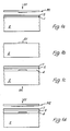
- a layer of chromium 1 is deposited in vacuo on to a transparent glass substrate 2.
- a layer of photoresist 3 is spun on to the chromium and exposed to ultra-violet radiation UV through a mask M1.
- the resist is developed and the chromium selectively etched leaving an array of gate electrodes G1.
- Figure 1b An insulating layer of silicon dioxide 4 followed by a layer of a transparent, conductive material such as indium/tin oxide 5 is then deposited on to the substrate.
- This is then covered with a further layer of photoresist 7 which is exposed to ultra-violet radiation through the substrate such that on development the photoresist is removed over the area of the opaque gate electrodes.
- the exposed conductive area is etched.
- the substrate is then heat-treated in a hydrogen-nitrogen ambient to render the indium/tin oxide layer highly conductive.
- a layer of cadmium selenide 9 and a further layer of photoresist 10 is deposited on to the insulator 4 and the defined contacts 5 on the substrate 2. This photoresist is exposed to ultra-violet radiation UV through another non-critical mask M3.
- the cadmium selenide layer is etched to form channel regions C.
- a second insulating layer of silicon dioxide 12 and yet another layer of photoresist 13 are deposited and exposed to ultra-violet radiation UV through the substrate.
- Both the cadmium selenide and the indium/tin oxide layers are transparent to ultra-violet radiation, but the first gate array acts as mask, so that when the resist is developed, windows corresponding exactly to the pattern of the first gate array are formed.
- a layer 14 of nickel is then deposited and the remaining photoresist removed leaving a second gate array G2 of exactly the same dimensions as those of the first gate array G1.
- the method of exposure of photoresist through the transparent substrate using the opaque patterns deposited thereon as a mask to achieve precise alignment and minimum parasitic capacitance may be used to produce devices with only one gate electrode.
- the second gate electrode need not have any electrical effect and may serve simply for optical screening of the photosensitive channel region.
- the semiconductor material used for the device is preferably a II-VI compound, but other materials suitable for thin film transistor fabrication may be used. Other materials may be used for the electrodes.
Landscapes
- Thin Film Transistor (AREA)
Applications Claiming Priority (2)
| Application Number | Priority Date | Filing Date | Title |
|---|---|---|---|
| GB8721193 | 1987-09-09 | ||
| GB878721193A GB8721193D0 (en) | 1987-09-09 | 1987-09-09 | Semiconductor devices |
Publications (1)
| Publication Number | Publication Date |
|---|---|
| EP0308128A1 true EP0308128A1 (de) | 1989-03-22 |
Family
ID=10623506
Family Applications (1)
| Application Number | Title | Priority Date | Filing Date |
|---|---|---|---|
| EP88308261A Withdrawn EP0308128A1 (de) | 1987-09-09 | 1988-09-07 | Verfahren zur Herstellung von Dünnschicht Transistoren |
Country Status (5)
| Country | Link |
|---|---|
| US (1) | US4968638A (de) |
| EP (1) | EP0308128A1 (de) |
| JP (1) | JPH01152763A (de) |
| CA (1) | CA1308495C (de) |
| GB (2) | GB8721193D0 (de) |
Cited By (2)
| Publication number | Priority date | Publication date | Assignee | Title |
|---|---|---|---|---|
| WO1993021659A1 (en) * | 1992-04-15 | 1993-10-28 | British Technology Group Ltd. | Semiconductor devices with a double gate |
| WO1997005648A1 (en) * | 1995-07-31 | 1997-02-13 | Litton Systems Canada Limited | Method of forming self-aligned thin film transistor |
Families Citing this family (13)
| Publication number | Priority date | Publication date | Assignee | Title |
|---|---|---|---|---|
| JPH0242761A (ja) * | 1988-04-20 | 1990-02-13 | Matsushita Electric Ind Co Ltd | アクティブマトリクス基板の製造方法 |
| US5079606A (en) * | 1989-01-26 | 1992-01-07 | Casio Computer Co., Ltd. | Thin-film memory element |
| DE69125886T2 (de) * | 1990-05-29 | 1997-11-20 | Semiconductor Energy Lab | Dünnfilmtransistoren |
| JPH0442579A (ja) * | 1990-06-08 | 1992-02-13 | Seiko Epson Corp | 薄膜トランジスタ及び製造方法 |
| US5100816A (en) * | 1990-07-20 | 1992-03-31 | Texas Instruments Incorporated | Method of forming a field effect transistor on the surface of a substrate |
| US5347154A (en) * | 1990-11-15 | 1994-09-13 | Seiko Instruments Inc. | Light valve device using semiconductive composite substrate |
| US5618739A (en) * | 1990-11-15 | 1997-04-08 | Seiko Instruments Inc. | Method of making light valve device using semiconductive composite substrate |
| KR940008227B1 (ko) * | 1991-08-27 | 1994-09-08 | 주식회사 금성사 | 박막 트랜지스터 제조방법 |
| JP3202362B2 (ja) * | 1992-07-21 | 2001-08-27 | 株式会社半導体エネルギー研究所 | 半導体装置の作製方法 |
| CN1035347C (zh) * | 1994-11-25 | 1997-07-02 | 电子科技大学 | 用于高速电导调制功率器件的隧道结键合单晶衬底 |
| US20040169176A1 (en) * | 2003-02-28 | 2004-09-02 | Peterson Paul E. | Methods of forming thin film transistors and related systems |
| WO2009031377A1 (ja) * | 2007-09-03 | 2009-03-12 | National University Corporation University Of Toyama | 二重自己整合プロセスによる多重チャネル自己整合トランジスタ及びその製造方法 |
| US9299848B2 (en) * | 2014-03-14 | 2016-03-29 | Semiconductor Energy Laboratory Co., Ltd. | Semiconductor device, RF tag, and electronic device |
Citations (2)
| Publication number | Priority date | Publication date | Assignee | Title |
|---|---|---|---|---|
| DE1489162A1 (de) * | 1963-06-20 | 1969-06-12 | Philips Nv | Verfahren zur Herstellung einer Halbleiteranordnung sowie eine nach diesem Verfahren hergestellte Halbleiteranordnung |
| EP0071244A2 (de) * | 1981-07-27 | 1983-02-09 | Kabushiki Kaisha Toshiba | Dünnschichttransistor und Verfahren zu dessen Herstellung |
Family Cites Families (3)
| Publication number | Priority date | Publication date | Assignee | Title |
|---|---|---|---|---|
| DE3130368A1 (de) * | 1981-07-31 | 1983-02-17 | Siemens AG, 1000 Berlin und 8000 München | Anordnung zur ermittlung der triebkraefte einer kommuntatormaschine |
| JPS58170067A (ja) * | 1982-03-31 | 1983-10-06 | Fujitsu Ltd | 薄膜トランジスタの製造方法 |
| JPH0693509B2 (ja) * | 1983-08-26 | 1994-11-16 | シャープ株式会社 | 薄膜トランジスタ |
-
1987
- 1987-09-09 GB GB878721193A patent/GB8721193D0/en active Pending
-
1988
- 1988-09-02 US US07/239,646 patent/US4968638A/en not_active Expired - Fee Related
- 1988-09-07 GB GB8820997A patent/GB2209870B/en not_active Expired
- 1988-09-07 EP EP88308261A patent/EP0308128A1/de not_active Withdrawn
- 1988-09-07 JP JP63224375A patent/JPH01152763A/ja active Pending
- 1988-09-08 CA CA000576741A patent/CA1308495C/en not_active Expired - Lifetime
Patent Citations (2)
| Publication number | Priority date | Publication date | Assignee | Title |
|---|---|---|---|---|
| DE1489162A1 (de) * | 1963-06-20 | 1969-06-12 | Philips Nv | Verfahren zur Herstellung einer Halbleiteranordnung sowie eine nach diesem Verfahren hergestellte Halbleiteranordnung |
| EP0071244A2 (de) * | 1981-07-27 | 1983-02-09 | Kabushiki Kaisha Toshiba | Dünnschichttransistor und Verfahren zu dessen Herstellung |
Non-Patent Citations (2)
| Title |
|---|
| 1980 SID INTERNATIONAL SYMPOSIUM DIGEST OF TECHNICAL PAPERS, Society for SID Information Display, First Edition, April 1980, pages 118-119, Lewis Winner, Coral Gables, US; E.LUEDER: "11.7/4:40 P.M.: Processing of thin film transistors with photolithography and application for displays" * |
| PATENT ABSTRACTS OF JAPAN; vol. 10, no. 91 (E-394)[2148], 9th April 1986; & JP-A-60 234 369 (NIPPON DENKI K.K.) 21-11-1985 * |
Cited By (4)
| Publication number | Priority date | Publication date | Assignee | Title |
|---|---|---|---|---|
| WO1993021659A1 (en) * | 1992-04-15 | 1993-10-28 | British Technology Group Ltd. | Semiconductor devices with a double gate |
| US5677550A (en) * | 1992-04-15 | 1997-10-14 | British Technology Group Limited | Integrated circuit devices including insulated-gate transistor device having two separately biasable gates |
| WO1997005648A1 (en) * | 1995-07-31 | 1997-02-13 | Litton Systems Canada Limited | Method of forming self-aligned thin film transistor |
| US6043113A (en) * | 1995-07-31 | 2000-03-28 | 1294339 Ontario, Inc. | Method of forming self-aligned thin film transistor |
Also Published As
| Publication number | Publication date |
|---|---|
| JPH01152763A (ja) | 1989-06-15 |
| GB2209870B (en) | 1992-02-05 |
| CA1308495C (en) | 1992-10-06 |
| US4968638A (en) | 1990-11-06 |
| GB8820997D0 (en) | 1988-10-05 |
| GB8721193D0 (en) | 1987-10-14 |
| GB2209870A (en) | 1989-05-24 |
Similar Documents
| Publication | Publication Date | Title |
|---|---|---|
| US4968638A (en) | Semiconductor devices | |
| US4700458A (en) | Method of manufacture thin film transistor | |
| US4918504A (en) | Active matrix cell | |
| EP1163695B1 (de) | Verfahren zur herstellung eines transistors | |
| US6495386B2 (en) | Method of manufacturing an active matrix device | |
| EP0449404B1 (de) | Verfahren zur Herstellung eines Dünnschicht-Halbleiterbauteils auf einem transparenten, isolierenden Substrat | |
| US20040229416A1 (en) | [method of forming ldd of semiconductor devices] | |
| US7396707B2 (en) | Fabrication method of a semiconductor device | |
| US6391693B1 (en) | Method for making polysilicon thin film transistor having multiple gate electrodes | |
| GB2064866A (en) | Field effect semiconductor device | |
| JP2854025B2 (ja) | 薄膜トランジスタの製造方法 | |
| KR101108318B1 (ko) | 박막트랜지스터의 제조방법 | |
| JPH01173648A (ja) | 薄膜トランジスタの製造方法 | |
| JPS62140466A (ja) | 薄膜トランジスタ回路の製造方法 | |
| JP2553778B2 (ja) | 薄膜半導体装置の製造方法 | |
| KR100242378B1 (ko) | 전계효과 트랜지스터의 게이트 제조방법 | |
| JPH0572749B2 (de) | ||
| JPS63114129A (ja) | 半導体装置の製造方法 | |
| KR0154151B1 (ko) | 반도체 소자의 전하보존전극 제조방법 | |
| KR940006284A (ko) | 다층 도체 시스템의 제조방법 | |
| JPH0565063B2 (de) | ||
| JPH02116164A (ja) | ゲートアレイ回路作製方法 | |
| JPS62179159A (ja) | Mis型半導体装置の製造方法 | |
| JPH06244422A (ja) | 薄膜トランジスタおよびその製造方法 | |
| KR19990058945A (ko) | 반도체소자의 제조방법 |
Legal Events
| Date | Code | Title | Description |
|---|---|---|---|
| PUAI | Public reference made under article 153(3) epc to a published international application that has entered the european phase |
Free format text: ORIGINAL CODE: 0009012 |
|
| AK | Designated contracting states |
Kind code of ref document: A1 Designated state(s): DE FR NL |
|
| 17P | Request for examination filed |
Effective date: 19890811 |
|
| RAP1 | Party data changed (applicant data changed or rights of an application transferred) |
Owner name: BRITISH TECHNOLOGY GROUP LTD |
|
| 17Q | First examination report despatched |
Effective date: 19921006 |
|
| STAA | Information on the status of an ep patent application or granted ep patent |
Free format text: STATUS: THE APPLICATION IS DEEMED TO BE WITHDRAWN |
|
| 18D | Application deemed to be withdrawn |
Effective date: 19930528 |