EP0071244A2 - Dünnschichttransistor und Verfahren zu dessen Herstellung - Google Patents
Dünnschichttransistor und Verfahren zu dessen Herstellung Download PDFInfo
- Publication number
- EP0071244A2 EP0071244A2 EP82106781A EP82106781A EP0071244A2 EP 0071244 A2 EP0071244 A2 EP 0071244A2 EP 82106781 A EP82106781 A EP 82106781A EP 82106781 A EP82106781 A EP 82106781A EP 0071244 A2 EP0071244 A2 EP 0071244A2
- Authority
- EP
- European Patent Office
- Prior art keywords
- film
- thin
- substrate
- radiation
- forming
- Prior art date
- Legal status (The legal status is an assumption and is not a legal conclusion. Google has not performed a legal analysis and makes no representation as to the accuracy of the status listed.)
- Granted
Links
Images


Classifications
-
- H—ELECTRICITY
- H10—SEMICONDUCTOR DEVICES; ELECTRIC SOLID-STATE DEVICES NOT OTHERWISE PROVIDED FOR
- H10D—INORGANIC ELECTRIC SEMICONDUCTOR DEVICES
- H10D30/00—Field-effect transistors [FET]
- H10D30/01—Manufacture or treatment
- H10D30/021—Manufacture or treatment of FETs having insulated gates [IGFET]
- H10D30/031—Manufacture or treatment of FETs having insulated gates [IGFET] of thin-film transistors [TFT]
- H10D30/0312—Manufacture or treatment of FETs having insulated gates [IGFET] of thin-film transistors [TFT] characterised by the gate electrodes
- H10D30/0316—Manufacture or treatment of FETs having insulated gates [IGFET] of thin-film transistors [TFT] characterised by the gate electrodes of lateral bottom-gate TFTs comprising only a single gate
-
- H—ELECTRICITY
- H10—SEMICONDUCTOR DEVICES; ELECTRIC SOLID-STATE DEVICES NOT OTHERWISE PROVIDED FOR
- H10D—INORGANIC ELECTRIC SEMICONDUCTOR DEVICES
- H10D30/00—Field-effect transistors [FET]
- H10D30/01—Manufacture or treatment
- H10D30/021—Manufacture or treatment of FETs having insulated gates [IGFET]
- H10D30/031—Manufacture or treatment of FETs having insulated gates [IGFET] of thin-film transistors [TFT]
- H10D30/0321—Manufacture or treatment of FETs having insulated gates [IGFET] of thin-film transistors [TFT] comprising silicon, e.g. amorphous silicon or polysilicon
-
- H—ELECTRICITY
- H10—SEMICONDUCTOR DEVICES; ELECTRIC SOLID-STATE DEVICES NOT OTHERWISE PROVIDED FOR
- H10D—INORGANIC ELECTRIC SEMICONDUCTOR DEVICES
- H10D30/00—Field-effect transistors [FET]
- H10D30/60—Insulated-gate field-effect transistors [IGFET]
- H10D30/67—Thin-film transistors [TFT]
- H10D30/6729—Thin-film transistors [TFT] characterised by the electrodes
- H10D30/673—Thin-film transistors [TFT] characterised by the electrodes characterised by the shapes, relative sizes or dispositions of the gate electrodes
- H10D30/6732—Bottom-gate only TFTs
-
- H—ELECTRICITY
- H10—SEMICONDUCTOR DEVICES; ELECTRIC SOLID-STATE DEVICES NOT OTHERWISE PROVIDED FOR
- H10D—INORGANIC ELECTRIC SEMICONDUCTOR DEVICES
- H10D30/00—Field-effect transistors [FET]
- H10D30/60—Insulated-gate field-effect transistors [IGFET]
- H10D30/67—Thin-film transistors [TFT]
- H10D30/674—Thin-film transistors [TFT] characterised by the active materials
- H10D30/6741—Group IV materials, e.g. germanium or silicon carbide
- H10D30/6743—Silicon
- H10D30/6745—Polycrystalline or microcrystalline silicon
-
- H—ELECTRICITY
- H10—SEMICONDUCTOR DEVICES; ELECTRIC SOLID-STATE DEVICES NOT OTHERWISE PROVIDED FOR
- H10D—INORGANIC ELECTRIC SEMICONDUCTOR DEVICES
- H10D30/00—Field-effect transistors [FET]
- H10D30/60—Insulated-gate field-effect transistors [IGFET]
- H10D30/67—Thin-film transistors [TFT]
- H10D30/674—Thin-film transistors [TFT] characterised by the active materials
- H10D30/6741—Group IV materials, e.g. germanium or silicon carbide
- H10D30/6743—Silicon
- H10D30/6746—Amorphous silicon
-
- H—ELECTRICITY
- H10—SEMICONDUCTOR DEVICES; ELECTRIC SOLID-STATE DEVICES NOT OTHERWISE PROVIDED FOR
- H10D—INORGANIC ELECTRIC SEMICONDUCTOR DEVICES
- H10D30/00—Field-effect transistors [FET]
- H10D30/60—Insulated-gate field-effect transistors [IGFET]
- H10D30/67—Thin-film transistors [TFT]
- H10D30/674—Thin-film transistors [TFT] characterised by the active materials
- H10D30/675—Group III-V materials, Group II-VI materials, Group IV-VI materials, selenium or tellurium
-
- Y—GENERAL TAGGING OF NEW TECHNOLOGICAL DEVELOPMENTS; GENERAL TAGGING OF CROSS-SECTIONAL TECHNOLOGIES SPANNING OVER SEVERAL SECTIONS OF THE IPC; TECHNICAL SUBJECTS COVERED BY FORMER USPC CROSS-REFERENCE ART COLLECTIONS [XRACs] AND DIGESTS
- Y10—TECHNICAL SUBJECTS COVERED BY FORMER USPC
- Y10S—TECHNICAL SUBJECTS COVERED BY FORMER USPC CROSS-REFERENCE ART COLLECTIONS [XRACs] AND DIGESTS
- Y10S148/00—Metal treatment
- Y10S148/106—Masks, special
-
- Y—GENERAL TAGGING OF NEW TECHNOLOGICAL DEVELOPMENTS; GENERAL TAGGING OF CROSS-SECTIONAL TECHNOLOGIES SPANNING OVER SEVERAL SECTIONS OF THE IPC; TECHNICAL SUBJECTS COVERED BY FORMER USPC CROSS-REFERENCE ART COLLECTIONS [XRACs] AND DIGESTS
- Y10—TECHNICAL SUBJECTS COVERED BY FORMER USPC
- Y10S—TECHNICAL SUBJECTS COVERED BY FORMER USPC CROSS-REFERENCE ART COLLECTIONS [XRACs] AND DIGESTS
- Y10S438/00—Semiconductor device manufacturing: process
- Y10S438/942—Masking
- Y10S438/948—Radiation resist
- Y10S438/949—Energy beam treating radiation resist on semiconductor
Definitions
- the present invention relates to a method for manufacturing field-effect transistors constructed entirely by thin-film techniques.
- the invention also relates to a field-effect transistor constructed entirely by thin-film techniques.
- the transistor of this type is known as a thin-film transistor (TFT) and functions as a switching element or active circuit element in the above thin-film integrated circuit.
- TFT thin-film transistor
- a thin-film formed of a semiconductor material is formed at a relatively low temperature on the top surface of a substrate, the material for the substrate has a large selection, and a thin-film IC pattern forming method is known to have such advantages that the pattern can be readily formed in accordance with conventional exposure techniques and etching techniques.
- the TFT Since the TFT is commonly formed on the top surface of the substrate with polycrystalline semiconductor or amorphous semiconductor material, the carrier mobility thereof becomes lower than that of the single crystalline semiconductor material. This is particularly remarkable in the TFT formed with amorphous semiconductor material. Therefore, the TFT formed with polycrystalline or amorphous semiconductor material has considerably narrow operation frequency range as compared with that of the ordinary MOSFET. Further, the operation frequency range of the TFT is narrowed and the operating speed is undesirably lowered by the adverse influence of the storage capacitance or parasitic capacitance produced in a transistor structure and the wiring pattern formed on the substrate.
- a first electrically conductive film is formed on the first surface of an electrically insulative substrate which permits the transmission of radiation.
- the first film prevents the transmission of the radiation.
- a second electrically insulative film and a third electrically conductive film which permits the transmission of radiation are sequentially formed so as to make a laminar structure on the above first surface of the substrate and on the first film.
- a negative photoresist film formed on the third film is exposed with the first film as a mask by introducing radiation from the second surface side confronting the first surface of the substrate.
- an etching treatment is performed to form an electrically conductive film pattern.
- the film pattern has an opening of the shape substantially equal to the profile of the first film.
- a fourth semiconductive film is formed on a predetermined region including the opening on the top surface of the structure formed as described above.
- the opening of the film pattern is accurately equal to the profile of the first film serving as a gate electrode for the thin-film transistor, source and drain electrodes thereof are self-aligned with the gate electrode. Accordingly, an overlapping of the source and drain electrodes does not substantially occur, and the existence of storage capacitance or parasitic capacitance therebetween can be prevented to minimum. Since the negative photoresist film is further applied in the exposure, it is not necessary to employ a lift-off technique or lift-away technique in the step of forming the electrically conductive film pattern to be formed in the source and drain electrodes of the thin-film transistor. In this manner, the above described another object of the present invention can be performed.
- the thin-film transistor (TFT) of Fig. 1 includes a thin-film 12 which is made of either polycrystalline or amorphous semiconductor material, source and drain electrodes 14 and 16 made of metal thin-film, an insulating film 18 and a gate electrode 20 of metal thin-film.
- the gate electrode 20 is electrically isolated from the thin-film 12 and the source and drain electrodes 14 and 16 via the insulating film 18.
- the TFT of Fig. 2 includes a gate electrode 22 which is made of metal material and formed on the top surface of the substrate 10.
- An insulating film 24 is overlaid to cover the substrate 10 and the gate electrode 22.
- a thin-film 26 of either polycrystalline or amorphous semiconductor material are sequentially formed on the insulating film 24.
- the formation of a thin-film is carried out by forming a gate electrode 22, a gate insulating film 24, a semiconductive thin-film 26 and source and drain electrodes 28 and 30 in the sequence on the above insulating substrate 10.
- This formation of the thin-film is performed in accordance with a known thin-film technique such as a deposition method.
- a photoresist is exposed to form the source and drain electrodes 28 and 30, a light such as ultraviolet ray is incident from the top surface side of the substrate 10 to be formed with a TFT.
- the source and drain electrodes 28 and 30 thus formed by the known photo-etching process after the exposure step are overlapped with a part of the gate electrode 22 above the gate electrode. Since the TFT of Fig. 1 is also manufactured similarly to the TFT of Fig. 2, the source and drain electrodes 14 and 16 of the TFT of Fig. 1 are overlapped with the gate electrode 20 with one another.
- the operation of the FETs of Figs. 1 and 2 is substantially similar to the operation of the ordinary metal-oxide semiconductor field-effect transistor (MOSFET), and a current flowing through the semiconductor thin-film between the source and drain electrodes is controlled by a voltage applied to the gate electrodes.
- MOSFET metal-oxide semiconductor field-effect transistor
- the conducting state of their channels is carried out by the transfer of the semiconductor surface due to its field-effect or the storage of carrier.
- the fundamental difference between the operation of the TFTs of Figs. 1 and 2 and the operation of the ordinary MOSFET resides in that the interrupting operation of the transistor depends upon the reverse bias characteristics of the P-N junction in the MOSFET while the operation of the TFTs of Figs. 1 and 2 depends upon the high resistance characteristics of the semiconductor thin-films 12 and 26. Therefore, it is required in the TFTs that the resistance of the semiconductor thin-film in nonconductive state should be sufficiently larger than that at the conductive time and hence at the channel forming time.
- the aforementioned TFTs each have the thin-films 12 and 26 made of polycrystalline or amorphous semiconductor material functioning as the channel formation unit, the mobility of the carriers such as electrons (or holes) substantially becomes lower than the carrier mobility of the FET made of single-crystal semiconductor material.
- the TFT made of amorphous semiconductor material has lower carrier mobility. Therefore, the operation frequency band of the TFTs of Figs. 1 and 2 becomes narrow and its operating speed becomes decelerated. Further, in case that a plurality of TFTs are integrated and arranged on the top surface of the substrate 10 for the purpose of forming the thin-film circuits, the operating speed of the thin-film circuit including the FETs further becomes lower.
- the substrate 10 made of insulative glass material is used for the TFTs of Figs. 1 and 2 as described above, it is relatively easy to reduce the parasitic capacitance between the wiring pattern and the substrate 10. Since the source and drain electrodes of TFTs formed by the conventional manufacturing method as shown in Figs. 1 and 2, however, extends to overlay a part of the gate electrode, the parasitic capacitances between the source and the gate and between the drain and the gate are relatively large. Accordingly, the adverse influence of the parasitic capacitances of these types is large, the operation frequency band of the thin-film circuit including the TFTs thus becomes narrow, and its operating speed is remarkably lowered.
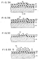
- a substrate 40 applied to the present invention is made of a transparent and electrically insulative material, e.g., glass material.
- a metal thin-film 42 having a predetermined pattern.
- the thin-film 42 is made, for example, of aluminum and is covered on the substrate 40 to include a thickness of approx. 1,000 A.
- the At thin-film 42 is formed by the known exposure techniques and etching techniques.
- an insulating thin-film 44 made of an electrically insulative material such as silicon dioxide, for example, by sputtering.
- an electrically insulative material such as silicon dioxide
- a conductive thin-film 46 having a predetermined thickness such as preferably approx. 2,000 A and made of a transparent and electrically conductive material.
- a negative photoresist material is further coated to maintain a predetermined thickness such as approx. 1.5 ⁇ m thick to form a negative photoresist film 48.
- a light such as ultraviolet ray 50 is illuminated to the structure of Fig. 3A from the bottom surface side of the transparent substrate 40. Accordingly, the negative photoresist film 48 is exposed with the light 50 with the metal thin-film 42 formed on the top surface of the substrate 40 as a mask pattern. Thereafter, when the above-mentioned structure is developed, the part exposed with the above-mentioned ultraviolet beam 50 through the transparent substrate 40, insulating film 44 and transparent conductive thin-film 46 of the negative photoresist film 48 is polymerized to become non-soluble in a solvent, and accordingly remains on the thin-film 46 as a resist pattern 48a as shown in Fig. 38.
- the part interrupted from the ultraviolet ray 50 by the metal thin-film 42 of the negative photoresist film 48 is dissolved in a solvent to form an opening 52 as shown in Fig. 3B.
- the shape of the opening 52 is precisely corresponded to the profile of the metal thin-film 42.
- the semiconductive thin-film made of polycrystalline or amorphous semiconductor material in this embodiment is deposited by a glow discharge decomposition method of SiH 4 , for example.
- the semiconductive thin-film is deposited on the top surface of the substrate of Fig. 3C to have a predetermined thickness, preferably approx. 6,000 A.
- the above-mentioned structure having the semiconductive thin-film is patterned by the known PEP technique to form a semiconductive thin-film 54 as shown in Fig. 3D.
- a wiring pattern is formed by the known method to complete the TFT 56.
- the metal thin-film 42 corresponds to the gate electrode of the TFT 56
- the transparent conductive thin-film 46a has portions 58 and 59 respectively corresponding to the source and drain electrodes of the TFT 56.
- the TFT 57 which can effectively prevent the source and drain electrodes 58 and 59 of the TFT 56 from extending in the approaching direction to one another to overlap the underlying gate electrode 42 above the gate electrode 42, can be manufactured.
- the TFT 56 in which the source and drain electrodes 58 and 59 accurately self-align with the gate electrode 42 can be manufactured.
- the elimination of the overlapping of the source and drain electrodes 58 and 59 with the gate electrode 42 causes to minimize the storage or parasitic capacitance of the transistor structure. Therefore, the upper limit of the operation frequency of the thin-film circuit including a plurality of TFTs can be enlarged and improved as well as the operating speed can be improved.
- the negative photoresist material for the photoresist film 48 should be selected.
- the resist pattern 48a remains on the necessary regions to become thereafter the source and drain electrodes 58 and 59 of the transparent conductive thin-film 46. Therefore, the lift-off method or lift-away method is not necessary to form the source and drain electrodes 58 and 59 by removing the unnecessary region part of the conductive thin-film 46. It is therefore essentially necessary to determine the thickness of a resist film and metal film and to set any particulars of the resist film, both of which are important in the lift-off method. Accordingly, the TFTs having the above-mentioned effective characteristics can be manufactured readily with good yield, and the microminiaturization of the TFTs can be accelerated. Therefore, the integration of the thin-film circuit including such the TFTs can be improved.
- a metal thin-film 42 functioning as a gate electrode is formed on a glass substrate or layer 40, an insulating thin-film 44 made of silicon dioxide is then deposited in a predetermined thickness, e.g., 3,000 A. Further, on the insulating thin-film 44 is deposited by sputtering a thin-film 60 which is made of a transparent and electrically conductive material such as indium-tin-oxide (ITO) in a predetermined thickness, e.g., preferably approx. 1,000 A thick.
- ITO indium-tin-oxide
- the amorphous silicon thin-film 62 is formed in a thickness of approx. 30 to 1,000 A, preferably approx. 200 A thickness.
- a negative photoresist material e.g., a negative resist "OMR-83" manufactured and sold by Tokyo Ohka Industrial Company, Tokyo, Japan
- a predetermined thickness e.g., approx. 0.5 ⁇ m on the top surface of the above-mentioned structure to provide a negative photoresist film 64.
- a light 50 e.g., ultraviolet ray is irradiated to the structure of Fig. 4A from the bottom surface side of the transparent substrate 40. Therefore, the negative photoresist film 64 is exposed with the light 50 through the substrate 40, insulating thin-film 44, ITO film 60 and thin-film 62 with the metal thin-film 42 formed on the substrate 40 as a mask pattern.
- the portion which is not exposed with the light 50 of the negative photoresist film 64 is removed to form a negative resist pattern 64a.
- the resist pattern 64a as a mask the amorphous silicon thin-film 62 to which phosphorus is doped and the ITO thin-film 60 are etched. This etched state is shown in Fig. 4B. At this time an opening 66 having a shape corresponding to the profile of the metal thin-film 42 is formed at the thin-films 60a and 62a thus etched.
- the remaining negative photoresist film 64a is removed by the known method from the structure of Fig. 4B.
- One portion 68 of the remaining thin-films 60a and 62a confronting each other through the opening 66 is used, for example, as a source electrode, and the other portion 70 is used as a drain electrode.
- the amorphous silicon film On the top surface including the opening 66 of the structure of Fig. 4C is deposited the amorphous silicon film in a predetermined thickness, e.g., 5,000 A thick, for example, by a glow discharge decomposition method of SiH 4 .
- This amorphous silicon film is patterned by the known PEP technique to form a semiconductive thin-film 72 as shown in Fig. 4D. Since the following manufacturing process is similar to the known process, the description of the process will be omitted. In this manner the TFT 74 is manufactured.
- the amorphous silicon thin-film 62a including low resistance is formed on the top surfaces of the source and drain electrodes 68 and 70 and hence on the ITO film 60a. Accordingly, the ohmic contact of the ITO film 60a with the semiconductive thin-film 72 functioning as the channel of the TFT 74 having electrically bad junction to one another can be improved. Further, since the negative photoresist 64 is coated after the deposition of the low resistive semiconductive film 62 added with an impurity in the method for manufacturing according to the above-mentioned embodiment disclosed with reference to Figs.
- the yield of manufacturing the TFTs can be improved.
- another method e.g., a method of lifting off the low resistive thin-film deposited by a known CVD process after the formation of the positive photoresist pattern can be considered.
- the other method which employs such the lift-off method there are problems such as those in which the photoresist material is undesirably hardened due to the generated heat, the low resistive semiconductive thin-film is contaminated and/or the characteristic is deteriorated.
- the thin-film circuit including a number of TFTs can be readily manufactured in high yield and high integration.
- the thickness of the low resistive amorphous silicon thin-film 62 is selected to approx. 30 to 1,000 A as described above in Fig. 4A, but this is for the purpose of obtaining preferable ohmic contact.
- the amorphous silicon thin-film 62 including the thickness of the above-mentioned numeral value has a transmittance which can practically satisfy for the light 50.
- the spectral sensitivity range of the negative photoresist film 64 for the incident light is ordinarily known to be less than approx.
- the negative photoresist film 64 could be sensitized in the sufficiently satisfactory contrast by using the amorphous silicon thin-film 62 including the above-mentioned thickness. Therefore, the source and drain electrodes 68 and 70 of the TFT 74 could be accurately self-aligned with the underlying gate electrode 42 and formed.
- the amorphous semiconductor material used in the method for manufacturing the TFTs of the present invention is not limited only to the silicon applied in the above-mentioned embodiments, but other substances such as, for example, semiconductor compound, e.g., germanium (Ge) or Ge x Si l - x , Si x C l - x , etc. may be used.
- semiconductor compound e.g., germanium (Ge) or Ge x Si l - x , Si x C l - x , etc.
- the materials used in the above-mentioned embodiments illustrate only by way of examples, but may be altered in response to the state of the manufacture.
- the gate insulating film 44 is not limited only to the silicon dioxide (Si0 2 ), but other material such as Si 3 N 4 may be used.
- the gate electrode 42 may be any of electrically conductive material having opaque property for the incident radiation, e.g., the light 50.
- indium-oxide or tin-oxide may be used for ITO as material of which the transparent thin-film 60 is formed on the insulating thin-film 44.
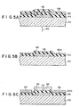
- the source and drain electrodes 68 and 70 of the TFT 74 are manufactured to include the laminar structure, but are not limited only this, but may be constructed as in the modified embodiment shown, for example, in Figs. 5A to 5C.
- the low resistive amorphous semiconductive thin-film 80 is deposited directly on the gate insulating film 44 deposited on the top surface of the structure made of a substrate 40 and a gate electrode 42.
- a negative photoresist film 64 is provided as described above.
- amorphous semiconductive thin-film 80a thus etched is self-aligned with the gate electrode 42 on the same reason as that described with reference to the above-mentioned embodiments.
- electrically conductive thin-films 84 and 86 are formed together with an amorphous semiconductive thin-film 88 functioning as the channel unit.
- the conductive thin-films 84 and 86 are formed on the above-mentioned low resistive thin-film 80a.
- the conductive thin-films 84 and 86 are made, for example, of conductive material, e.g., molybdenum, indium or tin oxide.
- the conductive thin-films 84 and 86 are not contacted with or formed in junction with the channel thin-film 88 directly.
- the channel thin-film 88 is formed on the predetermined surface region including the opening 82 of the structure of Fig. 5B, and is partly overlaid on the low resistive thin-film 80a. In this manner, the above-mentioned conductive thin-films 84 and 86 are electrically connected only through the low resistive thin-film 80a.
- the conductive films 84 and 86 are conplementarily used as the source and drain electrodes and mainly contain low resistive thin-film 80a.
Landscapes
- Thin Film Transistor (AREA)
Applications Claiming Priority (4)
| Application Number | Priority Date | Filing Date | Title |
|---|---|---|---|
| JP56117423A JPS5818966A (ja) | 1981-07-27 | 1981-07-27 | 薄膜電界効果トランジスタの製造方法 |
| JP117423/81 | 1981-07-27 | ||
| JP51421/82 | 1982-03-31 | ||
| JP57051421A JPS58170065A (ja) | 1982-03-31 | 1982-03-31 | 薄膜電界効果トランジスタの製造方法 |
Publications (3)
| Publication Number | Publication Date |
|---|---|
| EP0071244A2 true EP0071244A2 (de) | 1983-02-09 |
| EP0071244A3 EP0071244A3 (en) | 1985-05-15 |
| EP0071244B1 EP0071244B1 (de) | 1988-11-23 |
Family
ID=26391952
Family Applications (1)
| Application Number | Title | Priority Date | Filing Date |
|---|---|---|---|
| EP82106781A Expired EP0071244B1 (de) | 1981-07-27 | 1982-07-27 | Dünnschichttransistor und Verfahren zu dessen Herstellung |
Country Status (3)
| Country | Link |
|---|---|
| US (1) | US4700458A (de) |
| EP (1) | EP0071244B1 (de) |
| DE (1) | DE3279239D1 (de) |
Cited By (11)
| Publication number | Priority date | Publication date | Assignee | Title |
|---|---|---|---|---|
| GB2134707A (en) * | 1982-12-29 | 1984-08-15 | Sharp Kk | Thin film transistor with laminated source and drain electrodes and method of manufacture |
| FR2548450A1 (fr) * | 1983-06-29 | 1985-01-04 | Citizen Watch Co Ltd | Procede de fabrication de diode en film mince ultra-miniature |
| US4678542A (en) * | 1986-07-25 | 1987-07-07 | Energy Conversion Devices, Inc. | Self-alignment process for thin film diode array fabrication |
| EP0196915A3 (en) * | 1985-03-29 | 1987-12-02 | Matsushita Electric Industrial Co., Ltd. | Thin film transistor array and method of manufacturing same |
| US4797108A (en) * | 1984-03-10 | 1989-01-10 | Lucas Industries Public Limited Company | Method of manufacturing amorphous silicon field effect transistors |
| EP0308128A1 (de) * | 1987-09-09 | 1989-03-22 | Btg International Limited | Verfahren zur Herstellung von Dünnschicht Transistoren |
| EP0416798A3 (en) * | 1989-09-04 | 1991-06-05 | Canon Kabushiki Kaisha | Manufacturing method for semiconductor device |
| US5045487A (en) * | 1982-03-31 | 1991-09-03 | Fujitsu Limited | Process for producing a thin film field-effect transistor |
| EP0493113A3 (en) * | 1990-12-28 | 1992-09-02 | Sharp Kabushiki Kaisha | A method for producing an active matrix substrate for liquid crystal display devices |
| EP0516335A3 (en) * | 1991-05-31 | 1993-09-08 | American Telephone And Telegraph Company | Fabrication method in vertical transistor integration |
| US5474941A (en) * | 1990-12-28 | 1995-12-12 | Sharp Kabushiki Kaisha | Method for producing an active matrix substrate |
Families Citing this family (37)
| Publication number | Priority date | Publication date | Assignee | Title |
|---|---|---|---|---|
| US6784033B1 (en) * | 1984-02-15 | 2004-08-31 | Semiconductor Energy Laboratory Co., Ltd. | Method for the manufacture of an insulated gate field effect semiconductor device |
| US5166086A (en) * | 1985-03-29 | 1992-11-24 | Matsushita Electric Industrial Co., Ltd. | Thin film transistor array and method of manufacturing same |
| JPS62291067A (ja) * | 1986-06-10 | 1987-12-17 | Nec Corp | 薄膜トランジスタの製造方法 |
| US5198377A (en) * | 1987-07-31 | 1993-03-30 | Kinya Kato | Method of manufacturing an active matrix cell |
| US4767723A (en) * | 1987-10-30 | 1988-08-30 | International Business Machines Corporation | Process for making self-aligning thin film transistors |
| US4960719A (en) * | 1988-02-04 | 1990-10-02 | Seikosha Co., Ltd. | Method for producing amorphous silicon thin film transistor array substrate |
| GB2220792B (en) * | 1988-07-13 | 1991-12-18 | Seikosha Kk | Silicon thin film transistor and method for producing the same |
| JP2862571B2 (ja) * | 1988-07-28 | 1999-03-03 | 株式会社東芝 | 透過型液晶表示装置 |
| JPH0283941A (ja) * | 1988-09-21 | 1990-03-26 | Fuji Xerox Co Ltd | 薄膜トランジスタの製造方法 |
| GB2223353A (en) * | 1988-09-30 | 1990-04-04 | Philips Electronic Associated | Thin-film transistor |
| US5042918A (en) * | 1988-11-15 | 1991-08-27 | Kabushiki Kaisha Toshiba | Liquid crystal display device |
| US5204276A (en) * | 1988-12-06 | 1993-04-20 | Kabushiki Kaisha Toshiba | Method of manufacturing semiconductor device |
| US5132745A (en) * | 1990-10-05 | 1992-07-21 | General Electric Company | Thin film transistor having an improved gate structure and gate coverage by the gate dielectric |
| US5156986A (en) * | 1990-10-05 | 1992-10-20 | General Electric Company | Positive control of the source/drain-gate overlap in self-aligned TFTS via a top hat gate electrode configuration |
| US5198694A (en) * | 1990-10-05 | 1993-03-30 | General Electric Company | Thin film transistor structure with improved source/drain contacts |
| JPH04505830A (ja) * | 1990-10-05 | 1992-10-08 | ゼネラル・エレクトリック・カンパニイ | トップハット形ゲート電極形式によるセルフアラインtftにおけるソース/ドレイン―ゲートの重なりの確実な制御 |
| JPH07506703A (ja) * | 1993-03-01 | 1995-07-20 | ゼネラル・エレクトリック・カンパニイ | 持ち上げ方法を用いて構成されたセルフアライン薄膜トランジスタ |
| KR0135391B1 (ko) * | 1994-05-28 | 1998-04-22 | 김광호 | 자기정렬된 액정표시장치용 박막트랜지스터 및 제조방법 |
| JP3478012B2 (ja) * | 1995-09-29 | 2003-12-10 | ソニー株式会社 | 薄膜半導体装置の製造方法 |
| US5986391A (en) * | 1998-03-09 | 1999-11-16 | Feldman Technology Corporation | Transparent electrodes |
| GB9919913D0 (en) * | 1999-08-24 | 1999-10-27 | Koninkl Philips Electronics Nv | Thin-film transistors and method for producing the same |
| JP4247377B2 (ja) * | 2001-12-28 | 2009-04-02 | 独立行政法人産業技術総合研究所 | 薄膜トランジスタ及びその製造方法 |
| US7067439B2 (en) | 2002-06-14 | 2006-06-27 | Applied Materials, Inc. | ALD metal oxide deposition process using direct oxidation |
| TWI236153B (en) * | 2004-01-05 | 2005-07-11 | Quanta Display Inc | Method for fabricating self-aligned TFT |
| US8119210B2 (en) | 2004-05-21 | 2012-02-21 | Applied Materials, Inc. | Formation of a silicon oxynitride layer on a high-k dielectric material |
| US20060105114A1 (en) * | 2004-11-16 | 2006-05-18 | White John M | Multi-layer high quality gate dielectric for low-temperature poly-silicon TFTs |
| US20060199314A1 (en) * | 2005-03-02 | 2006-09-07 | Chiun-Hung Chen | Thin film transistor, and method of fabricating thin film transistor and pixel structure |
| US7645710B2 (en) | 2006-03-09 | 2010-01-12 | Applied Materials, Inc. | Method and apparatus for fabricating a high dielectric constant transistor gate using a low energy plasma system |
| US7837838B2 (en) | 2006-03-09 | 2010-11-23 | Applied Materials, Inc. | Method of fabricating a high dielectric constant transistor gate using a low energy plasma apparatus |
| US7678710B2 (en) | 2006-03-09 | 2010-03-16 | Applied Materials, Inc. | Method and apparatus for fabricating a high dielectric constant transistor gate using a low energy plasma system |
| TWI435376B (zh) | 2006-09-26 | 2014-04-21 | 應用材料股份有限公司 | 用於缺陷鈍化之高k閘極堆疊的氟電漿處理 |
| WO2011129227A1 (ja) | 2010-04-14 | 2011-10-20 | シャープ株式会社 | 半導体装置、半導体装置の製造方法、および表示装置 |
| US9171840B2 (en) * | 2011-05-26 | 2015-10-27 | Semiconductor Energy Laboratory Co., Ltd. | Semiconductor device and manufacturing method thereof |
| FR2998580B1 (fr) * | 2012-11-26 | 2016-10-21 | Institut De Rech Pour Le Developpement Ird | Marqueurs moleculaires et methodes pour l'identification des genotypes de palmier dattier |
| CN104040683B (zh) * | 2012-11-30 | 2017-04-19 | 深圳市柔宇科技有限公司 | 自对准金属氧化物薄膜晶体管器件及制造方法 |
| CN112242441A (zh) * | 2019-07-16 | 2021-01-19 | 联华电子股份有限公司 | 高电子迁移率晶体管 |
| CN115483277A (zh) * | 2022-09-30 | 2022-12-16 | 惠科股份有限公司 | 薄膜晶体管、显示面板及其制备方法 |
Family Cites Families (8)
| Publication number | Priority date | Publication date | Assignee | Title |
|---|---|---|---|---|
| DE1071576B (de) * | 1959-12-17 | Maria Josephus Antonius Dassen, Antonius Lodewijk Josephus Marie Dassen, Lodewijk Arnoldus Franciscus Mar'ia Dassen, Eindhoven und Arnold Modeste Marie Dassen, Waalre (Niederlande) | Verpackungsschachtdl, insbesondere für die Verpakk'umg von Zigarren | |
| NL294370A (de) * | 1963-06-20 | |||
| US4049963A (en) * | 1973-09-14 | 1977-09-20 | Coulter Information Systems, Inc. | Photoelectric measuring device |
| US4065781A (en) * | 1974-06-21 | 1977-12-27 | Westinghouse Electric Corporation | Insulated-gate thin film transistor with low leakage current |
| US4174217A (en) * | 1974-08-02 | 1979-11-13 | Rca Corporation | Method for making semiconductor structure |
| US4393572A (en) * | 1980-05-29 | 1983-07-19 | Rca Corporation | Method of making low leakage N-channel SOS transistors utilizing positive photoresist masking techniques |
| US4459739A (en) * | 1981-05-26 | 1984-07-17 | Northern Telecom Limited | Thin film transistors |
| JPS58170067A (ja) * | 1982-03-31 | 1983-10-06 | Fujitsu Ltd | 薄膜トランジスタの製造方法 |
-
1982
- 1982-07-27 EP EP82106781A patent/EP0071244B1/de not_active Expired
- 1982-07-27 DE DE8282106781T patent/DE3279239D1/de not_active Expired
-
1985
- 1985-09-24 US US06/779,648 patent/US4700458A/en not_active Expired - Lifetime
Cited By (14)
| Publication number | Priority date | Publication date | Assignee | Title |
|---|---|---|---|---|
| US5045487A (en) * | 1982-03-31 | 1991-09-03 | Fujitsu Limited | Process for producing a thin film field-effect transistor |
| GB2134707A (en) * | 1982-12-29 | 1984-08-15 | Sharp Kk | Thin film transistor with laminated source and drain electrodes and method of manufacture |
| FR2548450A1 (fr) * | 1983-06-29 | 1985-01-04 | Citizen Watch Co Ltd | Procede de fabrication de diode en film mince ultra-miniature |
| US4797108A (en) * | 1984-03-10 | 1989-01-10 | Lucas Industries Public Limited Company | Method of manufacturing amorphous silicon field effect transistors |
| EP0196915A3 (en) * | 1985-03-29 | 1987-12-02 | Matsushita Electric Industrial Co., Ltd. | Thin film transistor array and method of manufacturing same |
| US4678542A (en) * | 1986-07-25 | 1987-07-07 | Energy Conversion Devices, Inc. | Self-alignment process for thin film diode array fabrication |
| US4968638A (en) * | 1987-09-09 | 1990-11-06 | National Research Development Corporation | Semiconductor devices |
| EP0308128A1 (de) * | 1987-09-09 | 1989-03-22 | Btg International Limited | Verfahren zur Herstellung von Dünnschicht Transistoren |
| EP0416798A3 (en) * | 1989-09-04 | 1991-06-05 | Canon Kabushiki Kaisha | Manufacturing method for semiconductor device |
| US5656511A (en) * | 1989-09-04 | 1997-08-12 | Canon Kabushiki Kaisha | Manufacturing method for semiconductor device |
| EP0493113A3 (en) * | 1990-12-28 | 1992-09-02 | Sharp Kabushiki Kaisha | A method for producing an active matrix substrate for liquid crystal display devices |
| US5286659A (en) * | 1990-12-28 | 1994-02-15 | Sharp Kabushiki Kaisha | Method for producing an active matrix substrate |
| US5474941A (en) * | 1990-12-28 | 1995-12-12 | Sharp Kabushiki Kaisha | Method for producing an active matrix substrate |
| EP0516335A3 (en) * | 1991-05-31 | 1993-09-08 | American Telephone And Telegraph Company | Fabrication method in vertical transistor integration |
Also Published As
| Publication number | Publication date |
|---|---|
| US4700458A (en) | 1987-10-20 |
| DE3279239D1 (en) | 1988-12-29 |
| EP0071244A3 (en) | 1985-05-15 |
| EP0071244B1 (de) | 1988-11-23 |
Similar Documents
| Publication | Publication Date | Title |
|---|---|---|
| US4700458A (en) | Method of manufacture thin film transistor | |
| US4958205A (en) | Thin film transistor array and method of manufacturing the same | |
| KR100485531B1 (ko) | 다결정 실리콘 박막트랜지스터와 그 제조방법 | |
| US5010027A (en) | Method for fabricating a self-aligned thin-film transistor utilizing planarization and back-side photoresist exposure | |
| EP0304657B1 (de) | Aktive Matrixzelle und deren Herstellungsverfahren | |
| US6329672B1 (en) | Thin film transistor having a second gate metal layer preventing formation of hillocks | |
| US5391507A (en) | Lift-off fabrication method for self-aligned thin film transistors | |
| KR20000027712A (ko) | 액정 표시 장치용 박막 트랜지스터 기판의 제조 방법 | |
| US5751020A (en) | Structure of a liquid crystal display unit having exposed channel region | |
| US5166086A (en) | Thin film transistor array and method of manufacturing same | |
| US6100950A (en) | Active matrix LCD with thin film transistor switches and method of producing the same | |
| KR20010110139A (ko) | 개량된 프로세스 윈도우를 구비한 완전 셀프-얼라인된tft를 형성하는 방법 | |
| US4599246A (en) | Method of producing liquid-crystal display device | |
| KR100590750B1 (ko) | 액정표시장치용박막트랜지스터기판의제조방법 | |
| JP2678044B2 (ja) | アクティブマトリクス基板の製造方法 | |
| US6043113A (en) | Method of forming self-aligned thin film transistor | |
| EP0519692A2 (de) | Dünnfilmtransistor und Verfahren zu dessen Herstellung | |
| JPH06101478B2 (ja) | 薄膜トランジスタとその製造方法 | |
| JP3238072B2 (ja) | 薄膜トランジスタ | |
| JP3340782B2 (ja) | 薄膜半導体素子 | |
| JP3419073B2 (ja) | 薄膜トランジスタ及びその製造方法、及びアクティブマトリクス液晶表示素子 | |
| JPH059940B2 (de) | ||
| JPH01236655A (ja) | 薄膜電界効果トランジスタとその製造方法 | |
| JP3097229B2 (ja) | 薄膜トランジスタ素子アレイとその製造方法 | |
| JPH08204200A (ja) | 薄膜トランジスタ |
Legal Events
| Date | Code | Title | Description |
|---|---|---|---|
| PUAI | Public reference made under article 153(3) epc to a published international application that has entered the european phase |
Free format text: ORIGINAL CODE: 0009012 |
|
| 17P | Request for examination filed |
Effective date: 19820727 |
|
| AK | Designated contracting states |
Designated state(s): DE FR GB |
|
| RAP1 | Party data changed (applicant data changed or rights of an application transferred) |
Owner name: KABUSHIKI KAISHA TOSHIBA |
|
| PUAL | Search report despatched |
Free format text: ORIGINAL CODE: 0009013 |
|
| AK | Designated contracting states |
Designated state(s): DE FR GB |
|
| 17Q | First examination report despatched |
Effective date: 19860409 |
|
| GRAA | (expected) grant |
Free format text: ORIGINAL CODE: 0009210 |
|
| AK | Designated contracting states |
Kind code of ref document: B1 Designated state(s): DE FR GB |
|
| REF | Corresponds to: |
Ref document number: 3279239 Country of ref document: DE Date of ref document: 19881229 |
|
| ET | Fr: translation filed | ||
| PLBE | No opposition filed within time limit |
Free format text: ORIGINAL CODE: 0009261 |
|
| STAA | Information on the status of an ep patent application or granted ep patent |
Free format text: STATUS: NO OPPOSITION FILED WITHIN TIME LIMIT |
|
| 26N | No opposition filed | ||
| REG | Reference to a national code |
Ref country code: GB Ref legal event code: 746 Effective date: 19990216 |
|
| REG | Reference to a national code |
Ref country code: FR Ref legal event code: D6 |
|
| PGFP | Annual fee paid to national office [announced via postgrant information from national office to epo] |
Ref country code: FR Payment date: 20010712 Year of fee payment: 20 |
|
| PGFP | Annual fee paid to national office [announced via postgrant information from national office to epo] |
Ref country code: DE Payment date: 20010723 Year of fee payment: 20 |
|
| PGFP | Annual fee paid to national office [announced via postgrant information from national office to epo] |
Ref country code: GB Payment date: 20010725 Year of fee payment: 20 |
|
| REG | Reference to a national code |
Ref country code: GB Ref legal event code: IF02 |
|
| PG25 | Lapsed in a contracting state [announced via postgrant information from national office to epo] |
Ref country code: GB Free format text: LAPSE BECAUSE OF EXPIRATION OF PROTECTION Effective date: 20020726 |
|
| REG | Reference to a national code |
Ref country code: GB Ref legal event code: PE20 Effective date: 20020726 |