EP0311109A2 - Méthode de fabrication d'un transistor à effet de champ à porte à jonction - Google Patents
Méthode de fabrication d'un transistor à effet de champ à porte à jonction Download PDFInfo
- Publication number
- EP0311109A2 EP0311109A2 EP88116670A EP88116670A EP0311109A2 EP 0311109 A2 EP0311109 A2 EP 0311109A2 EP 88116670 A EP88116670 A EP 88116670A EP 88116670 A EP88116670 A EP 88116670A EP 0311109 A2 EP0311109 A2 EP 0311109A2
- Authority
- EP
- European Patent Office
- Prior art keywords
- layer
- insulating film
- forming
- ion
- opening portion
- Prior art date
- Legal status (The legal status is an assumption and is not a legal conclusion. Google has not performed a legal analysis and makes no representation as to the accuracy of the status listed.)
- Granted
Links
Images


Classifications
-
- H—ELECTRICITY
- H10—SEMICONDUCTOR DEVICES; ELECTRIC SOLID-STATE DEVICES NOT OTHERWISE PROVIDED FOR
- H10D—INORGANIC ELECTRIC SEMICONDUCTOR DEVICES
- H10D30/00—Field-effect transistors [FET]
- H10D30/01—Manufacture or treatment
- H10D30/051—Manufacture or treatment of FETs having PN junction gates
-
- H—ELECTRICITY
- H10—SEMICONDUCTOR DEVICES; ELECTRIC SOLID-STATE DEVICES NOT OTHERWISE PROVIDED FOR
- H10D—INORGANIC ELECTRIC SEMICONDUCTOR DEVICES
- H10D30/00—Field-effect transistors [FET]
- H10D30/80—FETs having rectifying junction gate electrodes
- H10D30/83—FETs having PN junction gate electrodes
-
- H—ELECTRICITY
- H10—SEMICONDUCTOR DEVICES; ELECTRIC SOLID-STATE DEVICES NOT OTHERWISE PROVIDED FOR
- H10D—INORGANIC ELECTRIC SEMICONDUCTOR DEVICES
- H10D62/00—Semiconductor bodies, or regions thereof, of devices having potential barriers
- H10D62/10—Shapes, relative sizes or dispositions of the regions of the semiconductor bodies; Shapes of the semiconductor bodies
- H10D62/17—Semiconductor regions connected to electrodes not carrying current to be rectified, amplified or switched, e.g. channel regions
- H10D62/351—Substrate regions of field-effect devices
-
- H—ELECTRICITY
- H10—SEMICONDUCTOR DEVICES; ELECTRIC SOLID-STATE DEVICES NOT OTHERWISE PROVIDED FOR
- H10D—INORGANIC ELECTRIC SEMICONDUCTOR DEVICES
- H10D62/00—Semiconductor bodies, or regions thereof, of devices having potential barriers
- H10D62/80—Semiconductor bodies, or regions thereof, of devices having potential barriers characterised by the materials
- H10D62/85—Semiconductor bodies, or regions thereof, of devices having potential barriers characterised by the materials being Group III-V materials, e.g. GaAs
-
- Y—GENERAL TAGGING OF NEW TECHNOLOGICAL DEVELOPMENTS; GENERAL TAGGING OF CROSS-SECTIONAL TECHNOLOGIES SPANNING OVER SEVERAL SECTIONS OF THE IPC; TECHNICAL SUBJECTS COVERED BY FORMER USPC CROSS-REFERENCE ART COLLECTIONS [XRACs] AND DIGESTS
- Y10—TECHNICAL SUBJECTS COVERED BY FORMER USPC
- Y10S—TECHNICAL SUBJECTS COVERED BY FORMER USPC CROSS-REFERENCE ART COLLECTIONS [XRACs] AND DIGESTS
- Y10S148/00—Metal treatment
- Y10S148/088—J-Fet, i.e. junction field effect transistor
-
- Y—GENERAL TAGGING OF NEW TECHNOLOGICAL DEVELOPMENTS; GENERAL TAGGING OF CROSS-SECTIONAL TECHNOLOGIES SPANNING OVER SEVERAL SECTIONS OF THE IPC; TECHNICAL SUBJECTS COVERED BY FORMER USPC CROSS-REFERENCE ART COLLECTIONS [XRACs] AND DIGESTS
- Y10—TECHNICAL SUBJECTS COVERED BY FORMER USPC
- Y10S—TECHNICAL SUBJECTS COVERED BY FORMER USPC CROSS-REFERENCE ART COLLECTIONS [XRACs] AND DIGESTS
- Y10S148/00—Metal treatment
- Y10S148/10—Lift-off masking
-
- Y—GENERAL TAGGING OF NEW TECHNOLOGICAL DEVELOPMENTS; GENERAL TAGGING OF CROSS-SECTIONAL TECHNOLOGIES SPANNING OVER SEVERAL SECTIONS OF THE IPC; TECHNICAL SUBJECTS COVERED BY FORMER USPC CROSS-REFERENCE ART COLLECTIONS [XRACs] AND DIGESTS
- Y10—TECHNICAL SUBJECTS COVERED BY FORMER USPC
- Y10S—TECHNICAL SUBJECTS COVERED BY FORMER USPC CROSS-REFERENCE ART COLLECTIONS [XRACs] AND DIGESTS
- Y10S148/00—Metal treatment
- Y10S148/105—Masks, metal
Definitions
- the present invention relates to a method of manufacturing a junction type field effect semiconductor device using a III - V Group compound semiconductor substrate.
- GaAsFET GaAs field effect transistor
- MES metal semiconductor
- J-FET junction type
- junction barrier height ⁇ B of the J-FET is as high as 1 V or more. Therefore, a sufficient operation margin can be obtained for a normally-off type J-FET.
- a complementary circuit can be arranged.
- the type of J-FET varies in accordance with a formation type of a gate region. That is, the J-FET has a variety of types such as a diffusion junction type, an ion-implantation junction type, and an epitaxial growth junction type. In any of the above types, however, it is difficult to perform micropatterning of a gate portion as compared with the MES type, and a micropatterning technique for the J-FET has not been developed yet. That is, in a conventional technique, a gate region is formed in a semiconductor substrate, and then a gate electrode is positioned on the gate region by mask alignment. Thereafter, the gate electrode is formed by a lift-off method or etching.
- the gate electrode is formed not directly on the gate region but on a region electrically connected to the gate region.
- the gate region is a small region. This is because mutual conductance gm as a performance factor of a semiconductor device is proportional to W (channel width)/L (channel length) and therefore W must be increased and L must be decreased in order to increase the value of gm. Since the gate region is a small region, it is very difficult for current techniques to stably position the gate electrode on the small region with high accuracy by mask alignment, resulting in a very poor yield. In addition, when the gate electrode is formed on the region electrically connected to the gate region, a gate resistance is increased by a resistance of this region. For this reason, as an operation frequency is increased, a noise factor (NF) is increased and a gain is reduced. Therefore, this method is not preferable as a method of manufacturing a gate portion of a high frequency FET.
- NF noise factor
- the manufacturing yield is very poor.
- a high frequency performance is degraded.
- the present invention has been made in consideration of the above situation and has as its object to provide a method of manufacturing a semiconductor device, which can stably position a gate electrode with respect to a small gate region with high accuracy and can manufacture a semiconductor device suitable for high frequency applications.
- a method of manufacturing a semiconductor device comprising the steps of: implanting ions of impurity Si in compound semiconductor substrate and forming a first ion-implantation layer of a first conductivity type on a major surface layer of the substrate; forming first insulating film on the major surface of the substrate; forming second insulating film having opening portion on the first insulating film; forming opening portion in the first insulating film by selective etching using the second insulating film as a mask; implanting ions of impurity in the first ion-implantation layer through the opening portion of the second insulating film and forming second ion-implantation layer of a second conductivity type in a surface layer thereof; forming, on the major surface of the structure, while the second insulating film remains, conductor layers in which at least a layer thereof contacting the semiconductor substrate is either a refractory metal layer or a layer containing a refractory metal; removing the second insulating film to remove conductor layer
- a method of manufacturing a semiconductor device comprising the steps of: forming semiconductor layer of a first conductivity type on compound semiconductor substrate; forming insulating film having an opening portion on a major surface of the semiconductor layer; forming groove in the semiconductor layer by selective etching using the insulating film as a mask; implanting impurity ions in the semiconductor layer through the opening portion of the insulating film and the groove of the semiconductor layer and forming ion-implantation layer of a second conductivity type in a major surface layer of the semiconductor layer exposed in the groove; forming, on a major surface of a structure, while the insulating film remains, conductor layers in which at least a layer thereof contacting the semiconductor layer is either a refractory metal layer or a layer containing a refractory metal; removing the insulating film to remove conductor layer portion formed thereon, thereby forming electrode so that only conductor layer portion exposed in the opening portion of the
- the insulating film used as a mask during ion-implantation for forming the gate region can be used as a mask for sputtering the gate electrode material. Therefore, the gate electrode can be formed in self-alignment with the gate region.
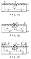
- Figs. 1A to 1F are sectional views showing the structures of the device formed in manufacturing steps according to an embodiment in which the present invention is applied to a method of manufacturing an ion-implantation J-FET (junction type field effect transistor).
- J-FET junction type field effect transistor
- Si is selectively ion-implanted in a major surface of GaAs substrate 10.
- ion-implantation is performed in prospective source and drain formation regions under conditions that acceleration voltage V ac is 180 KeV and dosage Q d is 5 ⁇ 1013/cm2, thereby forming ion-implantation layers 11 and 12.
- ion-implantation is performed in a prospective channel formation region under conditions that acceleration voltage V ac is 100 KeV and dosage Q d is 3 ⁇ 1012/cm2, thereby forming ion-implantation layer 13.
- SiO2 film 14 is formed on the entire major surface of substrate 10 to have a thickness of 5,000 ⁇ by CVD (chemical vapor deposition), and photoresist film 16 having opening portion 15 at a position corresponding to a gate region is formed on SiO2 film 14. Subsequently, film 14 is etched by an isotropic etching technique using film 16 as a mask and an NH4F solution, thereby forming opening portion 17 in film 14. Thereafter, Zn+ is ion-implanted in layer 13 through opening portions 15 and 17 under conditions that acceleration voltage V ac is 80 KeV and dosage Q d is 1 ⁇ 1015/cm2, thereby forming ion-implantation layer 18 in layer 13.
- CVD chemical vapor deposition
- Conductor layer 19 is formed on the entire major surface of the structure of the device.
- Conductor layer 19 comprises a 1,000- ⁇ thick lower TiW layer and a 5,000- ⁇ thick upper Au layer, which are formed in an Ar gas atmosphere by a sputtering process.
- the TiW layer is formed on film 16 and the Au layer is formed on the TiW layer.
- TiW and Au are sputtered on layer 13 through opening portion 15 of film 16 and opening portion 17 of film 14, thereby forming conductor layer 19A on layer 13.
- Materials other than TiW and Au may be used, as long as an ohmic contact between the layer formed of the materials and the gate region is not degraded, even when the layers are annealed in the following step.
- a single layer containing a refractory metal such as a WN layer or a WSi layer may be used.
- a bi-layered structure having a lower WN layer contacting GaAs substrate 10 and an upper Au layer may be used. That is, any kind of layer may be used in place of the above layer of this embodiment as long as the layer contacting substrate 10 is made of a refractory metal.
- layer 19 formed on film 16 is simultaneously removed. That is, layer 19 is removed by a so-called “lift off” method. As a result, only layer 19A remains formed on layer 13 to form gate electrode 20.
- PSG film 21 is formed by the CVD process on the entire major surface of the structure to have a thickness of 5,000 ⁇ . Thereafter, the structure is annealed for 15 minutes in an Ar gas at 800°C to activate the ion-implanted impurity, thereby forming N+-type source and drain regions 22 and 23, N-type channel region 24, and P-type gate region 25. By way of this annealing process, electrode 20 is formed in ohmic contact with region 25.
- Source and drain leading electrodes 26 and 27 each comprising a 2,000- ⁇ thick lower AuGe film containing 5% of Ge and a 1,000- ⁇ thick upper Au film are formed in the openings of film 21 by, e.g., a lift-off method. Thereafter, the structure is annealed at 400°C for three minutes to form an ohmic contact between source region 22 and source leading electrode 26 and an ohmic contact between drain region 23 and drain leading electrode 27. Following this annealing process, source and drain electrodes 28 and 29 are formed on source and drain leading electrodes 26 and 27, respectively, by, e.g., a lift-off method. Source and drain electrodes 28 and 29 may be a superposed structure composed of a Ti layer - Pt layer-Au layer. In this way, the J-FET is completed.
- gate electrode 20 is in direct contact with gate region 25. Therefore, a gate resistance can be sufficiently reduced, and a noise factor and a gain at a high frequency is not degraded.
- gate region 25 and gate electrode 20 are formed through opening portion 15 in photoresist film 16 by ion-implantation and sputtering, gate region 25 and gate electrode 20 are in self-alignment with each other. For this reason, even if region 25 is formed to occupy a small area, a positional deviation is not generated between region 25 and electrode 20, resulting in a high manufacturing yield.
- the structure is annealed to form source and drain regions 22 and 23 and channel and gate regions 24 and 25.
- the impurity in ion-implantation layer 18 is activated and gate region 25 is formed to extend in the lateral direction. Since region 25 extends in the lateral direction, there is almost no possibility of gate electrode 20 contacting channel region 24.
- Figs. 2A to 2G are sectional views of the structures formed in manufacturing steps according to another embodiment in which the present invention is applied to a method of manufacturing an ion-implantation J-FET (junction type field effect transistor).
- J-FET junction type field effect transistor
- Si is selectively ion-implanted in a major surface of GaAs substrate 10.
- ion-implantation is performed in prospective source and drain formation regions under conditions that acceleration voltage V ac is 180 KeV and dosage Q d is 5 ⁇ 1013/cm2, thereby forming ion-implantation layers 11 and 12.
- ion-implantation is performed in a prospective channel formation region under conditions that acceleration voltage V ac is 100 KeV and dosage Q d is 3 ⁇ 1012/cm2, thereby forming ion-implantation layer 13.
- SiO2 film 14 is formed by a CVD process (chemical vapor deposition) on the entire major surface of substrate 10 to have a thickness of 5,000 ⁇ , and photoresist film 16 having opening portion 15 at a position corresponding to a gate region is formed thereon. Subsequently, film 14 is etched by an isotropic etching technique using film 16 as a mask and an NH4F solution, thereby forming opening portion 17 in film 14. Thereafter, Zn+ is ion-implanted in layer 13 through opening portions 15 and 17 under conditions that acceleration voltage V ac is 80 KeV and dosage Q d is 1 ⁇ 1015/cm2, thereby forming ion-implantation layer 18 in layer 13.
- CVD process chemical vapor deposition
- Conductor layer 19 is formed on the entire major surface of the structure of the device.
- Conductor layer 19 comprises a 1,000- ⁇ thick lower TiW layer and a 5,000- ⁇ thick upper Au layer, which are formed in an Ar gas atmosphere by a sputtering technique.
- the TiW layer is formed on film 16 and the Au layer is formed on the TiW layer.
- TiW and Au are sputtered onto layer 13 through opening portion 15 of film 16 and through opening portion 17 of film 14, thereby forming conductor layer 19A on layer 13.
- Materials other than TiW and Au may be used, as long as an ohmic contact between the layer formed of the materials and the gate region is not degraded, even when the layers are annealed in the following step.
- a single layer containing a refractory metal such as a WN layer or a WSi layer may be used.
- a bi-layered structure of a lower WN layer which is in contact with GaAs substrate 10 and an upper Au layer may be used. That is, any kind of layer may be used in place of the above layer of this embodiment as long as the layer contacting substrate 10 is made of a refractory metal.
- layer 19 formed on film 16 is simultaneously removed. That is, layer 19 is removed by a so-called “lift off” method. As a result, only layer 19A formed on layer 13 remains to form gate electrode 20.
- Zn+ is ion-implanted again in substrate 10 using film 14 and electrode 20 as masks under conditions that acceleration voltage V ac is 80 KeV and dosage Q d is 1 ⁇ 1015/cm2, thereby enlarging layer 18.
- PSG film 21 is formed by the CVD process on the entire major surface of the structure to a thickness of 5,000 ⁇ . Thereafter, the structure is annealed in an Ar gas at 800°C for 15 minutes to activate the ion-implanted impurity, thereby forming N+-type source and drain regions 22 and 23, N-type channel region 24, and P-type gate region 25. By way of this annealing process, electrode 20 is formed in ohmic contact with region 25.
- Source and drain leading electrodes 26 and 27 each comprising a 2,000- ⁇ thick lower AuGe film containing 5% of Ge and l,000- ⁇ thick upper Au film are formed in the openings of film 21 by, e.g., a lift-off method. Thereafter, the structure is annealed at 400°C for three minutes to form an ohmic contact between source region 22 and source leading electrode 26 and an ohmic contact between drain region 23 and drain leading electrode 27. Following this annealing process, source and drain electrodes 28 and 29 are formed on source and drain leading electrodes 26 and 27, respectively, by, e.g., a lift-off method. Source and drain electrodes 28 and 29 may be a superposed structure composed of a Ti layer - Pt layer - Au layer. In this way, the J-FET is completed.
- gate electrode 20 directly contacts gate region 25. Therefore, a gate resistance can be sufficiently reduced, and a noise factor and a gain at a high frequency is not degraded.
- gate region 25 and gate electrode 20 are formed through opening portion 15 in photoresist film 16, by ion-implantation and sputtering, gate region 25 and gate electrode 20 are in self-alignment with each other. For this reason, even if region 25 is formed to occupy a small region, a positional deviation is not generated between region 25 and electrode 20, resulting in a high manufacturing yield.
- process 5 described with reference to Fig. 2E is added to the embodiment described above with reference to Figs. 1A to 1F. That is, after gate electrode 20 is formed in process 4 (Fig. 2D), Zn+ is again ion-implanted in substrate 10 using film 14 and electrode 20 as masks under the conditions that acceleration voltage V ac is 80 KeV and dosage Q d is 1 ⁇ 1015/cm2 in process 5 (Fig. 2E). Therefore, layer 18 which is to serve as gate region 25 is larger than that in the embodiment shown in Figs. 1A to 1E. Since region 25 is enlarged in the lateral direction with respect to electrode 20, electrode 20 is prevented from contacting channel region 24.
- conductor layer 19A which constitutes gate electrode 20 is formed by a sputtering process.
- layer 19A may be formed to be larger than a predetermined size, although this is very rare. Even in this case, according to the embodiment shown in Figs. 2A to 2G, gate electrode 20 is prevented from contacting channel region 24 since gate region 25 is enlarged in the lateral direction with respect to electrode 20.
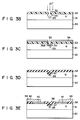
- Figs. 3A to 3E are sectional views of the structures of the device formed in manufacturing steps according to an embodiment in which the present invention is applied to a method of manufacturing an epitaxial growth J-FET.
- Zn+ is ion-implanted in layer 31 through opening portion 32 of film 33 and groove 34 of layer 31 under conditions that acceleration voltage V ac is 80 KeV and dosage Q d is 1 ⁇ 1015/cm2, thereby forming ion-implantation layer 35 in layer 31 at a region corresponding to groove 34.
- a 1,000- ⁇ thick lower TiW layer and a 5,000- ⁇ thick upper Au layer are formed in an Ar gas by sputtering, thereby forming conductor layer 36.
- the TiW layer is formed on film 16 and the Au layer is formed on the TiW layer.
- TiW and Au are sputtered on layer 35 through opening portion 32 formed in film 33 to form conductor layer 36A on layer 31.
- Materials other than TiW and Au may be used, as long as an ohmic contact between the layer formed of the materials and the gate region is not degraded, even when the layers are annealed in the following step.
- a single layer containing a refractory metal such as a WN layer or a WSi layer may be used.
- a bi-layered structure of a lower WN layer which contacts GaAs semiconductor layer 31 and an upper Au layer may be used. That is, any kind of layer may be used in place of the above layer as long as a layer contacting layer 31 is made of a refractory metal.
- layer 36 formed on the surface of film 33 is simultaneously removed. That is, layer 36 is removed by a so-called "lift off” method. As a result, only layer 36A remains formed on layer 31 to form gate electrode 37.
- PSG film 38 is formed by the CVD process on the entire major surface of the structure to have a thickness of 5,000 ⁇ . Then, the structure is annealed in an Ar gas at 800°C for 15 minutes to activate the impurity ion-implanted in layer 35, thereby forming P-type gate region 39. By way of this annealing process, gate electrode 37 is formed in ohmic contact with gate region 39.
- Source and drain leading electrodes 40 and 41 each comprising 2,000- ⁇ thick lower AuGe film containing 5% of Ge and a 1,000- ⁇ thick upper Au film are formed in the openings by, e.g., a lift-off method. Thereafter, the structure is annealed at 400°C for three minutes to form an ohmic contact between the source region and source leading electrode 40 and an ohmic contact between the drain region and drain leading electrode 41. Following this annealing process, source and drain electrodes 42 and 43 are formed on source and drain leading electrodes 40 and 41, respectively, by, e.g., a lift-off method. Source and drain electrodes 42 and 43 may be a superposed structure composed of a Ti layer - Pt layer - Au layer. In this way, the J-FET is completed.
- gate electrode 37 directly contacts gate region 39.
- a gate resistance can be sufficiently reduced, and a noise factor and a gain at a high frequency is not degraded.
- gate region 39 and gate electrode 37 are formed through opening portion 32 of film 33, by ion-implantation and sputtering, gate region 39 and gate electrode 37 are in self-alignment with each other. For this reason, even if region 39 is formed to occupy a small area, no positional deviation is generated between region 39 and electrode 37, resulting in high manufacturing yield.
- an FET in which a gate electrode can be positioned with respect to a small gate region with high accuracy and which is suitable for high frequency applications can be manufactured.
Landscapes
- Junction Field-Effect Transistors (AREA)
- Electrodes Of Semiconductors (AREA)
Applications Claiming Priority (2)
| Application Number | Priority Date | Filing Date | Title |
|---|---|---|---|
| JP62254146A JPH0195564A (ja) | 1987-10-08 | 1987-10-08 | 半導体装置の製造方法 |
| JP254146/87 | 1987-10-08 |
Publications (3)
| Publication Number | Publication Date |
|---|---|
| EP0311109A2 true EP0311109A2 (fr) | 1989-04-12 |
| EP0311109A3 EP0311109A3 (en) | 1989-07-12 |
| EP0311109B1 EP0311109B1 (fr) | 1994-01-05 |
Family
ID=17260862
Family Applications (1)
| Application Number | Title | Priority Date | Filing Date |
|---|---|---|---|
| EP88116670A Expired - Lifetime EP0311109B1 (fr) | 1987-10-08 | 1988-10-07 | Méthode de fabrication d'un transistor à effet de champ à porte à jonction |
Country Status (4)
| Country | Link |
|---|---|
| US (1) | US4895811A (fr) |
| EP (1) | EP0311109B1 (fr) |
| JP (1) | JPH0195564A (fr) |
| DE (1) | DE3886871T2 (fr) |
Families Citing this family (6)
| Publication number | Priority date | Publication date | Assignee | Title |
|---|---|---|---|---|
| US5273937A (en) * | 1988-01-08 | 1993-12-28 | Kabushiki Kaisha Toshiba | Metal semiconductor device and method for producing the same |
| US5011785A (en) * | 1990-10-30 | 1991-04-30 | The United States Of America As Represented By The Secretary Of The Navy | Insulator assisted self-aligned gate junction |
| DE4113969A1 (de) * | 1991-04-29 | 1992-11-05 | Telefunken Electronic Gmbh | Verfahren zur herstellung von ohmschen kontakten fuer verbindungshalbleiter |
| US5536677A (en) * | 1994-12-01 | 1996-07-16 | Motorola, Inc. | Method of forming conductive bumps on a semiconductor device using a double mask structure |
| US6609652B2 (en) * | 1997-05-27 | 2003-08-26 | Spheretek, Llc | Ball bumping substrates, particuarly wafers |
| US6051856A (en) * | 1997-09-30 | 2000-04-18 | Samsung Electronics Co., Ltd. | Voltage-controlled resistor utilizing bootstrap gate FET |
Family Cites Families (12)
| Publication number | Priority date | Publication date | Assignee | Title |
|---|---|---|---|---|
| DE2824026A1 (de) * | 1978-06-01 | 1979-12-20 | Licentia Gmbh | Verfahren zum herstellen eines sperrschicht-feldeffekttransistors |
| JPS57178376A (en) * | 1981-04-27 | 1982-11-02 | Sumitomo Electric Ind Ltd | Junction type field-effect transistor |
| JPS57178374A (en) * | 1981-04-27 | 1982-11-02 | Sumitomo Electric Ind Ltd | Junction type field-efect transistor and its manufacture |
| DE3150412A1 (de) * | 1981-12-19 | 1983-07-14 | Drägerwerk AG, 2400 Lübeck | Notatemschutzgeraet |
| JPS58143586A (ja) * | 1982-02-22 | 1983-08-26 | Toshiba Corp | 電界効果トランジスタの製造方法 |
| JPS58145158A (ja) * | 1982-02-23 | 1983-08-29 | Toshiba Corp | 電界効果トランジスタ及びその製造方法 |
| US4561169A (en) * | 1982-07-30 | 1985-12-31 | Hitachi, Ltd. | Method of manufacturing semiconductor device utilizing multilayer mask |
| JPS61163664A (ja) * | 1985-01-11 | 1986-07-24 | Mitsubishi Electric Corp | 半導体装置の製造方法 |
| JPS61177780A (ja) * | 1985-02-01 | 1986-08-09 | Mitsubishi Electric Corp | 半導体装置の製造方法 |
| FR2579827B1 (fr) * | 1985-04-01 | 1987-05-15 | Thomson Csf | Procede de realisation d'un transistor a effet de champ a metallisation de grille autoalignee |
| JPS6273676A (ja) * | 1985-09-26 | 1987-04-04 | Nec Corp | 接合型電界効果トランジスタの製造方法 |
| US4729967A (en) * | 1987-04-09 | 1988-03-08 | Gte Laboratories Incorporated | Method of fabricating a junction field effect transistor |
-
1987
- 1987-10-08 JP JP62254146A patent/JPH0195564A/ja active Granted
-
1988
- 1988-10-04 US US07/253,171 patent/US4895811A/en not_active Expired - Lifetime
- 1988-10-07 DE DE3886871T patent/DE3886871T2/de not_active Expired - Lifetime
- 1988-10-07 EP EP88116670A patent/EP0311109B1/fr not_active Expired - Lifetime
Also Published As
| Publication number | Publication date |
|---|---|
| JPH0543291B2 (fr) | 1993-07-01 |
| JPH0195564A (ja) | 1989-04-13 |
| US4895811A (en) | 1990-01-23 |
| DE3886871D1 (de) | 1994-02-17 |
| EP0311109B1 (fr) | 1994-01-05 |
| EP0311109A3 (en) | 1989-07-12 |
| DE3886871T2 (de) | 1994-06-09 |
Similar Documents
| Publication | Publication Date | Title |
|---|---|---|
| US4521952A (en) | Method of making integrated circuits using metal silicide contacts | |
| US4546540A (en) | Self-aligned manufacture of FET | |
| US5036017A (en) | Method of making asymmetrical field effect transistor | |
| US4446476A (en) | Integrated circuit having a sublayer electrical contact and fabrication thereof | |
| EP0378894A2 (fr) | Fabrication de circuits intégrés en GaAs | |
| US3909306A (en) | MIS type semiconductor device having high operating voltage and manufacturing method | |
| US4679311A (en) | Method of fabricating self-aligned field-effect transistor having t-shaped gate electrode, sub-micron gate length and variable drain to gate spacing | |
| US3943542A (en) | High reliability, low leakage, self-aligned silicon gate FET and method of fabricating same | |
| US5100813A (en) | Method of manufacturing bipolar transistor | |
| US4389768A (en) | Self-aligned process for fabricating gallium arsenide metal-semiconductor field effect transistors | |
| JPH07105392B2 (ja) | 突起部を有する半導体デバイス構造体 | |
| EP0073697B1 (fr) | Procédé pour la formation d'un transistor à effet de champ métal-semi-conducteur | |
| EP0178000A2 (fr) | Procédé de formation de rainures submicroniques, par exemple dans un matériau semi-conducteur et dispositifs obtenus selon ce procédé | |
| US6248666B1 (en) | Process of manufacturing a semiconductor device including a buried channel field effect transistor | |
| EP0305975A2 (fr) | MESFET à semi-conducteur composé | |
| CA1179786A (fr) | Transistor a structure laterale ayant une base auto-alignee et un contact de base et methode de fabrication | |
| US5693544A (en) | N-type higfet and method | |
| US4523368A (en) | Semiconductor devices and manufacturing methods | |
| EP0311109A2 (fr) | Méthode de fabrication d'un transistor à effet de champ à porte à jonction | |
| US4804635A (en) | Method of manufacture of galluim arsenide field effect transistors | |
| US4675713A (en) | MOS transistor | |
| US5231040A (en) | Method of making a field effect transistor | |
| US4054989A (en) | High reliability, low leakage, self-aligned silicon gate FET and method of fabricating same | |
| US4956689A (en) | High speed gallium arsenide transistor and method | |
| US5597743A (en) | Method of manufacturing a field effect transistor with improved isolation between electrode |
Legal Events
| Date | Code | Title | Description |
|---|---|---|---|
| PUAI | Public reference made under article 153(3) epc to a published international application that has entered the european phase |
Free format text: ORIGINAL CODE: 0009012 |
|
| 17P | Request for examination filed |
Effective date: 19881007 |
|
| AK | Designated contracting states |
Kind code of ref document: A2 Designated state(s): DE FR GB |
|
| PUAL | Search report despatched |
Free format text: ORIGINAL CODE: 0009013 |
|
| AK | Designated contracting states |
Kind code of ref document: A3 Designated state(s): DE FR GB |
|
| 17Q | First examination report despatched |
Effective date: 19910813 |
|
| GRAA | (expected) grant |
Free format text: ORIGINAL CODE: 0009210 |
|
| AK | Designated contracting states |
Kind code of ref document: B1 Designated state(s): DE FR GB |
|
| REF | Corresponds to: |
Ref document number: 3886871 Country of ref document: DE Date of ref document: 19940217 |
|
| ET | Fr: translation filed | ||
| PLBE | No opposition filed within time limit |
Free format text: ORIGINAL CODE: 0009261 |
|
| STAA | Information on the status of an ep patent application or granted ep patent |
Free format text: STATUS: NO OPPOSITION FILED WITHIN TIME LIMIT |
|
| 26N | No opposition filed | ||
| PGFP | Annual fee paid to national office [announced via postgrant information from national office to epo] |
Ref country code: GB Payment date: 19970929 Year of fee payment: 10 |
|
| PGFP | Annual fee paid to national office [announced via postgrant information from national office to epo] |
Ref country code: FR Payment date: 19971009 Year of fee payment: 10 |
|
| PG25 | Lapsed in a contracting state [announced via postgrant information from national office to epo] |
Ref country code: GB Free format text: LAPSE BECAUSE OF NON-PAYMENT OF DUE FEES Effective date: 19981007 |
|
| GBPC | Gb: european patent ceased through non-payment of renewal fee |
Effective date: 19981007 |
|
| PG25 | Lapsed in a contracting state [announced via postgrant information from national office to epo] |
Ref country code: FR Free format text: LAPSE BECAUSE OF NON-PAYMENT OF DUE FEES Effective date: 19990630 |
|
| REG | Reference to a national code |
Ref country code: FR Ref legal event code: ST |
|
| PGFP | Annual fee paid to national office [announced via postgrant information from national office to epo] |
Ref country code: DE Payment date: 20071004 Year of fee payment: 20 |