EP0314226A2 - Integrierte Struktur mit aktiven und passiven Komponenten in isolierten Wannen, die mit höheren als die Durchbruchsspannung zwischen jeder Komponente und der entsprechenden Wanne betrieben werden - Google Patents
Integrierte Struktur mit aktiven und passiven Komponenten in isolierten Wannen, die mit höheren als die Durchbruchsspannung zwischen jeder Komponente und der entsprechenden Wanne betrieben werden Download PDFInfo
- Publication number
- EP0314226A2 EP0314226A2 EP88202271A EP88202271A EP0314226A2 EP 0314226 A2 EP0314226 A2 EP 0314226A2 EP 88202271 A EP88202271 A EP 88202271A EP 88202271 A EP88202271 A EP 88202271A EP 0314226 A2 EP0314226 A2 EP 0314226A2
- Authority
- EP
- European Patent Office
- Prior art keywords
- breakdown voltage
- insulating
- integrated structure
- voltage
- Prior art date
- Legal status (The legal status is an assumption and is not a legal conclusion. Google has not performed a legal analysis and makes no representation as to the accuracy of the status listed.)
- Withdrawn
Links
Images


Classifications
-
- H—ELECTRICITY
- H10—SEMICONDUCTOR DEVICES; ELECTRIC SOLID-STATE DEVICES NOT OTHERWISE PROVIDED FOR
- H10D—INORGANIC ELECTRIC SEMICONDUCTOR DEVICES
- H10D84/00—Integrated devices formed in or on semiconductor substrates that comprise only semiconducting layers, e.g. on Si wafers or on GaAs-on-Si wafers
- H10D84/60—Integrated devices formed in or on semiconductor substrates that comprise only semiconducting layers, e.g. on Si wafers or on GaAs-on-Si wafers characterised by the integration of at least one component covered by groups H10D10/00 or H10D18/00, e.g. integration of BJTs
- H10D84/611—Combinations of BJTs and one or more of diodes, resistors or capacitors
- H10D84/613—Combinations of vertical BJTs and one or more of diodes, resistors or capacitors
- H10D84/615—Combinations of vertical BJTs and one or more of resistors or capacitors
-
- H—ELECTRICITY
- H10—SEMICONDUCTOR DEVICES; ELECTRIC SOLID-STATE DEVICES NOT OTHERWISE PROVIDED FOR
- H10W—GENERIC PACKAGES, INTERCONNECTIONS, CONNECTORS OR OTHER CONSTRUCTIONAL DETAILS OF DEVICES COVERED BY CLASS H10
- H10W10/00—Isolation regions in semiconductor bodies between components of integrated devices
- H10W10/01—Manufacture or treatment
- H10W10/031—Manufacture or treatment of isolation regions comprising PN junctions
-
- H—ELECTRICITY
- H10—SEMICONDUCTOR DEVICES; ELECTRIC SOLID-STATE DEVICES NOT OTHERWISE PROVIDED FOR
- H10W—GENERIC PACKAGES, INTERCONNECTIONS, CONNECTORS OR OTHER CONSTRUCTIONAL DETAILS OF DEVICES COVERED BY CLASS H10
- H10W10/00—Isolation regions in semiconductor bodies between components of integrated devices
- H10W10/30—Isolation regions comprising PN junctions
Definitions
- the present invention relates to an integrated structure with active and passive components enclosed in insulating pockets and operating at a voltage higher, compared to ground, than the breakdown voltage between each component and the pocket containing it.
- the object of the present invention is to accomplish an integrated structure which could operate with a higher than breakdown voltage between each component and the insulating pocket containing it.
- said object is achieved by providing an integrated structure consisting of circuital components made by diffusion of dopes in a semiconductor substrate, each of said circuital components being located inside an insulating pocket, characterized in that each insulating pocket is connected to a voltage falling between the minimum and maximum voltages applied to the components contained in the corresponding pocket, the breakdown voltage between the insulating pocket and the surrounding semiconductor substrate being much higher than the breakdown voltage between the insulating pocket and the component contained therein.
- the breakdown voltage between the substrate and the insulating pocket is much higher than the breakdown voltage between the pocket and the components contained therein, said components can be supplied with a voltage higher than the breakdown voltage between the pocket and the substrate without any inconvenience. Indeed, the maximum voltage compared to ground applied to a component of the pocket no longer depends on the breakdown voltage between that component and the insulating pocket.
- insulating pockets In determining the insulating pockets it is necessary that they be appropriately spaced so that two adjacent insulating pockets separated by a substrate zone constitute a transistor with high breakdown voltage BV ceo wherein the substrate forms the base and the insulating pockets form the emitter and the collector.
- FIG. 1 an integrated structure created in accordance with the invention is shown therein.
- the structure comprises a semiconductor substrate 1 with n+ doping having an epitaxial layer 2 formed in accordance with known techniques with two superimposed layers 3 and 4.
- Said epitaxial layer 2 contains two separate insulating pockets 5 with p doping in the deeper part 6 and p+ doping in the surface parts 7.
- Each insulating pocket 5 contains in turn a buried n+ layer 8, an intermediate n ⁇ layer 9, and a p surface area 10.
- a first surface zone with n+ doping 11 is provided.
- a second n+ doped zone 12 is provided within the intermediate area 9.
- Said doped zones 10, 11, 12 determine inside the pockets 5 respective npn transistors 20 and 21.
- the surface of the epitaxial layer 3 is covered with a layer of oxide 13.
- Surface contacts 14, 15, 16 and 17 are placed respectively in positions corresponding with those of one of the surface parts 7 of the insulating pockets 5 and of a collector area on the zone 12, base area on the zones 10, and emitter area on the zones 11.
- the intermediate layer 9 and the insulating pocket 5 are equivalent to a diode D1 while the insulating pocket 5 and the substrate 1,2 are equivalent to a second diode D2.
- the breakdown voltage of the diodes D2 be higher than the breakdown voltage of the diode DI.
- the epitaxial layer 2 must be connected to a positive voltage in relation to the insulating pockets 5 to avoid establishing direct contact of the diode D2 or D3 between pocket 5 and layer 2.
- the contact of the collector 15 is supplied with a voltage V1 and the emitter contact 17 is supplied with a voltage V2 in which V1 is greater than V2.
- the contact 14 of the insulating pocket 5 is connected to a voltage V3 falling between V1 and V2, the latter being supplied by two batteries VA and VB, which are variable if V1-V2 is variable.
- the transistors 20 and 21 shown in FIG. 1 may be accomplished in the form shown in FIGS. 2 and 3 in which another contact 18 is provided in the base zone 10, said contact 18 being connected to the emitter contact 17 by a metallization 19.
- the invention can also be applied for example to the pilot circuit of the high part of a semibridge as shown in FIG. 4.
- the semibridge includes two input terminals 40 and 45 and an output terminal 41, transistors 42 and 43 which determine the semibridge, an input transistor 44 and transistors T1 and T2 to pilot the high part of the semibridge with a voltage shift.
- the transistors T1 and T2 are combined with resistances R1, R2, R3.
- the transistors T1 and T2 are illustrated in FIG. 5 together with the parasite components.
- the transistors T1 and T2 consist of npn doped surface zones 51, 52 and 53 in which the surface collector zone 53 is immersed in the intermediate n ⁇ layer 9 as far as the buried n+ layer 8.
- the intermediate layer 9 is always contained in a pocket 5, which is in turn immersed in the epitaxial layer 2, which is arranged on the substrate 1.
- the pockets 5 and the intermediate layers 9 of the two transistors T1 and T2 constitute respectively diodes D1 and D2 just as the pockets 5 and the epitaxial layer 2 constitute the diodes D4 and D3.
- the breakdown voltage of the diodes D3 and D4 must of course be higher than the breakdown voltage of the diodes D1 and D2.
- the transistor T5 schematizes the pnp transistor made up of the pockets 5 of the two transistors T1 and T2 separated from the layer 2 in which the layer 2 constitutes the base and the pockets 5 constitute the emitter and the collector.
- the transistors T3 and T6 schematize the npn transistors made up of the doped zone 53 which acts as an emitter, the pocket 5 which acts as a base, and the layer 2 which acts as a collector.
- the transistors T4 and T7 schematize the pnp transistors made up of the doped zone 52 which acts as an emitter, the zone 53 wich acts as a base, and the pocket 5 which acts as a collector.
- the pockets 5 must be appropriately spaced so that the parasite transistor T5 will not reach breakdown voltage at the maximum potential difference applied between the two pockets 5.
- the transistors T4 and T1 form an SCR which tends to fire if D4 has a current loss.
- T7 and T2 also form an SCR which tends to fire if D3 has a current loss.
- One way of eliminating firing of the parasite SCRs is to short circuit the base and emitter of T4 and T7 as indicated in dash & dot lines in FIGS. 5 and 6, which is equivalent to connecting the pocket 5 to the respective intermediate layer 9 contained therein.
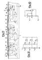
- the transistor T1 can have on the collector a voltage higher, compared with ground, than the breakdown voltage between the pocket 5 and the intermediate layer; said applicable voltage is limited only by the breadkown voltage between the layer 2 and the insulating pocket 5.
- a similar result is obtained if the emitter 51 of the transistor is connected to the respective insulating pocket 5 using an appropriate metallic contact 55 as shown in FIGS. 7 and 8.
- the parasite components T13-T17 are polarized in reverse in relation to the parasite components T3-T7 of FIG. 5.
- the pockets 5 are contained in an n ⁇ epitaxial layer 25 and contain an n intermediate layer 26 and a buried layer 8.
- the layer 25 is in turn formed of the layers 27 and 28.
- a resistance R consisting of surface zones 60 and 61 with p and n+ doping are contained in an intermediate n ⁇ layer 62 has been made.
- a buried n+ layer 8 is placed between said intermediate layer 62 and the insulating pocket 5 contained in an epitaxial layer 63 placed on the substrate 1.
- the pocket 5 and the epitaxial layer 63 constitute the diode D10 and in addition there are present the parasite transistors T21 and T22 in which the transistor T21 is npn with the emitter consisting of the zone 61, the base of the pocket 5 and the collector of the epitaxial layer 63, and the transistor T22 is pnp in which the base consists of the intermediate layer 62 and the collector and emitter of the pocket 5 and the zone 60 respectively.
- the maximum voltage V1 applicable to the resistance is limited by the breakdown voltage of the diode D10.
- each pocket 5 has a contact 66 connected to one end 64 of the resistance contained in that pocket.
- the contact 66 can also be connected to the end 65 or to any intermediate point of the resistance.
- the supply voltage V is independent of the breakdown voltage of the diode made up of the insulating pocket 5 and the intermediate layer 62.
Landscapes
- Bipolar Integrated Circuits (AREA)
- Element Separation (AREA)
- Bipolar Transistors (AREA)
- Semiconductor Integrated Circuits (AREA)
Applications Claiming Priority (2)
| Application Number | Priority Date | Filing Date | Title |
|---|---|---|---|
| IT8722474A IT1232930B (it) | 1987-10-30 | 1987-10-30 | Struttura integrata a componenti attivi e passivi inclusi in sacche di isolamento operante a tensione maggiore della tensione di rottura tra ciascun componente e la sacca che lo contiene |
| IT2247487 | 1987-10-30 |
Publications (2)
| Publication Number | Publication Date |
|---|---|
| EP0314226A2 true EP0314226A2 (de) | 1989-05-03 |
| EP0314226A3 EP0314226A3 (de) | 1989-11-15 |
Family
ID=11196764
Family Applications (1)
| Application Number | Title | Priority Date | Filing Date |
|---|---|---|---|
| EP88202271A Withdrawn EP0314226A3 (de) | 1987-10-30 | 1988-10-11 | Integrierte Struktur mit aktiven und passiven Komponenten in isolierten Wannen, die mit höheren als die Durchbruchsspannung zwischen jeder Komponente und der entsprechenden Wanne betrieben werden |
Country Status (4)
| Country | Link |
|---|---|
| US (1) | US4947231A (de) |
| EP (1) | EP0314226A3 (de) |
| JP (1) | JP2686500B2 (de) |
| IT (1) | IT1232930B (de) |
Cited By (1)
| Publication number | Priority date | Publication date | Assignee | Title |
|---|---|---|---|---|
| WO2002011199A3 (de) * | 2000-08-01 | 2002-06-27 | Infineon Technologies Ag | Nachführschaltung |
Families Citing this family (10)
| Publication number | Priority date | Publication date | Assignee | Title |
|---|---|---|---|---|
| USRE35642E (en) * | 1987-12-22 | 1997-10-28 | Sgs-Thomson Microelectronics, S.R.L. | Integrated high-voltage bipolar power transistor and low voltage MOS power transistor structure in the emitter switching configuration and relative manufacturing process |
| IT1217323B (it) * | 1987-12-22 | 1990-03-22 | Sgs Microelettronica Spa | Struttura integrata di transistor bipolare di potenza di alta tensione e di transistor mos di potenza di bassa tensione nella configurazione"emitter switching"e relativo processo di fabbricazione |
| US5156989A (en) * | 1988-11-08 | 1992-10-20 | Siliconix, Incorporated | Complementary, isolated DMOS IC technology |
| IT1230895B (it) * | 1989-06-22 | 1991-11-08 | Sgs Thomson Microelectronics | Transistore di potenza integrabile con ottimizzazione dei fenomeni di rottura secondaria diretta. |
| US5410175A (en) * | 1989-08-31 | 1995-04-25 | Hamamatsu Photonics K.K. | Monolithic IC having pin photodiode and an electrically active element accommodated on the same semi-conductor substrate |
| IT1236667B (it) * | 1989-11-07 | 1993-03-25 | Sgs Thomson Microelectronics | Dispositivo di protezione contro la rottura di una regione diffusa di tipo n+ inserita in una struttura integrata di potenza a semiconduttore di tipo verticale |
| US5311054A (en) * | 1991-03-25 | 1994-05-10 | Harris Corporation | Graded collector for inductive loads |
| EP0579045B1 (de) * | 1992-07-16 | 1995-02-22 | Landis & Gyr Technology Innovation AG | Anordnung mit einer integrierten farbselektiven Photodiode und einem der Photodiode nachgeschalteten Verstärker |
| EP0646964B1 (de) * | 1993-09-30 | 1999-12-15 | Consorzio per la Ricerca sulla Microelettronica nel Mezzogiorno | Integrierte aktive Klammerungsstruktur für den Schutz von Leistungsanordnungen gegen Überspannungen, und Verfahren zu ihrer Herstellung |
| JP2020009790A (ja) * | 2016-11-09 | 2020-01-16 | シャープ株式会社 | アバランシェフォトダイオード |
Family Cites Families (13)
| Publication number | Priority date | Publication date | Assignee | Title |
|---|---|---|---|---|
| US3547716A (en) * | 1968-09-05 | 1970-12-15 | Ibm | Isolation in epitaxially grown monolithic devices |
| US4233618A (en) * | 1978-07-31 | 1980-11-11 | Sprague Electric Company | Integrated circuit with power transistor |
| FR2492165A1 (fr) * | 1980-05-14 | 1982-04-16 | Thomson Csf | Dispositif de protection contre les courants de fuite dans des circuits integres |
| FR2543364B1 (fr) * | 1983-03-25 | 1986-09-05 | Trt Telecom Radio Electr | Procede de realisation de transistors par integration monolithique en technologie bipolaire et circuits integres ainsi obtenus |
| JPS59191348A (ja) * | 1983-04-14 | 1984-10-30 | Sanyo Electric Co Ltd | 半導体集積回路 |
| JPS6079736A (ja) * | 1983-10-06 | 1985-05-07 | Sanyo Electric Co Ltd | 半導体集積回路 |
| US4646124A (en) * | 1984-07-30 | 1987-02-24 | Sprague Electric Company | Level shifting BIMOS integrated circuit |
| IT1214806B (it) * | 1984-09-21 | 1990-01-18 | Ates Componenti Elettron | Dispositivo integrato monolitico di potenza e semiconduttore |
| FR2571178B1 (fr) * | 1984-09-28 | 1986-11-21 | Thomson Csf | Structure de circuit integre comportant des transistors cmos a tenue en tension elevee, et son procede de fabrication |
| JPS61234075A (ja) * | 1985-04-10 | 1986-10-18 | Sanyo Electric Co Ltd | コイル負荷駆動用半導体集積回路 |
| US4684970A (en) * | 1985-07-29 | 1987-08-04 | Rca Corporation | High current lateral transistor structure |
| GB2186117B (en) * | 1986-01-30 | 1989-11-01 | Sgs Microelettronica Spa | Monolithically integrated semiconductor device containing bipolar junction,cmosand dmos transistors and low leakage diodes and a method for its fabrication |
| IT1204244B (it) * | 1986-03-21 | 1989-03-01 | Sgs Microelettronica Spa | Struttura npn equivalente con tensione di rottura maggiorata rispetto alla tensione di rottura intrinseca dell'npn |
-
1987
- 1987-10-30 IT IT8722474A patent/IT1232930B/it active
-
1988
- 1988-10-11 EP EP88202271A patent/EP0314226A3/de not_active Withdrawn
- 1988-10-18 US US07/259,254 patent/US4947231A/en not_active Expired - Lifetime
- 1988-10-27 JP JP63269642A patent/JP2686500B2/ja not_active Expired - Fee Related
Cited By (2)
| Publication number | Priority date | Publication date | Assignee | Title |
|---|---|---|---|---|
| WO2002011199A3 (de) * | 2000-08-01 | 2002-06-27 | Infineon Technologies Ag | Nachführschaltung |
| US6800926B2 (en) | 2000-08-01 | 2004-10-05 | Infineon Technologies Ag | Tracking circuit |
Also Published As
| Publication number | Publication date |
|---|---|
| JPH01146352A (ja) | 1989-06-08 |
| EP0314226A3 (de) | 1989-11-15 |
| JP2686500B2 (ja) | 1997-12-08 |
| IT1232930B (it) | 1992-03-10 |
| US4947231A (en) | 1990-08-07 |
| IT8722474A0 (it) | 1987-10-30 |
Similar Documents
| Publication | Publication Date | Title |
|---|---|---|
| US5652689A (en) | ESD protection circuit located under protected bonding pad | |
| EP0314226A2 (de) | Integrierte Struktur mit aktiven und passiven Komponenten in isolierten Wannen, die mit höheren als die Durchbruchsspannung zwischen jeder Komponente und der entsprechenden Wanne betrieben werden | |
| EP0388180A1 (de) | Halbleitervorrichtung mit Schutz-Schaltkreis | |
| US4969030A (en) | Integrated structure for a signal transfer network, in particular for a pilot circuit for MOS power transistors | |
| US3666995A (en) | Integrated semiconductor device | |
| EP0136868A2 (de) | Halbleiteranordnung mit Schutzelementen | |
| US4309626A (en) | Diffused resistor | |
| US4631570A (en) | Integrated circuit having buried oxide isolation and low resistivity substrate for power supply interconnection | |
| US5541439A (en) | Layout for a high voltage darlington pair | |
| EP0330299A2 (de) | Teilkundenspezifische integrierte Schaltung | |
| US4642668A (en) | Semiconductor device having improved thermal characteristics | |
| US3755722A (en) | Resistor isolation for double mesa transistors | |
| US4812891A (en) | Bipolar lateral pass-transistor for CMOS circuits | |
| KR20040002654A (ko) | 반도체 집적 회로 장치 | |
| EP0577906B1 (de) | Struktur zur Vermeidung des Durchschaltens einer parasitären Diode, die sich in einer epitaktischen Wanne von integrierten Schaltungen befindet | |
| US4158146A (en) | Device for coupling transistors operated in I2 L to a transistor operated at a higher bias-current | |
| JPS6348192B2 (de) | ||
| US4547743A (en) | Variable resistance gain control integrated circuit | |
| US4814852A (en) | Controlled voltage drop diode | |
| US3544860A (en) | Integrated power output circuit | |
| US4160986A (en) | Bipolar transistors having fixed gain characteristics | |
| JP3390040B2 (ja) | 集積回路 | |
| JPS63148671A (ja) | 半導体集積回路装置の静電破壊防止装置 | |
| US4851893A (en) | Programmable active/passive cell structure | |
| JPS6098659A (ja) | 直列接続トランジスタを有する半導体集積回路 |
Legal Events
| Date | Code | Title | Description |
|---|---|---|---|
| PUAI | Public reference made under article 153(3) epc to a published international application that has entered the european phase |
Free format text: ORIGINAL CODE: 0009012 |
|
| AK | Designated contracting states |
Kind code of ref document: A2 Designated state(s): DE FR GB NL SE |
|
| PUAL | Search report despatched |
Free format text: ORIGINAL CODE: 0009013 |
|
| AK | Designated contracting states |
Kind code of ref document: A3 Designated state(s): DE FR GB NL SE |
|
| 17P | Request for examination filed |
Effective date: 19900319 |
|
| 17Q | First examination report despatched |
Effective date: 19921203 |
|
| STAA | Information on the status of an ep patent application or granted ep patent |
Free format text: STATUS: THE APPLICATION IS DEEMED TO BE WITHDRAWN |
|
| 18D | Application deemed to be withdrawn |
Effective date: 19970416 |