EP0315213A2 - Vertikale MOSFET-Vorrichtung mit Schutz - Google Patents
Vertikale MOSFET-Vorrichtung mit Schutz Download PDFInfo
- Publication number
- EP0315213A2 EP0315213A2 EP88118526A EP88118526A EP0315213A2 EP 0315213 A2 EP0315213 A2 EP 0315213A2 EP 88118526 A EP88118526 A EP 88118526A EP 88118526 A EP88118526 A EP 88118526A EP 0315213 A2 EP0315213 A2 EP 0315213A2
- Authority
- EP
- European Patent Office
- Prior art keywords
- region
- conductivity type
- mosfet device
- protector
- vertical mosfet
- Prior art date
- Legal status (The legal status is an assumption and is not a legal conclusion. Google has not performed a legal analysis and makes no representation as to the accuracy of the status listed.)
- Granted
Links
- 230000001012 protector Effects 0.000 title claims abstract description 23
- 239000004065 semiconductor Substances 0.000 claims abstract description 11
- 229910021420 polycrystalline silicon Inorganic materials 0.000 claims description 14
- 230000015556 catabolic process Effects 0.000 description 8
- 239000000758 substrate Substances 0.000 description 4
- 230000000694 effects Effects 0.000 description 3
- 238000010276 construction Methods 0.000 description 2
- 230000006378 damage Effects 0.000 description 2
- 230000036961 partial effect Effects 0.000 description 2
- 230000002829 reductive effect Effects 0.000 description 2
- XUIMIQQOPSSXEZ-UHFFFAOYSA-N Silicon Chemical compound [Si] XUIMIQQOPSSXEZ-UHFFFAOYSA-N 0.000 description 1
- XAGFODPZIPBFFR-UHFFFAOYSA-N aluminium Chemical compound [Al] XAGFODPZIPBFFR-UHFFFAOYSA-N 0.000 description 1
- 229910052782 aluminium Inorganic materials 0.000 description 1
- 239000004411 aluminium Substances 0.000 description 1
- 230000007547 defect Effects 0.000 description 1
- 230000003292 diminished effect Effects 0.000 description 1
- 230000005611 electricity Effects 0.000 description 1
- 230000000670 limiting effect Effects 0.000 description 1
- 230000000873 masking effect Effects 0.000 description 1
- 239000007769 metal material Substances 0.000 description 1
- 230000035945 sensitivity Effects 0.000 description 1
- 229910052710 silicon Inorganic materials 0.000 description 1
- 239000010703 silicon Substances 0.000 description 1
- 230000003068 static effect Effects 0.000 description 1
Images

Classifications
-
- H—ELECTRICITY
- H10—SEMICONDUCTOR DEVICES; ELECTRIC SOLID-STATE DEVICES NOT OTHERWISE PROVIDED FOR
- H10D—INORGANIC ELECTRIC SEMICONDUCTOR DEVICES
- H10D84/00—Integrated devices formed in or on semiconductor substrates that comprise only semiconducting layers, e.g. on Si wafers or on GaAs-on-Si wafers
- H10D84/101—Integrated devices comprising main components and built-in components, e.g. IGBT having built-in freewheel diode
- H10D84/141—VDMOS having built-in components
- H10D84/143—VDMOS having built-in components the built-in components being PN junction diodes
-
- H—ELECTRICITY
- H10—SEMICONDUCTOR DEVICES; ELECTRIC SOLID-STATE DEVICES NOT OTHERWISE PROVIDED FOR
- H10D—INORGANIC ELECTRIC SEMICONDUCTOR DEVICES
- H10D89/00—Aspects of integrated devices not covered by groups H10D84/00 - H10D88/00
- H10D89/60—Integrated devices comprising arrangements for electrical or thermal protection, e.g. protection circuits against electrostatic discharge [ESD]
- H10D89/601—Integrated devices comprising arrangements for electrical or thermal protection, e.g. protection circuits against electrostatic discharge [ESD] for devices having insulated gate electrodes, e.g. for IGFETs or IGBTs
- H10D89/611—Integrated devices comprising arrangements for electrical or thermal protection, e.g. protection circuits against electrostatic discharge [ESD] for devices having insulated gate electrodes, e.g. for IGFETs or IGBTs using diodes as protective elements
Definitions
- the present invention relates to a vertical MOSFET device having a protector for preventing its breakdown due to heat increase or the like.
- Fig. 1 there is shown a conventional vertical MOSFET device, as disclosed in Japanese Patent Laid-Open Specification No. 60-258967.
- an n-type high resistance epitaxial layer 12 is grown on an n+-type low resistance substrate 11, and p-type base region 13 having a conductivity type different from that of the epitaxial layer 12 is formed in an upper surface area thereof.
- An n+-type source region 14 having the same conductivity type as that of the epitaxial layer 12 is formed in a central upper surface area of the p-type base region 13, and a p+-type base contact region 15 is formed in the left side surface area of the p-type base region 13.
- An insulating gate film 16 is formed on the surfaces of the right side of the epitaxial layer 12, the p-type base region 13 and the overlapping part of the source region 14.
- a gate electrode 17 is then formed over the entire surface of the insulating gate film 16.
- a source electrode 18 is formed extending over the partial surfaces of the N+-type source region 14 and the p+-type base contact region 15.
- the gate electrode 17, the source electrode 18 and the semiconductor substrate 11 are connected to a gate terminal C, a source terminal S and a drain terminal D, respectively.
- FIG. 2 An area of safety operation (ASO) of the conventional vertical MOSFET device shown in Fig. 1.
- the ASO is defined by three characteristic lines 21, 22 and 23 which represent the limitations by the maximum current, the maximum consumption power and the maximum voltage, respectively.
- a vertical MOSFET device comprising a semiconductor layer having a first conductivity type, a base region having a second conductivity type, formed in a surface portion of the semiconductor layer, a source region having the first conductivity type, formed in the base region, a gate electrode formed at least on the base region via an insulating gate film interposed therebetween to form a channel between the semiconductor layer and the source region, and a protector having one of PN junction and Schottky junction, which is formed between the source region and the gate electrode and is thermally contacted with at least one of the other members.
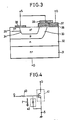
- FIGs. 3 and 4 the first embodiment of a vertical MOSFET device having a protector according to the present invention.
- an n-type high resistance epitaxial layer 32 is grown on an n+-type low resistance substrate 31 such as a silicon semiconductor substrate, and a p-type base region 33 having a conductivity type different from that of the epitaxial layer 32 is formed in an upper surface area thereof.
- An n+-type source region 34 having the same conductivity type as that of the epitaxial layer 32 is formed in a central upper surface area of the p-type base region 33, and a p+-type base contact region 35 is formed in the left side surface area of the p-type base region 33.
- An insulating gate film 36 is formed over the surfaces of the right side of the n-type epitaxial layer 32 and the p-type base region 33, operlapping into part of the source region 34, and an n+-type polycrystalline film 37 having the same conductivity type as that of the n+-type source region 34 is formed as a gate electrode on the entire surface of the insulating gate film 36.
- a p+-type polycrystalline silicon film 39 having a conductivity type different from that of the polycrystalline film 37 is formed thereon to constitute a PN junction therebetween.
- a source electrode 38 is formed extending over the partial surfaces of the n+-type source region 34 and the p+-type base contact region 35, and is electrically connected to the polycrystalline silicon film 39.
- FIG. 4 there is shown an equivalent circuit of the vertical MOSFET device described above, including a vertical MOSFET 41 comprised of the components 31 to 38, a protector diode 42 which is integrally attached to the MOSFET 41 and is composed of the polycrystalline silicon films 37 and 39 having the PN junction therebetween, and an input resistor (not shown in Fig. 3) for restricting a gate voltage.
- the protector diode 42 comprised of the polycrystalline silicon films 37 and 39 is thermally contacted with the vertical MOSFET 41, when the temperature of the MOSFET 41 is raised due to the overload or the like, the junction temperature of the protector diode 42 rises, and the leakage current I flowing through the protector diode 42 increases exponentially. Hence, the gate voltage of the MOSFET 41 is reduced, and the current flowing the the MOSFET 41 and the consumption power therein are automatically reduced, resulting in that the temperature rise of the MOSFET 41 is limited and the MOSFET 41 is protected from the breakdown due to the temperature rise.
- the protector diode 42 is provided integrally on the gate electrode portion, and the area and size of the protector diode 42 can be diminished as compared with an external protecting circuit attached to the conventional MOSFET device. Further, in this embodiment, the sensitivity to the temperature rise can be also largely improved as compared with the conventional MOSFET device.
- a metallic material such as aluminium can be used instead of the polycrystalline silicon film 39 of the first embodiment shown in Fig. 1.
- the metallic electrode and the polycrystalline silicon film 39 constitute a Schottky junction therebetween with the same effects and results as those of the first embodiment.
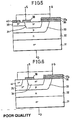
- Fig. 5 there is shown the second embodiment of the vertical MOSFET device according to the present invention, having the same construction as that of the prior art described above, except the base contact region. That is, an n+-type polycrystalline silicon film 40 having a conductivity type different from that of the p+-type base contact region 35 is formed thereon separate from the source electrode 38. The polycrystalline silicon film 40 is electrically connected to the gate electrode 37a.
- the base contact region 35 and the polycrystalline silicon film 40 constitute the protector diode 42 which functions in the same manner as that of the first embodiment with the same effects and advantages as those obtained in the first embodiment.
- Fig. 6 there is shown the third embodiment of the vertical MOSFET device according to the present invention, having the same construction as that of the second embodiment described above, except that the p+-type base contact region 35 is formed more deeply through the p-type base region 33 to contact the n-type epitaxial layer 32, and an n+-type region 41 is formed in the surface area of the base contact region 35 instead of the n+-type polycrystalline silicon film 40 of the second embodiment.
- the n+-type region 41 and the base contact region 35 constitute a PN junction protector diode instead of the protector diode composed of the polycrystalline silicon film 40 and the base contact region 35 in the second embodiment.
- the protector forming region 41 can be prepared along with the source region 34 in one step, and thus the vertical MOSFET device can be readily produced without providing particular masking and processing steps.
- the protector diode 42 acts as a Zener diode for limiting the gate voltage, and the electrostatic charge flows down into the source through the Zener diode, thereby reducing the breakdown of the insulating gate film due to the static electricity.
Landscapes
- Metal-Oxide And Bipolar Metal-Oxide Semiconductor Integrated Circuits (AREA)
- Electrodes Of Semiconductors (AREA)
Applications Claiming Priority (2)
| Application Number | Priority Date | Filing Date | Title |
|---|---|---|---|
| JP62279099A JPH081956B2 (ja) | 1987-11-06 | 1987-11-06 | 保護機能を備えた縦型mosfet |
| JP279099/87 | 1987-11-06 |
Publications (3)
| Publication Number | Publication Date |
|---|---|
| EP0315213A2 true EP0315213A2 (de) | 1989-05-10 |
| EP0315213A3 EP0315213A3 (en) | 1990-11-07 |
| EP0315213B1 EP0315213B1 (de) | 1995-02-08 |
Family
ID=17606401
Family Applications (1)
| Application Number | Title | Priority Date | Filing Date |
|---|---|---|---|
| EP88118526A Expired - Lifetime EP0315213B1 (de) | 1987-11-06 | 1988-11-07 | Vertikale MOSFET-Vorrichtung mit Schutz |
Country Status (4)
| Country | Link |
|---|---|
| US (1) | US4963970A (de) |
| EP (1) | EP0315213B1 (de) |
| JP (1) | JPH081956B2 (de) |
| DE (1) | DE3852986T2 (de) |
Cited By (3)
| Publication number | Priority date | Publication date | Assignee | Title |
|---|---|---|---|---|
| EP0595355A1 (de) * | 1992-10-30 | 1994-05-04 | Kabushiki Kaisha Toshiba | Halbleiteranordnung mit einem Schutzelement und Verfahren zu ihrer Herstellung |
| EP0646964A1 (de) * | 1993-09-30 | 1995-04-05 | Consorzio per la Ricerca sulla Microelettronica nel Mezzogiorno - CoRiMMe | Integrierte aktive Klammerungsstruktur für den Schutz von Leistungsanordnungen gegen Überspannungen, und Verfahren zu ihrer Herstellung |
| WO2002041404A3 (en) * | 2000-11-17 | 2002-10-10 | Koninkl Philips Electronics Nv | Trench-gate field-effect transistors and their manufacture |
Families Citing this family (19)
| Publication number | Priority date | Publication date | Assignee | Title |
|---|---|---|---|---|
| DE4134855C2 (de) * | 1990-10-31 | 2001-03-15 | Fuji Electric Co Ltd | MOS-Halbleiterelement |
| JP3218642B2 (ja) * | 1991-09-27 | 2001-10-15 | 富士電機株式会社 | 大電流集積回路の配線構造 |
| EP0601823B1 (de) * | 1992-12-09 | 2000-10-11 | Compaq Computer Corporation | Herstellung eines Feldeffekttransistors mit integrierter Schottky-Klammerungsdiode |
| JP3405364B2 (ja) * | 1993-03-08 | 2003-05-12 | セイコーインスツルメンツ株式会社 | 半導体装置 |
| DE4308624A1 (de) * | 1993-03-18 | 1994-09-22 | Abb Management Ag | MOS-gesteuertes Leistungshalbleiterbauelement |
| DE69325645T2 (de) * | 1993-04-21 | 1999-12-09 | Consorzio Per La Ricerca Sulla Microelettronica Nel Mezzogiorno, Catania | Integrierte Schutzschaltungsstruktur zum Schutz von logischen MOS-Leistungshalbleitenbauelementen von elektrostatischen Entladungen |
| DE19502117C2 (de) * | 1995-01-24 | 2003-03-20 | Infineon Technologies Ag | Schutzanordnung gegen elektrostatische Entladungen in mit Feldeffekt steuerbaren Halbleiterbauelementen |
| US6420762B1 (en) * | 1996-04-11 | 2002-07-16 | Vilmos Bankuti | Integrated electrostatic protective resistor for metal oxide semiconductor field effect transistors (MOSFETs) |
| US6236088B1 (en) * | 1997-06-30 | 2001-05-22 | Intersil Corporation | Semiconductor device gate structure for thermal overload protection |
| US6285059B1 (en) * | 1999-03-18 | 2001-09-04 | United Microelectronics Corp. | Structure for laterally diffused metal-oxide semiconductor |
| JP4917709B2 (ja) * | 2000-03-06 | 2012-04-18 | ローム株式会社 | 半導体装置 |
| JP5391261B2 (ja) * | 2000-03-06 | 2014-01-15 | ローム株式会社 | 半導体装置 |
| JP2009218307A (ja) * | 2008-03-10 | 2009-09-24 | Fuji Electric Device Technology Co Ltd | Mos型半導体装置 |
| US8669640B2 (en) * | 2009-07-14 | 2014-03-11 | Freescale Semiconductor, Inc. | Bipolar transistor |
| DE102011050122A1 (de) * | 2010-12-17 | 2012-06-21 | Zf Lenksysteme Gmbh | DIREKTE SPERRSCHICHTTEMPERATURMESSUNG EINES LEISTUNGS-MOSFETs (N-TYP) |
| DE102012102788A1 (de) * | 2012-03-30 | 2013-10-02 | Zf Lenksysteme Gmbh | SPERRSCHICHTTEMPERATURMESSUNG EINES LEISTUNGS-MOSFETs |
| JP6098041B2 (ja) * | 2012-04-02 | 2017-03-22 | 富士電機株式会社 | 半導体装置 |
| JP6715736B2 (ja) * | 2016-09-21 | 2020-07-01 | 三菱電機株式会社 | 半導体装置および電力変換装置 |
| US12170254B2 (en) * | 2022-09-23 | 2024-12-17 | Nxp Usa, Inc. | Transistor with integrated short circuit protection |
Family Cites Families (9)
| Publication number | Priority date | Publication date | Assignee | Title |
|---|---|---|---|---|
| JPS57141962A (en) * | 1981-02-27 | 1982-09-02 | Hitachi Ltd | Semiconductor integrated circuit device |
| JPS5825264A (ja) * | 1981-08-07 | 1983-02-15 | Hitachi Ltd | 絶縁ゲート型半導体装置 |
| JPS5884461A (ja) * | 1981-11-13 | 1983-05-20 | Hitachi Ltd | 絶縁ゲ−ト型半導体装置 |
| JPS58223369A (ja) * | 1982-06-21 | 1983-12-24 | Nec Corp | 電界効果トランジスタ |
| JPS59198762A (ja) * | 1983-04-25 | 1984-11-10 | Seiko Epson Corp | 保護回路 |
| JPS60258967A (ja) * | 1984-06-05 | 1985-12-20 | Nippon Telegr & Teleph Corp <Ntt> | 絶縁ゲ−ト型電界効果トランジスタ |
| JPS6271275A (ja) * | 1985-09-25 | 1987-04-01 | Toshiba Corp | 半導体集積回路 |
| JP2667392B2 (ja) * | 1986-09-26 | 1997-10-27 | 株式会社デンソー | 多結晶半導体ダイオードの製造方法 |
| JPH01114077A (ja) * | 1987-10-27 | 1989-05-02 | Nec Corp | 半導体装置 |
-
1987
- 1987-11-06 JP JP62279099A patent/JPH081956B2/ja not_active Expired - Fee Related
-
1988
- 1988-11-07 EP EP88118526A patent/EP0315213B1/de not_active Expired - Lifetime
- 1988-11-07 DE DE3852986T patent/DE3852986T2/de not_active Expired - Fee Related
-
1989
- 1989-01-04 US US07/267,886 patent/US4963970A/en not_active Expired - Lifetime
Cited By (7)
| Publication number | Priority date | Publication date | Assignee | Title |
|---|---|---|---|---|
| EP0595355A1 (de) * | 1992-10-30 | 1994-05-04 | Kabushiki Kaisha Toshiba | Halbleiteranordnung mit einem Schutzelement und Verfahren zu ihrer Herstellung |
| US5418383A (en) * | 1992-10-30 | 1995-05-23 | Kabushiki Kaisha Toshiba | Semiconductor device capable of previously evaluating characteristics of power output element |
| EP0646964A1 (de) * | 1993-09-30 | 1995-04-05 | Consorzio per la Ricerca sulla Microelettronica nel Mezzogiorno - CoRiMMe | Integrierte aktive Klammerungsstruktur für den Schutz von Leistungsanordnungen gegen Überspannungen, und Verfahren zu ihrer Herstellung |
| US5654225A (en) * | 1993-09-30 | 1997-08-05 | Consorzio Per La Ricerca Sulla Microelettronica Nel Mezzogiorno | Integrated structure active clamp for the protection of power devices against overvoltages, and manufacturing process thereof |
| US5777367A (en) * | 1993-09-30 | 1998-07-07 | Consorzio Per La Ricerca Sulla Microelettronica Nel Mezzogiorno | Integrated structure active clamp for the protection of power devices against overvoltages |
| WO2002041404A3 (en) * | 2000-11-17 | 2002-10-10 | Koninkl Philips Electronics Nv | Trench-gate field-effect transistors and their manufacture |
| KR100816253B1 (ko) * | 2000-11-17 | 2008-03-21 | 엔엑스피 비 브이 | 트렌치 게이트 전계 효과 트랜지스터 및 그의 제조 방법 |
Also Published As
| Publication number | Publication date |
|---|---|
| EP0315213B1 (de) | 1995-02-08 |
| DE3852986T2 (de) | 1995-06-01 |
| DE3852986D1 (de) | 1995-03-23 |
| JPH01122170A (ja) | 1989-05-15 |
| US4963970A (en) | 1990-10-16 |
| EP0315213A3 (en) | 1990-11-07 |
| JPH081956B2 (ja) | 1996-01-10 |
Similar Documents
| Publication | Publication Date | Title |
|---|---|---|
| US4963970A (en) | Vertical MOSFET device having protector | |
| JP3288115B2 (ja) | 半導体部品 | |
| US5079608A (en) | Power MOSFET transistor circuit with active clamp | |
| US4009483A (en) | Implementation of surface sensitive semiconductor devices | |
| JP4017187B2 (ja) | 静電放電保護回路 | |
| US3512058A (en) | High voltage transient protection for an insulated gate field effect transistor | |
| US4819044A (en) | Vertical type MOS transistor and its chip | |
| US4017882A (en) | Transistor having integrated protection | |
| US4562454A (en) | Electronic fuse for semiconductor devices | |
| JPH06196634A (ja) | 空乏制御型分離ステージ | |
| US4057844A (en) | MOS input protection structure | |
| JPH0324791B2 (de) | ||
| US5684323A (en) | Protection circuit for semiconductor device | |
| US5821586A (en) | Semiconductor device including a protective element having negative resistance characteristic | |
| JP2002208677A (ja) | 温度検出機能を備える半導体装置 | |
| US4972247A (en) | High energy event protection for semiconductor devices | |
| US6791123B2 (en) | ESD protection element | |
| US4260910A (en) | Integrated circuits with built-in power supply protection | |
| EP0774784A2 (de) | Integrierte Halbleiterschaltungsanordnung mit einem Schutzmittel | |
| EP0202646B1 (de) | Eingangsschutzanordnung | |
| US6248639B1 (en) | Electrostatic discharge protection circuit and transistor | |
| CA1161968A (en) | Protection circuit for integrated circuit devices | |
| JP2960108B2 (ja) | 過電圧保護機能付半導体素子 | |
| JPS58202573A (ja) | 半導体集積回路装置 | |
| JPS6015338Y2 (ja) | 半導体装置 |
Legal Events
| Date | Code | Title | Description |
|---|---|---|---|
| PUAI | Public reference made under article 153(3) epc to a published international application that has entered the european phase |
Free format text: ORIGINAL CODE: 0009012 |
|
| 17P | Request for examination filed |
Effective date: 19881107 |
|
| AK | Designated contracting states |
Kind code of ref document: A2 Designated state(s): DE GB |
|
| PUAL | Search report despatched |
Free format text: ORIGINAL CODE: 0009013 |
|
| AK | Designated contracting states |
Kind code of ref document: A3 Designated state(s): DE GB |
|
| 17Q | First examination report despatched |
Effective date: 19920730 |
|
| GRAA | (expected) grant |
Free format text: ORIGINAL CODE: 0009210 |
|
| AK | Designated contracting states |
Kind code of ref document: B1 Designated state(s): DE GB |
|
| REF | Corresponds to: |
Ref document number: 3852986 Country of ref document: DE Date of ref document: 19950323 |
|
| PLBE | No opposition filed within time limit |
Free format text: ORIGINAL CODE: 0009261 |
|
| STAA | Information on the status of an ep patent application or granted ep patent |
Free format text: STATUS: NO OPPOSITION FILED WITHIN TIME LIMIT |
|
| 26N | No opposition filed | ||
| REG | Reference to a national code |
Ref country code: GB Ref legal event code: IF02 |
|
| PGFP | Annual fee paid to national office [announced via postgrant information from national office to epo] |
Ref country code: GB Payment date: 20031105 Year of fee payment: 16 |
|
| PGFP | Annual fee paid to national office [announced via postgrant information from national office to epo] |
Ref country code: DE Payment date: 20031120 Year of fee payment: 16 |
|
| PG25 | Lapsed in a contracting state [announced via postgrant information from national office to epo] |
Ref country code: GB Free format text: LAPSE BECAUSE OF NON-PAYMENT OF DUE FEES Effective date: 20041107 |
|
| PG25 | Lapsed in a contracting state [announced via postgrant information from national office to epo] |
Ref country code: DE Free format text: LAPSE BECAUSE OF NON-PAYMENT OF DUE FEES Effective date: 20050601 |
|
| GBPC | Gb: european patent ceased through non-payment of renewal fee |
Effective date: 20041107 |