EP0319432A2 - Halbleiterspeicheranordnung mit einem seriellen Zugriffsspeicher - Google Patents
Halbleiterspeicheranordnung mit einem seriellen Zugriffsspeicher Download PDFInfo
- Publication number
- EP0319432A2 EP0319432A2 EP88403061A EP88403061A EP0319432A2 EP 0319432 A2 EP0319432 A2 EP 0319432A2 EP 88403061 A EP88403061 A EP 88403061A EP 88403061 A EP88403061 A EP 88403061A EP 0319432 A2 EP0319432 A2 EP 0319432A2
- Authority
- EP
- European Patent Office
- Prior art keywords
- data
- bus
- memory cell
- serial access
- access memory
- Prior art date
- Legal status (The legal status is an assumption and is not a legal conclusion. Google has not performed a legal analysis and makes no representation as to the accuracy of the status listed.)
- Granted
Links
Images





Classifications
-
- G—PHYSICS
- G11—INFORMATION STORAGE
- G11C—STATIC STORES
- G11C11/00—Digital stores characterised by the use of particular electric or magnetic storage elements; Storage elements therefor
- G11C11/21—Digital stores characterised by the use of particular electric or magnetic storage elements; Storage elements therefor using electric elements
- G11C11/34—Digital stores characterised by the use of particular electric or magnetic storage elements; Storage elements therefor using electric elements using semiconductor devices
- G11C11/40—Digital stores characterised by the use of particular electric or magnetic storage elements; Storage elements therefor using electric elements using semiconductor devices using transistors
-
- G—PHYSICS
- G11—INFORMATION STORAGE
- G11C—STATIC STORES
- G11C11/00—Digital stores characterised by the use of particular electric or magnetic storage elements; Storage elements therefor
- G11C11/21—Digital stores characterised by the use of particular electric or magnetic storage elements; Storage elements therefor using electric elements
- G11C11/34—Digital stores characterised by the use of particular electric or magnetic storage elements; Storage elements therefor using electric elements using semiconductor devices
- G11C11/40—Digital stores characterised by the use of particular electric or magnetic storage elements; Storage elements therefor using electric elements using semiconductor devices using transistors
- G11C11/401—Digital stores characterised by the use of particular electric or magnetic storage elements; Storage elements therefor using electric elements using semiconductor devices using transistors forming cells needing refreshing or charge regeneration, i.e. dynamic cells
- G11C11/4063—Auxiliary circuits, e.g. for addressing, decoding, driving, writing, sensing or timing
- G11C11/407—Auxiliary circuits, e.g. for addressing, decoding, driving, writing, sensing or timing for memory cells of the field-effect type
- G11C11/409—Read-write [R-W] circuits
- G11C11/4096—Input/output [I/O] data management or control circuits, e.g. reading or writing circuits, I/O drivers or bit-line switches
-
- G—PHYSICS
- G11—INFORMATION STORAGE
- G11C—STATIC STORES
- G11C7/00—Arrangements for writing information into, or reading information out from, a digital store
- G11C7/10—Input/output [I/O] data interface arrangements, e.g. I/O data control circuits, I/O data buffers
- G11C7/1048—Data bus control circuits, e.g. precharging, presetting, equalising
-
- G—PHYSICS
- G11—INFORMATION STORAGE
- G11C—STATIC STORES
- G11C7/00—Arrangements for writing information into, or reading information out from, a digital store
- G11C7/10—Input/output [I/O] data interface arrangements, e.g. I/O data control circuits, I/O data buffers
- G11C7/1075—Input/output [I/O] data interface arrangements, e.g. I/O data control circuits, I/O data buffers for multiport memories each having random access ports and serial ports, e.g. video RAM
-
- G—PHYSICS
- G11—INFORMATION STORAGE
- G11C—STATIC STORES
- G11C8/00—Arrangements for selecting an address in a digital store
- G11C8/04—Arrangements for selecting an address in a digital store using a sequential addressing device, e.g. shift register, counter
Definitions
- the present invention relates to a semiconductor memory device and, more particularly, to a memory device including a serial access memory (SAM) employed for a serial access of data together with a random access memory (RAM) employed for an ordinary random access of data.
- SAM serial access memory
- RAM random access memory
- a semiconductor memory device used as a memory for image processing such as a frame buffer requires that a data read operation is carried out with a high speed corresponding to a display speed on an image plane of a display attachment.
- a flicker arises on the image plane unless data are read out with a cycle of approximately 48 ns.
- the read speed in the image memory is approximately ten times as high as that in an ordinary dynamic RAM.
- the read of display data from the frame buffer must be carried out serially and with high speed, while the write of date into the buffer must be simultaneously carried out.
- a semiconductor memory device of a so-called dual port type which includes both a random access port for a dynamic RAM and a serial access port for a SAM.
- the SAM is provided between the RAM and a serial I/O terminal and includes memory cells corresponding to a single row in the RAM, and a data bus for transferring serial data is provided between the SAM and the serial I/O terminal and divided into two systems.
- One is a data bus allocated to bit data corresponding to odd number address in the SAM, and the other is a data bus allocated to bit data corresponding to even number addresses therein.
- data are transferred between the RAM and SAM with a unit of an arbitrary single row in the RAM.
- the data in the RAM are first read with a unit of a single row and stored in the SAM, and then, the stored data are read as a chain of serial data beginning from a bit data corresponding to a predetermined head address and transferred via the data bus to the display.
- the serial data transfer between the SAM and serial I/O terminal is not carried out, and vice versa.
- the serial data transfer is carried out, the RAM and SAM can function independently of each other, so that the write operation of data can be freely carried out in the RAM. This contributes to improvement in the efficiency in the write or change of data.
- each of bit data output from the SAM is read alternately on a first data bus for odd number addresses and a second data bus for even number addresses.
- a first data bus is used in the serial data transfer
- a second data bus is brought to a quiescent state, and vice versa.
- one of the data buses participates in the serial data transfer
- the other thereof can be brought to a reset state and prepared for the next participation in the serial data transfer. This contributes to a high speed read of data.
- a chain of serial data can be obtained without interruption at the serial I/O terminal.
- the semiconductor memory device having the data bus divided into two systems poses a problem where the serial data transfer is carried out repeatedly with a unit of a data block of a plurality of bit data. For example, where the last address of a transfer data block and the head address of a subsequent one coincide with an odd or even number address, the respective bit data serially appears on an identical data bus and, accordingly, it becomes impossible to secure a reset period for the data bus.
- the subsequent data block must be output with being delayed by a time period necessary for the resetting of the data bus. As a result, interruption equal to the predetermined reset period is inevitably generated between the transfer data blocks. This leads to a decrease in the read speed of data and thus is not preferable.
- An object of the present invention is to provide a semiconductor memory device capable of preventing interruption from being generated between transfer data blocks in a serial data transfer and increasing the data transfer speed.
- the above object is attained by providing a third data bus for transferring an information corresponding to the head address or last address of a transfer data block.
- a semiconductor memory device including: a first memory cell array having a plurality of random access memory cells arrayed in a row direction and a column direction; a second memory cell array operatively connected to the first memory cell array and having at least serial access memory cells corresponding to a single row of the first memory cell array; a first data bus allocated to serial access memory cells corresponding to odd number addresses; a second data bus allocated to serial access memory cells corresponding to even number addresses; a third data bus allocated to at least one specific serial access memory cell; and a bus switching control circuit for controlling a connection of each of the serial access memory cells to one of the first, second and third data buses and selecting one of the data buses to connect the selected data bus to the external of the device, the bus switching control circuit outputting each of bit data in the serial access memory cells serially and alternately to the first and second data buses and, where a plurality of transfer data blocks are serially read out from the second memory cell array, outputting a bit data
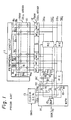
- FIG 1 shows a circuit constitution of the prior art memory device with serial access memory (SAM).
- SAM serial access memory
- reference 10 denotes a RAM cell array having a memory cell M provided at each intersection between a plurality of word lines W1 - W m and a plurality of pairs of bit lines B1 , B1 - B n , B n .
- Reference 11 denotes a peripheral circuit including a decoder arrangement for selecting one of the word lines and one of the pairs of bit lines.
- Reference 12 denotes a SAM cell array having a memory cell MC1 - MC n provided for each of the pairs of bit lines.
- the memory cells MC1 , MC3 , MC5 , ...., MC n-1 corresponding to odd number addresses are connected to a pair of data lines DB0 , DB0 (data bus for odd number addresses) and the memory cells MC2 , MC4 , MC6 , ...., MC n corresponding to even number ones are connected to another pair of data lines DB E , DB E (data bus for even number addresses).
- Each of bit data in the memory cells MC1 - MC n is serially read out.
- Reference 13 denotes a clock generator, which receives a serial access storobe (SAS) signal, divides a frequency of the SAS signal, and generates clocks CK0 and CK E so that, when one of the clocks is at logical high ("H") level, the other is at logical low (“L”) level, and vice versa.
- Reference 14 denotes a multiplexer, which includes N-channel metal oxide semiconductor (NMOS) transistors 16, 17, 18 and 19 connected in series with each of the data lines DB0 , DB0> , DB E and DB E , respectively, and a buffer 15 connected between the transistors 16 - 19 and a serial I/O terminal.
- SAS serial access storobe
- Reference RC denotes a reset circuit, which includes a P-channel MOS (PMOS) transistor 20 connected between the data lines DB0, DB0 (or DB E , DB E ) and PMOS transistor 21, 22 connected in series therebetween.
- PMOS P-channel MOS
- the reset circuit RC When the clock CK0 (or CK E ) is at "L" level, the reset circuit RC short-circuits the data lines DB0 , DB0 (or DB E , DB E ) and brings them to a level of V cc . Namely, the reset circuit RC has a function of bringing the corresponding data bus to a reset state.
- the data in the RAM cell array 10 are read out with a unit of an arbitrary single row, i.e., n bit data, and stored in the SAM cell array 12.
- the stored data are serially read in response to the SAS signal.
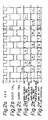
- Figs. 2a to 2f which are timing charts indicating the operation of the device of Fig. 1
- the clocks CK0 and CK E are alternatively raised to "H" level in synchroniza tion with the rise of the SAS signal.
- the clock CK0 is raised to "H” level
- the transistors 16 and 17 in the multiplexer 14 are turned ON and the transistors 20, 21 and 22 in the corresponding reset circuit RC are turned OFF.
- bit data for odd number addresses in the SAM cell array 12 can be read via the data bus DB0 , DB0 and the buffer 15 to the serial I/O terminal.
- the bit data for even number addresses can be read via the data bus DB E , DB E and the buffer 15 to the serial I/O terminal.
- the bit data un the SAM cell array 12 are output alternately and serially to the data buses DB0 , DB0 and DB E , DB E , and read out without interruption to the serial I/O terminal, as shown in Fig. 2f.
- reference t R in Figs. 2d and 2e indicates a reset period in which the corresponding data bus is brought to the reset state.
- bit data "1” to "5" among the n bit data stored in the SAM cell array 12 are allocated to a first transfer data block, and bit data following a bit data "9” are allocated to a second one.
- the last data of the first transfer data block and the head data of the second transfer block coincide with the odd number address.
- the bit data "5" and "9” appear in sequence on the data bus DB0 , DB0 for odd number addresses.
- a reset period t O corresponding to one cycle of the SAS signal is generated between the bit data "5" and "9".
- interruption equal to one cycle of the SAS signal is inevitably generated between the transfer data blocks output from the serial I/O terminal.
- the above interruption would become longer to such an extent that it cannot be disregarded where the number of the blocks is increased. This leads to a lowering in the data transfer speed and thus is not preferable.
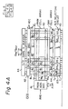
- Figure 4 illustrates a circuit constitution of the semiconductor memory device with a SAM as an embodiment of the present invention. The illustrated constitution is applied to a video RAM device in the form of a chip.
- the device of Fig 4 is constituted by; a RAM cell array 40 having a memory cell M provided at each intersection between a plurality of word lines W1 - W m and a plurality of pairs of bit lines B1 , B 1 - B n , B n ; a random access port portion for effecting an ordinary random access to the RAM cell array; a SAM cell array 44 having a plurality of memory cells MC1 - MC n corresponding to a memory capacity of a single row of the RAM cell array; and a serial access port portion for effecting a serial data access to the SAM cell array.
- the random access port portion includes; a row address decoder 41 which inputs a row address signal ADR in response to a fall of a low active row address strobe signal RAS , selects a word line designated by the row address signal and activates the selected word line; a column address decoder 42 which inputs a column address signal ADC in response to a fall of a low active column address strobe signal CAS , selects a pair of bit lines designated by the column address signal and activates the selected pair of bit lines; and an I/O gate and buffer 43 for effecting the input and output of data (D IN /D OUT ) between the column address decoder 42 and the external in the ordinary random access operation.
- a row address decoder 41 which inputs a row address signal ADR in response to a fall of a low active row address strobe signal RAS , selects a word line designated by the row address signal and activates the selected word line
- a column address decoder 42 which inputs a column address signal A
- the serial access port portion is constituted by a bus selecting circuit 45 having a selecting circuit BS1 - BS n provided for each of the cells in the SAM cell array 44, a multiplexer 46, three pairs of data lines DB0 , DB0 ; DB E , DB E ; DB X , DB X , six reset circuits RC provided at an end and halfway on each pair of data lines, a pointer 57 having a pointer circuit P1 - P n provided for each of the selecting circuits BS1 - BS n , and a control circuit 60.
- a first pair of data lines (data bus) DB0 , DB0 are connected between the multiplexer 46 and the bus selecting circuits BS1 , BS3 , BS5 , Vietnamese, which are connected to the memory cells MC1 , MC3 , MC5 , whereas, corresponding to odd number addresses.
- a second pair of data lines (data bus) DB E , DB E are connected between the multiplexer 46 and the bus selecting circuits BS2 , BS4 , Vietnamese , BS n-1 , which are connected to the memory cells MC2 , MC4 , ...., MC n-1 corresponding to even number addresses.
- a third pair of data lines (data bus) DB X , DB X are connected between the multiplexer 46 and the last bus selecting circuit BS n , which is connected to the memory cell MC n corresponding to the last address.
- the last address corresponds to an odd number address.
- Each of the bus selecting circuits BS1 - BS n includes a pair of NMOS transistors T1 , T2 , which are connected in series with the lines which connect the corresponding memory cell MC1 - MC n to the corresponding data bus.
- the pair of transistors T1 , T2 are turned ON in response to a bus select signal S1 - S n output from the corresponding pointer circuit P1 - P n .
- each of the selecting circuits BS1 - BS n-1 connects the corresponding SAM cell MC1 - MC n-1 to the data bus DB0 , DB0 for odd number addresses or the data bus DB E , DB E for even number addresses, except that the selecting circuit BS n connects the SAM cell MC n to the data bus DB X , DB X for the last address.
- the multiplexer 46 includes NMOS transistors 48, 49, 50, 51, 52 and 53 connected in series with each of the data lines DB0 , DB0 , DB E , DB E , DB X and DB X , respectively, and a buffer 47 connected between the transistors 48 - 53 and a serial I/O terminal.
- the transistors 48 and 49 brings the data bus DB0 and DB0 to a closed or open state in response to a control clock S0 output from the control circuit 60
- the transistors 50 and 51 brings the data bus DB E and DB E to a closed or open state in response to a control clock S E output from the control circuit 60
- the transistors 52 and 53 brings the data bus DB X and DB X to a closed or open state in response to a control clock S X output from the control circuit 60.
- Each of six reset circuits RC includes a PMOS transistor 54 connected between the corresponding pair of data lines and PMOS transistors 55, 56 connected in series therebetween, and short-circuits the corresponding pair of data lines to bring them to the reset state when the control clock S0 , S E or S X from the control circuit 60 is at "L" level.
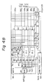
- control circuit 60 Next, a circuit constitution of the control circuit 60 will be described with reference to Fig. 5.
- the control circuit 60 in the present example is constituted by a frequency dividing circuit 61 which responds to the rise of a serial access strobe (SAS) signal and generates a couple of frequency divided signals ACK indicating odd number addresses in the SAM cell array 44, an NMOS transistor 62 which responds to an output signal of an inverter 67 and transmits the frequency divided signal ACK to the multiplexer 46 as the control clock S0 , an NMOS transistor 63 which responds to the bus select signal S n fed from the last pointer circuit P n and pulls the control clock S0 down to "L" level, an inverter 64 which inverts the frequency divided signal ACK to a signal BCK indicating even number addresses in the SAM cell array 44, an NMOS transistor 65 which responds to the output signal of the inverter 67 and transmits the signal BCK to the multiplexer 46 as the control clock S E , an NMOS transistor 66 which responds to the bus select signal S n and pulls the control
- the control circuit 60 outputs the control clock S0 for odd number addresses and the control clock S E for even number addresses alternately and serially in response to the rise of the SAS signal and, when the pointer 57 raises the signal S n indicating the last address in the SAM cell array to "H" level, outputs the third control clock S X replacing the control clocks S0 and S E .
- Each pointer circuit P1 - P n of the pointer 57 substantially has an identical constitution, and is constituted by four PMOS transistors Q1 - Q4 and eight NMOS transistors Q5 - Q12.
- Each source of the transistors Q1 and Q2 is connected to a higher power supply line V cc (5 V), and each drain thereof is connected via transistors Q3, Q5 and Q4, Q6, respectively, to a lower power supply line V ss (0 V).
- Four transistors Q3 - Q6 constitute a flip flop.
- the transistor Q7 (Q8) is connected in parallel to the transistor Q5 (Q6).
- the transistors Q9 and Q11 are connected in series between one of the output nodes of the flip flop and the power supply line V ss , while the transistors Q10 and Q12 are connected in series between another of the output nodes thereof and the line V ss .
- the transistors Q1 and Q7 respond to a corresponding decode signal PC0 - PC n-1 , which is fed from the column address decoder 42.
- the decoder 42 decodes the column address signal ADC in response to the fall of the column address strobe signal CAS and, based on the decoding, selects one bit of n bits. Accordingly, for example, where the column address decoder 42 selects the pair of bit lines B3 , B3 , the corresponding decode signal PC2 is raised to "H" level and the other decode signals PC0 , PC1 and PC3 - PC n-1 are maintained to "L" level.
- the transistors Q2 and Q8 respond to a signal PR of a predetermined level, which is fixed to "L" level in the present example.
- the transistor Q9 of the pointer circuit P i responds to the output signal of the preceding pointer circuit P i-1 , i.e., the bus select signal S i-1 , except that the transistor Q9 of the first pointer circuit P1 responds to a fixed level V ss .
- the transistor Q10 of each pointer circuit P1 - P n responds to signals SL1 - SL n , respectively.
- the signal SL i corresponds to the output signal of the following pointer circuit P i+1 , i.e., the bus select signal S i+1 , except that the signal SL n in the last pointer circuit P n is fixed to "H" level.
- the transistors Q11 of the pointer circuits P1 , P3 , P5 , ., P n for odd number addresses respond to the signal ACK fed from the control circuit 60, and the transistors Q12 thereof respond to the signal BCK fed from the control circuit 60.
- the transistors Q11 of the pointer circuits P2 , P4 , P6 , across, P n-1 for even number addresses respond to the signal BCK, and the transistors Q12 thereof respond to the signal ACK.
- the signal S2 of "H” level is applied to the transistor Q9 in the following pointer circuit P3 , too.
- the signal ACK is raised to "H” level in response to the next rise of the SAS signal (see Fig. 5)
- the transistors Q9 and Q11 in the pointer circuit P3 are brought to the ON state, so that the drain of the transistor Q7 therein is pulled down to “L” level.
- the transistor Q4 in the circuit P3 is turned ON, so that the bus select signal S3 is raised to "H” level.
- the signal ACK is at "H” level. Therefore, when the signal S3 of "H” level is applied to the transistor Q10 in the preceding circuit P2 , the bus select signal S2 is lowered to "L” level.
- the pointer 57 functions as a kind of a preset counter. Namely, in the transfer mode between the RAM and SAM, when the decode signal PC0 - PC n-1 fed from the column address decoder 42 based on the decoding of the column address signal ADC input at the fall of the signal CAS is input to the pointer 57, the bus select signal S1 - S n of the corresponding pointer circuit P1 - P n is preset to "H" level, i.e., "1".
- the pointer 57 When the arbitrary pointer circuit is brought to the preset state in accordance with the timing of the fall of the signal CAS , the pointer 57 counts up the preset value one by one in response to the signal ACK or BCK and outputs each of the select signals S1 - S n in sequence. For example, where the preset value is "1" for the raised circuit P1 , the bus select signal S1 is first raised to "H” level and, then, the signal S2 , S3 , ., S n is raised to "H” level in sequence. When the last select signal S n is output, it is fed to the control circuit 60 and, then, transmitted to the multiplexer 46 as the control clock S X (see Fig. 5).
- bit data "n-4" to "n” among the n bit data stored in the SAM cell array 44 are allocated to a first transfer data block, and that bit data "n-2" to “n” thereamong are allocated to a second one. Therefore, in this case, the column address strobe signal CAS needs to be lowered to "L” level at a timing such that the column address decoder 42 can select the pairs of bit lines B n-4 , B n-4 and B n-2 , B n-2 corresponding to the bit data "n-4" and "n-2".
- the transistors 48 and 49 in the multiplexer 46 are turned ON and the corresponding reset circuits RC cannot function.
- the bit data "n-4" on the data bus DB0 , DB0 is output via the multiplexer 46 to the serial I/O terminal.
- bit data "n-2" and "n-1" are read on the data bus DB0 , DB0 and DB E , DB E , respectively, and serially output to the serial I/O terminal. According, as shown in Fig. 7k, the bit data "n-4" to "n-1" are output to the serial I/O terminal without interruption.
- the last pointer circuit P n When the fifth SAS signal is raised to "H” level, the last pointer circuit P n functions, so that the select signal S n is raised to "H” level. As a result, the transistors T1 and T2 of the last selecting circuit BS n are turned ON, so that the bit data "n” is read on the third data bus DB X , DB X . At the same time, the control circuit 60 pulls the control clocks S0 and S E down to "L” level and output the control clock S X of "H” level.
- the bit data "n” on the data bus DB X , DB X is output to the serial I/O terminal. Therefore, as shown in Fig. 7k, the bit data "n” is output to the I/O terminal without interruption, following the bit data "n-1".
- both of the data buses DB0 , DB0 and DB E , DB E are brought to the level of V cc , i.e., the reset state. Accordingly, when the bit data corresponding to the head address, "n-2" in the present example, of the next transfer data block is transferred the resetting of the data bus DB0 , DB0 corresponding to the bit data "n-2” is already completed. Thus, the head bit data "n-2" of the second data block is output to the serial I/O terminal without interruption, following the last bit data "n” of the first data block.
- the device is provided with the third data bus and constituted such that the information corresponding to the last address of a transfer data block is read on the third data bus and output to the serial I/O terminal. Therefore, when the last bit data is output via the third data bus, it is possible to fully reset he data bus for odd number addresses and the data bus for even number addresses. Thus, irrespective of whether the head bit data of the next data block is for an odd number address or for and even number address, the head bit data can be output to the I/O terminal without interruption, following the last bit data of the first data block. This contributes to the increase in the speed of the serial data transfer between the SAM cell array and the serial I/O terminal.
- the device shown in Fig. 8 is characterized in that the last address of a transfer data block is selectable, although, in the device of Fig. 4 the last address is fixed to "n". Since the circuit constitution of Fig. 8 and the operation thereof are the same as those of Fig. 4 in most parts, only the differences between them are hereinafter referred to.
- the third data bus DB X , DB X is connected between the multiplexer 46 and all of the bus selecting circuits BS1′ - BS n ′.
- the control circuit 60′ outputs the control clock S X in response to an external control signal TR / OE , although, in the embodiment of Fig. 4, the control clock S X is determined by the bus select signal S n from the pointer 57.
- the control signal TR / OE is raised to "H" level at a timing such that the column address decoder can select a pair of bit lines corresponding to the last address of a transfer data block. Accordingly, the control circuit 60′ has a function of detecting the last address of the transfer data block based on the logical level of the control signal TR / OE .
- Reference 58 denotes a counter having a counter circuit C1- C n provided for each of the selecting circuits BS1′ - BS n ′.
- the counter 58 responds to the SAS signal and the control signal TR / OE , raises one of bus change signals S1′ - S n ′ to "H" level, and supplies the "H" level signal to the corresponding bus selecting circuit BS1′ -BS n ′.
- the control circuit 60′ detects that the last address of the transfer data block is "5".
- the counter 58 raises only the fifth bus change signal S5′ to "H” level and transmits it to the corresponding bus selecting circuit BS5′.
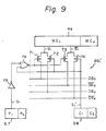
- a circuit constitution of the bus selecting circuit 45′ shown in Fig. 8 will be described with reference to Fig. 9.
- the illustration of Fig. 9 representatively shows the constitution of the selecting circuit BS1′.
- the bus selecting circuit BS1′ illustrated in Fig. 9 is constituted by an NMOS transistor 71 which responds to an output signal of an NOR gate 76 and connects the bit line B1 of the corresponding SAM cell MC, to the data line DB0 , an NMOS transistor 72 which responds to the bus change signal S1′ from the corre sponding counter circuit C1 and connects the bit line B1 to the data line DB X , an NMOS transistor 73 which responds to the output signal of the NOR gate 76 and connects the complementary bit line B1 to the complementary date line DB0 , an NMOS transistor 74 which responds to the bus change signal S1′ and connects the bit line B1 to the complementary data line DB X , an inverter 75 responding to the bus select signal S1 from the corresponding pointer circuit P1 , and the NOR gate 76 responding to the output signal of the inverter 75 and the bus change signal S1′.
- Figures 10a to 10n are timing charts indicating the operation of the device of Fig. 8.
- bit data "1" to "5" among the n bit data stored in the SAM cell array 44 are allocated to the first transfer data block, and that bit data "9” to "11” thereamong are allocated to the second one.
- the read and output of the head bit data of the transfer data block are determined by the timing of the fall of the signal CAS , and those of the last bit data thereof are determined by the timing of the rise of the external control signal TR / OE . Since the forms of generation of the other signals are easily deduced from those in the embodiment of Fig. 4, the explanation thereof will be omitted.
- the device is constituted such that the bit data corresponding to the last address of the transfer data block is read on the third data bus DB X , DB X and output via the multiplexer 46 to the serial I/O terminal. Therefore, during the serial data transfer, both of the data buses DB0 , DB0 and DB E , DB E can be fully reset. As a result, the head bit data "9" of the second data block can be output to the I/O terminal without interruption, following the last bit data "5" of the first data block, as shown in Fig. 10n.
- the bit data corresponding to the last address of the transfer data block is read on the third data bus DB X , DB X , it is not restrictive.
- the third data bus may transfer the bit data corresponding to the head address of the transfer data block.
- the control circuit 60 outputs the control clock S X in response to the bus select signal S1 from the pointer 57.
- the important feature is that the device is constituted such that bit data of either of the head address or the last address between the transfer data blocks in sequence is read on the third data bus DB X , DB X .
- the SAM cell array, the bus selecting circuit and the pointer may be constituted in a duplicated form.
- a multiplexer 59 is newly provided.
- the multiplexer 59 switches one of the SAM cell arrays 44a and 44b to the RAM cell array 40 in the transfer mode between the RAM and SAM.
- the SAM cell array 44a (44b) is associated with the bus selecting circuit 45a (45b) and the pointer 57a (57b).
- the second SAM cell array 44b can be associated with the RAM cell array 40 via the multiplexer 59, and vice versa. Namely, when one of the SAM cell arrays participates in the serial data transfer, the other thereof can receive bit data from the RAM cell array and be prepared for the next participation in the data transfer. Thus, this contributes to a further increase in the speed of the serial data transfer.
Landscapes
- Engineering & Computer Science (AREA)
- Microelectronics & Electronic Packaging (AREA)
- Computer Hardware Design (AREA)
- Multimedia (AREA)
- Databases & Information Systems (AREA)
- Dram (AREA)
Applications Claiming Priority (2)
| Application Number | Priority Date | Filing Date | Title |
|---|---|---|---|
| JP62307936A JPH0748301B2 (ja) | 1987-12-04 | 1987-12-04 | 半導体記憶装置 |
| JP307936/87 | 1987-12-04 |
Publications (3)
| Publication Number | Publication Date |
|---|---|
| EP0319432A2 true EP0319432A2 (de) | 1989-06-07 |
| EP0319432A3 EP0319432A3 (en) | 1990-11-28 |
| EP0319432B1 EP0319432B1 (de) | 1993-09-08 |
Family
ID=17974956
Family Applications (1)
| Application Number | Title | Priority Date | Filing Date |
|---|---|---|---|
| EP88403061A Expired - Lifetime EP0319432B1 (de) | 1987-12-04 | 1988-12-02 | Halbleiterspeicheranordnung mit einem seriellen Zugriffsspeicher |
Country Status (5)
| Country | Link |
|---|---|
| US (1) | US4930108A (de) |
| EP (1) | EP0319432B1 (de) |
| JP (1) | JPH0748301B2 (de) |
| KR (1) | KR930004669B1 (de) |
| DE (1) | DE3883935T2 (de) |
Cited By (1)
| Publication number | Priority date | Publication date | Assignee | Title |
|---|---|---|---|---|
| EP0563656A3 (de) * | 1992-03-30 | 1994-01-12 | Toshiba Kk |
Families Citing this family (12)
| Publication number | Priority date | Publication date | Assignee | Title |
|---|---|---|---|---|
| JP2880547B2 (ja) * | 1990-01-19 | 1999-04-12 | 三菱電機株式会社 | 半導体記憶装置 |
| JPH0821233B2 (ja) * | 1990-03-13 | 1996-03-04 | 株式会社東芝 | 画像メモリおよび画像メモリからデータを読み出す方法 |
| JP2928654B2 (ja) * | 1991-04-10 | 1999-08-03 | 株式会社東芝 | マルチポートdram |
| US5206821A (en) * | 1991-07-01 | 1993-04-27 | Harris Corporation | Decimation circuit employing multiple memory data shifting section and multiple arithmetic logic unit section |
| JPH05101646A (ja) * | 1991-10-07 | 1993-04-23 | Mitsubishi Electric Corp | デユアルポートメモリ |
| DE69322054T2 (de) * | 1992-10-16 | 1999-04-01 | Matsushita Electric Industrial Co., Ltd., Kadoma, Osaka | Gerät zur Aufzeichnung von Datensignalen mittels Steuerung der Frequenzcharakteristiken der Datensignale |
| KR0141665B1 (ko) * | 1994-03-31 | 1998-07-15 | 김광호 | 비디오램 및 시리얼데이타 출력방법 |
| US6167486A (en) * | 1996-11-18 | 2000-12-26 | Nec Electronics, Inc. | Parallel access virtual channel memory system with cacheable channels |
| US6708254B2 (en) | 1999-11-10 | 2004-03-16 | Nec Electronics America, Inc. | Parallel access virtual channel memory system |
| US6509851B1 (en) * | 2000-03-30 | 2003-01-21 | Cypress Semiconductor Corp. | Method for using a recovered data-encoded clock to convert high-frequency serial data to lower frequency parallel data |
| JP4857544B2 (ja) * | 2004-10-29 | 2012-01-18 | 富士電機株式会社 | 可撓性基板の穴あけ加工方法、薄膜基板の貫通孔加工装置、および薄膜太陽電池の製造装置 |
| US8208314B2 (en) | 2010-06-01 | 2012-06-26 | Aptina Imaging Corporation | Sequential access memory elements |
Family Cites Families (5)
| Publication number | Priority date | Publication date | Assignee | Title |
|---|---|---|---|---|
| JPS6072020A (ja) * | 1983-09-29 | 1985-04-24 | Nec Corp | デュアルポ−トメモリ回路 |
| JPS60140924A (ja) * | 1983-12-27 | 1985-07-25 | Nec Corp | 半導体回路 |
| DE3586523T2 (de) * | 1984-10-17 | 1993-01-07 | Fujitsu Ltd | Halbleiterspeicheranordnung mit einer seriellen dateneingangs- und ausgangsschaltung. |
| CA1293565C (en) * | 1986-04-28 | 1991-12-24 | Norio Ebihara | Semiconductor memory |
| JPS62287497A (ja) * | 1986-06-06 | 1987-12-14 | Fujitsu Ltd | 半導体記憶装置 |
-
1987
- 1987-12-04 JP JP62307936A patent/JPH0748301B2/ja not_active Expired - Lifetime
-
1988
- 1988-12-01 US US07/278,502 patent/US4930108A/en not_active Expired - Fee Related
- 1988-12-02 EP EP88403061A patent/EP0319432B1/de not_active Expired - Lifetime
- 1988-12-02 DE DE88403061T patent/DE3883935T2/de not_active Expired - Fee Related
- 1988-12-03 KR KR1019880016134A patent/KR930004669B1/ko not_active Expired - Fee Related
Cited By (2)
| Publication number | Priority date | Publication date | Assignee | Title |
|---|---|---|---|---|
| EP0563656A3 (de) * | 1992-03-30 | 1994-01-12 | Toshiba Kk | |
| US5343425A (en) * | 1992-03-30 | 1994-08-30 | Kabushiki Kaisha Toshiba | Semiconductor video memory having multi-ports |
Also Published As
| Publication number | Publication date |
|---|---|
| EP0319432B1 (de) | 1993-09-08 |
| KR930004669B1 (ko) | 1993-06-02 |
| US4930108A (en) | 1990-05-29 |
| KR890010914A (ko) | 1989-08-11 |
| EP0319432A3 (en) | 1990-11-28 |
| JPH0748301B2 (ja) | 1995-05-24 |
| JPH01149298A (ja) | 1989-06-12 |
| DE3883935D1 (de) | 1993-10-14 |
| DE3883935T2 (de) | 1994-01-05 |
Similar Documents
| Publication | Publication Date | Title |
|---|---|---|
| US4511965A (en) | Video ram accessing system | |
| US6928028B2 (en) | Synchronous dynamic random access memory for burst read/write operations | |
| US4876670A (en) | Variable delay circuit for delaying input data | |
| EP0319432B1 (de) | Halbleiterspeicheranordnung mit einem seriellen Zugriffsspeicher | |
| KR940000148B1 (ko) | 듀얼포트 반도체 기억장치 | |
| US6078546A (en) | Synchronous semiconductor memory device with double data rate scheme | |
| US5860084A (en) | Method for reading data in a memory cell | |
| JP3317187B2 (ja) | 半導体記憶装置 | |
| US5892730A (en) | Synchronous semiconductor memory device operable in a plurality of data write operation modes | |
| US4899310A (en) | Semiconductor memory device having a register | |
| US4858190A (en) | Dual port semiconductor memory having random and serial access modes | |
| KR100292552B1 (ko) | 데이타 전송방법 및 반도체 메모리 | |
| EP0136414A2 (de) | Dynamischer Speicher mit schnellem seriellem Modus | |
| US4961169A (en) | Method of and apparatus for generating variable time delay | |
| US20010003429A1 (en) | Logical circuit | |
| EP0388175B1 (de) | Halbleiter-Speichereinrichtung | |
| US4870621A (en) | Dual port memory device with improved serial access scheme | |
| EP0260578A2 (de) | Speicheranordnung mit zwei multiplexierten E/A-Leitungspaaren | |
| US4766570A (en) | Semiconductor memory device | |
| US4951251A (en) | Semiconductor memory device | |
| US5523981A (en) | Semiconductor memory device | |
| US5206832A (en) | Semiconductor memory device | |
| US5325332A (en) | Dual port semiconductor memory device | |
| US5280448A (en) | Dynamic memory with group bit lines and associated bit line group selector | |
| US4485461A (en) | Memory circuit |
Legal Events
| Date | Code | Title | Description |
|---|---|---|---|
| PUAI | Public reference made under article 153(3) epc to a published international application that has entered the european phase |
Free format text: ORIGINAL CODE: 0009012 |
|
| AK | Designated contracting states |
Kind code of ref document: A2 Designated state(s): DE FR GB |
|
| PUAL | Search report despatched |
Free format text: ORIGINAL CODE: 0009013 |
|
| AK | Designated contracting states |
Kind code of ref document: A3 Designated state(s): DE FR GB |
|
| 17P | Request for examination filed |
Effective date: 19901224 |
|
| 17Q | First examination report despatched |
Effective date: 19921027 |
|
| GRAA | (expected) grant |
Free format text: ORIGINAL CODE: 0009210 |
|
| AK | Designated contracting states |
Kind code of ref document: B1 Designated state(s): DE FR GB |
|
| REF | Corresponds to: |
Ref document number: 3883935 Country of ref document: DE Date of ref document: 19931014 |
|
| ET | Fr: translation filed | ||
| PLBE | No opposition filed within time limit |
Free format text: ORIGINAL CODE: 0009261 |
|
| STAA | Information on the status of an ep patent application or granted ep patent |
Free format text: STATUS: NO OPPOSITION FILED WITHIN TIME LIMIT |
|
| 26N | No opposition filed | ||
| PGFP | Annual fee paid to national office [announced via postgrant information from national office to epo] |
Ref country code: GB Payment date: 19951123 Year of fee payment: 8 |
|
| PGFP | Annual fee paid to national office [announced via postgrant information from national office to epo] |
Ref country code: FR Payment date: 19951212 Year of fee payment: 8 |
|
| PGFP | Annual fee paid to national office [announced via postgrant information from national office to epo] |
Ref country code: DE Payment date: 19951214 Year of fee payment: 8 |
|
| PG25 | Lapsed in a contracting state [announced via postgrant information from national office to epo] |
Ref country code: GB Effective date: 19961202 |
|
| GBPC | Gb: european patent ceased through non-payment of renewal fee |
Effective date: 19961202 |
|
| PG25 | Lapsed in a contracting state [announced via postgrant information from national office to epo] |
Ref country code: FR Effective date: 19970829 |
|
| PG25 | Lapsed in a contracting state [announced via postgrant information from national office to epo] |
Ref country code: DE Effective date: 19970902 |
|
| REG | Reference to a national code |
Ref country code: FR Ref legal event code: ST |